Article

Double-Layer Microstrip Band Stop Filters Etching Periodic Ring Electromagnetic Band Gap Structures

1
College of Information and Communication Engineering, Harbin Engineering University, Harbin 150001 China
2
School of Electrical Engineering, Northeast Electric Power University, Jilin 132012, China
3
Science and Technology on Complex System Control and Intelligent Agent Cooperation Laboratory, Beijing 100074, China
*
Author to whom correspondence should be addressed.
Electronics 2020, 9(8), 1216; https://doi.org/10.3390/electronics9081216
Submission received: 31 March 2020 / Revised: 9 July 2020 / Accepted: 17 July 2020 / Published: 28 July 2020

Abstract

:
The electromagnetic band gap structure (EBGs) is widely used in microwave engineering, such as amplifiers, waveguides, microstrip filters, due to the fact of its excellent band stop characteristics. In this paper, three kinds of microstrip band stop filters were proposed which were etched with a hexagonal ring EBGs, octagonal ring EBGs and elliptical ring EBGs. Firstly, the etching coefficient of a band stop filter is proposed, and the performance of filters with different etching coefficient was analyzed. Secondly, the equivalent circuit of an EBGs band stop filter is proposed. By comparing the simulation results using advanced design system (ADS) and high frequency structure simulator (HFSS), it was found that the simulation results had the same −10 dB stopband width which verifies the correctness of the equivalent circuit model. Finally, three kinds of microstrip stopband filters were fabricated and measured. The experimental results of the −10 dB stopband width and resonant frequency were in good agreement with the simulation results. The −10 dB stopband fractional bandwidth of the three kinds of microstrip stopband filters was more than 63%. The proposed microstrip band stop filters can be widely used in microwave devices with a wide stopband.

1. Introduction

The photonic band gap (PBG) structure has a certain periodic structure which can prevent the propagation of microwave in a certain frequency range [1]. The electromagnetic band gap structure (EBGs) originates from the PBG structure which has the characteristics of band resistance and slow wave [2]. In recent years, EBGs has been widely used in microwave device design. In the application of microwave power amplifiers, it has usually been used to improve the efficiency and output power of power amplifiers. In the design of microstrip antennas, it is mainly used to improve the performance of the antenna [3]. In the application of microstrip filters, its superior broad stopband characteristic is suitable for microwave band stop filters [4,5,6,7,8,9].
Microstrip filters based on a variety of EBG structures are realized by a few techniques, and they mainly include the following categories. The first is to realize the filter with notch by coupling an EBGs, adjusting the coupling distance and the size of the unit EBGs. In Reference [4], a microstrip filter based on the Archimedes spiral EBGs is proposed. In Reference [5], a microstrip filter is realized via a coupling T-shaped resonator, and an asymmetric coupling line band-pass filter is proposed in Reference [6], and the performance of the filter is adjusted by adding coupling variables. In Reference [7], an ultra-wideband bandpass filter based on a coupled EBGs is proposed. The second is based on the periodic EBGs which reduces the passband ripple, increases the stopband width, and achieves better band stop characteristics. For example, Reference [8] proposed a DP–EBG structure to achieve band stop characteristics; Reference [9] proposed a filter embedded in a multi-mode resonator; Reference [10] proposed a filter based on a tapered Cauchy microstrip Koch fractal EBGs; and Reference [11] proposed a filter based on a multi-cycle conical etching EBGs. The third is based on the integration of EBGs and a multi-layer PCB. For example, multi-layer PCB adopts the locally embedded planar EBGs [12] and biplane EBG microstrip filter [13]. The fourth is to optimize the EBGs based on high performance optimization algorithm, and analyze its band resistance characteristics to obtain better band resistance. In Reference [14], Particle swarm optimization (PSO) is used to optimize EBGs, and in Reference [15] PSO is used to optimize the EBG common mode filter by using an artificial neural network.
In this paper, three kinds of double-layer microstrip stopband filters with an etched EBG ring structure are proposed. First, a band stop filter based on a gradient line is proposed. In the upper layer of the dielectric plate, the basic band stop filter was realized by using the butterfly gradient microstrip line. The periodic elliptical ring, hexagonal ring, and octagonal ring were etched on the floor, further increasing the stopband width of −10 dB and the maximum attenuation. Second, the influence of the etching factor of the three band stop filters on the band stop width and attenuation was analyzed, and the equivalent circuit of the band top filter was further analyzed. The correctness of the proposed equivalent circuit model was verified by comparing the simulation and measured results. Finally, the three band stop filters were compared with those proposed in other studies. The proposed filters etched with three kinds of EBGs rings can be applied to the broadband band stop RF devices.

2. Design of Microstrip Band Stop Filter

2.1. Design Principle of Microstrip Band Stop Filter

The three band stop filters designed in this paper were composed of a two-layer EBGs. The top layer was the patch microstrip line of butterfly element, and the bottom layer was etched with three different periodic ring EBGs on the floor. According to Reference [14], when the period of the butterfly element is six, the band stop filter can obtain good stopband characteristics and small passband ripple. The dielectric material was Rogers ro4003, the thickness of the dielectric plate was 1.5 mm, and the relative dielectric constant was 3.55. According to Bragg reflection conditions, Formulas (1)–(4) can be derived. The distance between two adjacent circles on the ground plate was d1, β was the phase constant of the dielectric plate, λg was the wavelength of the waveguide, f0 was the center frequency of the band resistance, εeff was the effective dielectric constant plate of the medium, and C was the speed of light. The central frequency of the three filters was 5.2 GHz, the period d1 and d2 of the upper butterfly structure were 17.1 mm, and the corresponding w1 was 3.5 mm and w2 was 0.2 mm.
β × d 1 = π
β = 2 π λ g
λ g = C f 0 × ε e f f
d 1 = λ g 2
The top layer of the three double-layer band stop filters proposed in this paper adopted the butterfly gradient structure with a thickness of 0.035 mm. The top view and the 3D view are shown in Figure 1a,b, respectively. In order to analyze the effect of w1 and w2 on the band stop, HFSS was adopted to sweep the frequency from 2 GHz to 8 GHz for w1 and w2.
As shown in Figure 2a, with the increase of w1, the −10 dB bandwidth increased from 1.59 GHz to 1.91 GHz, the maximum stopband attenuation increased from 19.41 dB to 23.95 dB, the low-frequency ripple decreased from 2.73 dB to 2.29 dB, and the high-frequency ripple increased from 1.99 dB to 3.93 dB. As shown in Figure 2b, with the increase of w2, the −10 dB bandwidth decreased from 2.01 GHz to 1.49 GHz, the maximum stopband attenuation decreased from 25.39 dB to 18.3 dB, and the low-frequency ripple and high-frequency ripple decreased accordingly.
As shown in Figure 3a, with the increase of d1, the resonance frequency decreased continuously, but the −10 dB bandwidth and the maximum stopband attenuation increased. The simulation of the band stop filter based on the asymptote structure are shown in Figure 3b. The frequency of stopband resonance center was set at 5.2 GHz, and the size of gradient line optimized by HFSS sweeping was as follows: d1 = d2 = 17.1 mm; w = 10 mm; w1 = 3.5 mm; w2 = 0.2 mm; dielectric constant = 3.55; and thickness = 1.5 mm.

2.2. Band Stop Filter with Etched Periodic Hexagon Ring EBG Structure

The upper layer of the microstrip band stop filter is a butterfly-shaped gradient line which is made of copper with a thickness of 0.034 mm. The floor of the filter is covered with copper and etched with a hexagon ring EBGs. The etched depth is equal to the thickness of copper, which is 0.034 mm. The side length of the outer hexagon is c1, and the side length of the inner hexagon is c2. The etching factor of hexagon is kh = c2/c1. A perspective view of a microstrip band stop filter etched with a periodic hexagon ring on the floor is shown in Figure 4a, and Figure 4b is a 3D view of a microstrip band stop filter etched with a periodic hexagon ring modeled using HFSS.

2.3. Band Stop Filter of Etched Periodic Octagonal Ring EBG Structure

The upper layer of the microstrip band stop filter is a butterfly-shaped gradient line which is made of copper with a thickness of 0.034 mm. The floor of the filter is covered with copper and etched with an octagonal ring EBGs. The etched depth is equal to the thickness of copper which is 0.034 mm. Figure 5a shows a perspective view of a microstrip band stop filter etched with a periodic octagon ring on the floor. The center distance of the outer octagon is e1, the center distance of the inner octagon is e2, and the relationship between ko = e2/e1. Figure 5b is a 3D diagram of a microstrip band stop filter with periodic octagonal ring etched by HFSS.

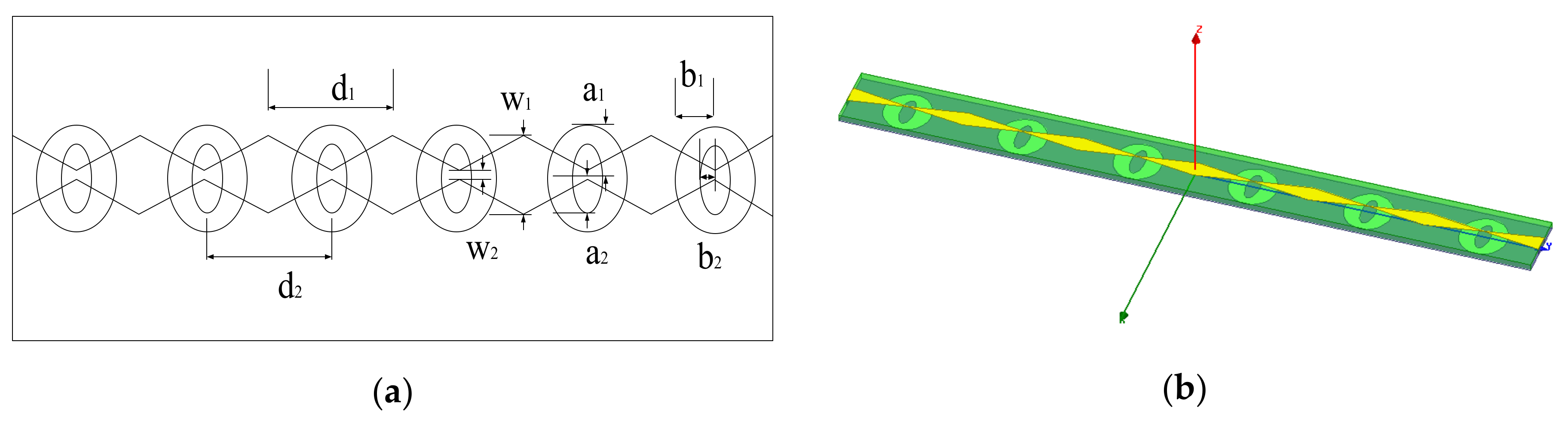
2.4. Band Stop Filter of Etched Periodic Elliptic Ring EBG Structure

The upper layer of the microstrip band stop filter is a butterfly-shaped gradient line which is made of copper with thickness of 0.034 mm. The floor of the filter is covered with copper and etched with an elliptical ring EBGs. The major axis of the outer ellipse ring is a1, the minor axis is b1, the major axis of the inner ellipse ring is a2, and the minor axis is b2. The ratio of the long axis to the short axis of the outer elliptic ring is ra1, ra1 = b1/a1. The ratio of the major axis to the minor axis is ra2, ra2 = b2/a2. The proportion of the long axis and the short axis of the inner and outer elliptic rings is equal, that is ra = ra1 = ra2. Let the etching factor of elliptical ring be ke, ke = a2/a1. Figure 6a is a perspective view of a microstrip band stop filter etched with a periodic elliptical ring, and Figure 6b is a 3D view of a microstrip band stop filter etched with a periodic elliptical ring modeled with HFSS.

3. Discussions and Results

3.1. Analysis of Band Stop Filter with an Etched Periodic Hexagon Ring EBG Structure

In order to analyze the influence of the etching coefficient of a band stop filter with a hexagon ring, we used HFSS to analyze the frequency sweep of kh, c1 = 3.6 mm, where the kh value was 0.5~0.9, and the step size was 0.1. The center frequency was 5.2 GHz, and the optimized parameters were c1 = 4.2 mm and kh = 0.22. As shown in Figure 7a,b, when c1 = 3.6 mm, as kh increased from 0.5 to 0.9, the maximum attenuation of the stopband decreased from 41.9 dB to 36 dB, the bandwidth of −10 dB decreased from 3.05 GHz to 2.66 GHz, and the resonance frequency of band stop filter decreased from 5.24 GHz to 5.2 GHz.
As shown in Figure 8a, when kh = 0.3 and c1 increased from 3.0 mm to 3.8 mm, the maximum attenuation of band resistance increased from 35.56 dB to 42.87 dB, and the −10 dB bandwidth increased from 2.66 GHz to 3.07 GHz, but the ripple of high and low frequency increased slightly. As shown in Figure 8b, the simulation results of the single-layer graded linear EBGs band stop filter, the filter in Reference [14] and the proposed double-layer band stop filter etching hexagon ring EBGs were compared. The results showed that the performance of the double-layer band-stop filter was obviously better than the former two. When the resonant frequency was 5.2 GHz, c1 = 4.2 mm, kh = 0.22, the −10 dB band stop width was 3.34 GHz and the maximum band resistance attenuation was 48.84 dB.
Pictures of the top layer and bottom layer of the microstrip band stop filter based on the gradient line structure and etched hexagon ring EBGs are shown in Figure 9a. The comparison between the measured and the simulation is shown in Figure 9b. The results showed that the resonance frequency of the band stop filter was 5.2 GHz, the stopband width of −10 dB was 3.29 GHz, and the maximum attenuation of the stopband was 44.83 dB. The experimental results of the −10 dB stopband width and resonant frequency were in good agreement with the simulation results. The physical test photos and the physical measurement results of the band stop filter etched periodic hexagon ring EBGs are shown in Figure 10a,b. The performance of the band stop filter was tested with the S5180 vector network analyzer by Copper Mountain Technologies. The vector network analyzer was directly connected to the amplitude and phase stabilization test module of N small a type (N-SMA) using the Gore test cable. The calibration was carried out at the SMA port of the test cable of the vector net, and the reference end face was automatically moved to the calibration end face after calibration.
Taking the microstrip band stop filter with etched periodic hexagon ring as an example, the equivalent circuit of band stop filter was analyzed. The equivalent lumped circuit of the microstrip band stop filter based on gradient line EBGs is shown in Figure 11a. The equivalent lumped circuit of the microstrip band stop filter etched with periodic hexagon ring is shown in Figure 11b. The ring EBGs is etched on the floor of the microstrip band stop filter of the asymptote, which is equivalent to adding inductance capacitance (LC) series resonance in the asymptote equivalent circuit and improving the stopband width of the circuit. The three resonant frequencies of the stopband are determined by inductance capacitance series resonance as shown in Formula (5).
f i = 1 2 π L i C i i = 1 , 2 , 3
Advanced design system (ADS) is used to simulate the equivalent lumped circuit of the microstrip band stop filter etched with periodic hexagon ring. The LC parameters are optimized as shown in Table 1. As shown in Figure 12, the simulation results of ads and HFSS show that they have the same −10 dB stopband width, which verifies the correctness of the proposed equivalent circuit.

3.2. Analysis of Band Stop Filter of Etched Periodic Octagonal Ring EBG Structure

In order to analyze the influence of etching coefficient ko on the performance of the octagonal band stop filter, the scanning frequency of ko was analyzed using HFSS, and the sweep range of ko was from 0.5 to 0.9 in steps 0.1 with the condition e1 = 3.6 mm. The optimized parameters of HFSS were e1 = 4.1 mm and ko = 0.25. As shown in Figure 13a,b, when e1 = 3.6 mm, the maximum attenuation of band stop decreased from 43.1 dB to 36.3 dB, as ko increased from 0.5 to 0.9, the bandwidth of −10 dB decreased from 3.1 GHz to 2.67 GHz, and the resonance frequency of the band stop filter decreased from 5.24 GHz to 5.2 GHz.
As shown in Figure 14a, when ko = 0.3 and e1 increased from 3.0 mm to 3.8 mm, the maximum attenuation of the band stop increased from 38.1 dB to 44.41 dB, and the −10 dB bandwidth increased from 2.74 GHz to 3.13 GHz, but the high and low frequency ripple slightly increased. As shown in Figure 14b, the HFSS simulation results of single-layer gradual linear EBGs band stop filter, the filter proposed in Reference [14], and the double-layer band stop filter etching octagonal ring EBGs were compared. The results showed that the performance of the double-layer band stop filter was better than the former two filters. When the resonance frequency was 5.2 GHz and e1 = 4.1 mm, ko = 0.25, the band stop width of −10 dB was 3.46 GHz, and the maximum band stop attenuation was 50.25 dB. The simulation results showed that by increasing e1 or decreasing the etching factor ko, the band stop width of the filter can be increased and the band stop attenuation can be increased.
The pictures of the top layer and bottom layer of the microstrip band stop filter based on the gradient line structure and etched octagonal ring EBGs with SMA joint are shown in Figure 15a. The comparison between the measured and the simulation is shown in Figure 15b. The performance of the band stop filter was tested with the S5180 vector network analyzer by Copper Mountain Technologies.
The results showed that the resonance frequency of the band stop filter was 5.2 GHz, the stopband width of −10 dB was 3.41 GHz, and the maximum attenuation of the stopband was 49.24 dB. The experimental results of the −10 dB stopband width and resonant frequency were in good agreement with the simulation results. The physical test photos and the physical measurement results of the band stop filter etched periodic hexagon ring EBGs are shown in Figure 16a,b.

3.3. Analysis of Band Stop Filter with Etched Periodic Elliptic Ring EBG Structure

In order to analyze the influence of etching coefficient ke on the performance of band stop filter etched elliptical ring EBGs. In the case of ra = ra1 = ra2, the frequency sweep of ke was analyzed using HFSS. The relationship between etching coefficient and −10 dB band stop bandwidth, maximum insertion loss, and passband ripple were analyzed.
When the resonance frequency was 5.2 GHz, the optimized parameters were a1 = 4.1 mm, ra = 0.95, and ke = 0.24. As shown in Figure 17a,b, a1 = 3.6 mm, ra = ra1 = ra2 = 0.85, when ke increased from 0.5 to 0.9, the maximum attenuation of band stop decreased from 42.6 dB to 36.9 dB, the bandwidth of −10 dB decreased from 3.04 GHz to 2.72 GHz, and the resonance frequency of the band stop filter decreased from 5.22 GHz to 5.2 GHz.
As shown in Figure 18a, as ra increased from 0.5 to 0.9, the maximum attenuation of the band stop increased from 37.29 dB to 43.25 dB, −10 dB bandwidth increased from 3.77 GHz to 3.69 GHz, low-frequency ripple increased from 3.8 dB to 6.17 dB, and high-frequency ripple increased from 4.46 dB to 9.75 dB.
As shown in Figure 18b, the microstrip band stop filter based on single-layer gradient EBGs, the band stop filter proposed in Reference [14], and the double-layer band stop filter etched with tthe elliptical ring EBGs were compared. The results showed that the band stop filter etched with elliptical ring EBGs increased the −10 dB stopband width and the maximum attenuation of stopband, but the ripple in the band also increased.
The top layer and bottom layer of the microstrip band stop filter based on the gradient line structure and etched elliptical ring EBGs with SMA joint are shown in Figure 19a. The comparison between the measured and the simulation is shown in Figure 19b. The performance of the band stop filter was tested with the S5180 vector network analyzer by Copper Mountain Technologies. The results showed that the resonance frequency of the band stop filter was 5.2 GHz, the stopband width of −10 dB was 3.46 GHz, and the maximum attenuation of the stopband was 48.57 dB. The experimental results of the −10 dB stopband width and resonant frequency were in good agreement with the simulation results. The physical test photos and the physical measurement results of the band stop filter etched periodic elliptical ring EBGs are shown in Figure 20a,b.
In order to compare the effect of three etching factors on the stopband characteristics of the three band stop filters, under the condition of a1 = c1 = e1 = 3.6 mm, Figure 21a compares the −10 dB bandwidth with the three etching factors, and Figure 21b analyzes the maximum stopband attenuation with the three etching factors. Simulation results show that the curves of the −10 dB bandwidth of stopband and the maximum attenuation of ke are in good agreement with the curves of kh which shows that the etching factor ke and kh can achieve the same stopband characteristics. Therefore, when a1 = c1 is determined, the required −10 dB bandwidth and the maximum attenuation of the stopband can be adjusted by changing ke or kh.
In this paper, three kinds of double-layer microstrip band stop filters were proposed which were designed with a butterfly-shaped gradual microstrip line on the upper layer of the dielectric plate and the EBGs of a periodic elliptic ring, hexagonal ring, and octagonal ring etched on the floor.

4. Conclusions

By etching the EBGs, a wider band stop and a larger band stop attenuation microstrip band stop filter were realized comparing Reference [14]. Given that a1, c1, and e1 were constant, the −10 dB bandwidth and the maximum attenuation of the three microstrip stop band filters decreased with the increase of the etching parameters ke, kh, and ko. The simulation of the designed filter and other band stop filters are compared in Table 2. Compared with References [14] and [15], the stopband center frequency of 5.2 GHz, the −10 dB fractional bandwidths of the three stopband filters proposed in this paper were all greater than 63% which is significantly larger than the former two.
In this paper, three kinds of double-layer microstrip band stop filters were proposed. The same butterfly gradient microstrip line was used in the upper layer of the dielectric plate, and the periodic elliptical ring, hexagonal ring, and octagonal ring were etched on the floor. Compared with References [14] and [15], the three band stop filters designed in this paper had wider stopband widths and larger maximum attenuations.
In the case of c1 = e1 and kh = ko, the trend of maximum attenuation and relative bandwidth of the band stop filter etched with elliptical ring EBGs and the band stop filter etched with hexagon ring EBGs were consistent.
The simulation and measurement results show that the maximum attenuation and the stopband width of −10 dB can be improved by reducing the corrosion factor of the three microstrip band stop filters. The fractional stopband bandwidths of the three microstrip band stop filters were all over 63%, which can be used in radio frequency (RF) devices with wide stopband bandwidth requirements. In practical application, on the basis of ensuring performance, the filter size should be further reduced and the cost should be reduced.

Author Contributions

Conceptualization, methodology, software, validation, formal analysis, investigation, resources, collection and drawing of simulation data and writing—original draft preparation, X.Z.; Writing—review and editing, visualization, supervision, T.J.; Physical testing and testing report, H.L.; Project administration, funding acquisition, Y.W. All authors have read and agreed to the published version of the manuscript.

Funding

This paper was funded by the National Natural Science Foundation of China (61803356), the International Exchange Program of Harbin Engineering University for Innovation-Oriented Talents Cultivation. This work was partially supported by the National Key Research and Development Program of China (2016YFE0111100), Key Research and Development Program of Heilongjiang (GX17A016), the Science and Technology Innovative Talents Foundation of Harbin (2016RAXXJ044), the Natural Science Foundation of Beijing (4182077), and China Postdoctoral Science Foundation (2017M620918).

Acknowledgments

This paper was funded by the International Exchange Program of Harbin Engineering University for Innovation-Oriented Talents Cultivation. This paper was funded by the National Natural Science Foundation of China (61803356).

Conflicts of Interest

The authors declare no conflict of interest. The founding sponsors had no role in the design of the study; in the collection, analyses, or interpretation of data; in the writing of the manuscript, and in the decision to publish the results.

References

  1. Balakin, A.V.; Bushuev, V.A.; Mantsyzov, B.I.; Ozheredov, I.A.; Petrov, E.V.; Shkurinov, A.P.; Masselin, P.; Mouret, G. Enhancement of sum frequency generation near the photonic band gap edge under the quasiphase matching conditions. Phys. Rev. E 2001, 63, 046609. [Google Scholar] [CrossRef] [PubMed] [Green Version]
  2. Kim, M. A Compact EBG Structure with Wideband Power/Ground Noise Suppression Using Meander-Perforated Plane. IEEE Trans. Electromagn. Compat. 2015, 57, 595–598. [Google Scholar] [CrossRef]
  3. Hassan, M.A.M.; Kishk, A.A. Bandwidth Study of the Stacked Mushroom EBG Unit Cells. IEEE Trans. Antennas Propag. 2017, 65, 4357–4362. [Google Scholar] [CrossRef]
  4. Zheng, X.; Jiang, T. Triple Notches Bandstop Microstrip Filter Based on Archimedean Spiral Electromagnetic Bandgap Structure. Electronics 2019, 8, 964. [Google Scholar] [CrossRef] [Green Version]
  5. Zheng, X.; Pan, Y.; Jiang, T. UWB Bandpass Filter with Dual Notched Bands Using T-Shaped Resonator and L-Shaped Defected Microstrip Structure. Micromachines 2018, 9, 280. [Google Scholar] [CrossRef] [PubMed] [Green Version]
  6. Parvez, S.; Sakib, N.; Mollah, M. Advanced Investigation on EBG Structures: A Critical Analysis to Optimize the Performance of Asymmetric Couple-Line Bandpass Filter. In Proceedings of the 2015 IEEE International Conference on Electrical, Computer and Communication Technologies, Tamil Nadu, India, 5–7 March 2015; pp. 1–6. [Google Scholar]
  7. Martinez-Iranzo, U.; Moradi, B.; Garcia-Garcia, J. Ultrawideband bandpass filters based on coupled electromagnetic band gap structures. Microw. Opt. Technol. Lett. 2015, 57, 2857–2859. [Google Scholar] [CrossRef]
  8. Kurra, L.; Abegaonkar, M.P.; Koul, S.K. Equivalent Circuit Model of Resonant-EBG Bandstop Filter. IETE J. Res. 2015, 62, 17–26. [Google Scholar] [CrossRef]
  9. Wong, S.W.; Zhu, L. EBG-Embedded Multiple-Mode Resonator for UWB Bandpass Filter with Improved Upper-Stopband Performance. IEEE Microw. Wirel. Components Lett. 2007, 17, 421–423. [Google Scholar] [CrossRef]
  10. Ruiz, J.D.; Martínez, F.L.; Hinojosa, J. A flat-passband and wide-stopband low-pass filter based on tapered Cauchy microstrip Koch fractal EBG structure. In Proceedings of the 2014 8th International Congress on Advanced Electromagnetic Materials in Microwaves and Optics, Lyngby, Denmark, 25–28 August 2014; pp. 139–141. [Google Scholar]
  11. Chen, Y.-C.; Liu, A.-S.; Wu, R.-B. A Wide-stopband Low-pass Filter Design Based on Multi-period Taper-etched EBG Structure. In Proceedings of the 2005 Asia-Pacific Microwave Conference Proceedings, Suzhou, China, 4–7 December 2005; pp. 1–5. [Google Scholar]
  12. Li, L.; Chen, Q.; Yuan, Q.; Sawaya, K. Ultrawideband Suppression of Ground Bounce Noise in Multilayer PCB Using Locally Embedded Planar Electromagnetic Band-Gap Structures. IEEE Antennas Wirel. Propag. Lett. 2008, 8, 740–743. [Google Scholar] [CrossRef]
  13. Lee, Y.H.; Huang, S.Y. Electromagnetic Compatibility of a Dual-Planar Electromagnetic Band-Gap Microstrip Filter Structure. In Proceedings of the 2006 17th International Zurich Symposium on Electromagnetic Compatibility, Singapore, 27 February–3 March 2006; pp. 561–564. [Google Scholar]
  14. Yu-Bo, T.; Yue, D.; Zhi-Bin, X.; Sha, S.; Tao, P. Frequency characteristics of electromagnetic bandgap structure with bow-tie cells and its optimal design based on particle swarm optimization. IEEJ Trans. Electr. Electron. Eng. 2012, 8, 63–68. [Google Scholar] [CrossRef]
  15. Orlandi, A. Notice of Retraction: Multiple Objectives Optimization for an EBG Common Mode Filter by Using an Artificial Neural Network. IEEE Trans. Electromagn. Compat. 2017, 60, 507–512. [Google Scholar] [CrossRef]
  16. Ruiz, J.D.D.; Viviente, F.L.M.; Melcon, A.A.; Hinojosa, J. Substrate Integrated Waveguide (SIW) With Koch Fractal Electromagnetic Bandgap Structures (KFEBG) for Bandpass Filter Design. IEEE Microw. Wirel. Components Lett. 2015, 25, 160–162. [Google Scholar] [CrossRef] [Green Version]
  17. Ruiz, J.D.D.; Hinojosa, J.; Viviente, F.L.M. Optimisation of chirped and tapered microstrip Koch fractal electromagnetic bandgap structures for improved low-pass filter design. IET Microw. Antennas Propag. 2015, 9, 889–897. [Google Scholar] [CrossRef]
  18. Joodaki, M.; Rezaee, M. Coplanar Waveguide (CPW) Loaded with an Electromagnetic Bandgap (EBG) Structure: Modeling and Application to Displacement Sensor. IEEE Sens. J. 2016, 16, 3034–3040. [Google Scholar] [CrossRef]
  19. Panaretos, A.H.; Werner, D.H. A Note on the Isolation Performance of Nonuniform Capacitively Loaded Mushroom-Type EBG Surfaces within a Parallel Plate Waveguide. IEEE Trans. Antennas Propag. 2015, 63, 5175–5180. [Google Scholar] [CrossRef]
  20. Zhu, H.-R.; Sun, Y.-F.; Wu, X.-L. A Compact Tapered EBG Structure with Sharp Selectivity and Wide Stopband by Using CSRR. IEEE Microw. Wirel. Components Lett. 2018, 28, 771–773. [Google Scholar] [CrossRef]
  21. Chu, H.; Shi, X. Ultra-wideband bandpass filter with a notch band using EBG array etched ground. Microw. Opt. Technol. Lett. 2011, 53, 1290–1293. [Google Scholar] [CrossRef]
  22. Simsek, S.; Rezaeieh, S.A. A design method for substrate integrated waveguide electromagnetic bandgap (SIW-EBG) filters. AEU Int. J. Electron. Commun. 2013, 67, 981–983. [Google Scholar] [CrossRef]
  23. Hassan, S.M.S.; Mollah, N. Identical performance from distinct conventional electromagnetic bandgap structures. IET Microw. Antennas Propag. 2016, 10, 1251–1258. [Google Scholar] [CrossRef]
  24. Karim, M.; Liu, A.-Q.; Alphones, A.; Zhang, X.; Yu, A. CPW band-stop filter using unloaded and loaded EBG structures. IEE Proc. Microw. Antennas Propag. 2005, 152, 434–440. [Google Scholar] [CrossRef] [Green Version]
  25. Boutejdar, A.; Elhani, S.; Bennani, S.D. Design of a novel slotted bandpass-bandstop filters using U-resonator and suspended multilayer-technique for L/X-band and Wlan/WiMax applications. In Proceedings of the 2017 International Conference on Electrical and Information Technologies (ICEIT), Rabat, Morocco, 15–18 November 2017; pp. 1–7. [Google Scholar]
  26. Mallahzadeh, A.R.; Rahmati, B.; Alamolhoda, M.; Sharifzadeh, R.; Ghasemi, A.H. Ultra wide stop band LPF with using defected microstrip structures. In Proceedings of the 2012 6th European Conference on Antennas and Propagation (EUCAP), Prague, Czech Republic, 26–30 March 2012; pp. 1–3. [Google Scholar]
  27. Kim, C.; Shrestha, B.; Son, K.C. Wideband bandstop filter using an sir based interdigital capacitor. Microw. Opt. Technol. Lett. 2018, 60, 2530–2534. [Google Scholar] [CrossRef]
  28. Nasiri, B.; Errkik, A.; Zbitou, J.; Tajmouati, A.; Elabdellaoui, L.; Latrach, M. A New Compact and Wide-band Band-stop Filter Using Rectangular SRR. TELKOMNIKA Indones. J. Electr. Eng. 2018, 16, 110–117. [Google Scholar] [CrossRef]
  29. Kong, M.; Wu, Y.; Zhuang, Z.; Liu, Y. Narrowband balanced absorptive bandstop filter integrated with wideband bandpass response. Electron. Lett. 2018, 54, 225–227. [Google Scholar] [CrossRef]
  30. La, D.-S.; Lu, Y.; Sun, S.; Liu, N.; Zhang, J. A novel compact bandstop filter using defected microstrip structure. Microw. Opt. Technol. Lett. 2010, 53, 433–435. [Google Scholar] [CrossRef]
  31. Zhu, Q.Y.; Meng, X.L. Design and Optimization of Microstrip Stub Bandstop Filter Based on ADS. Appl. Mech. Mater. 2015, 743, 233–238. [Google Scholar] [CrossRef]
Figure 1. (a) Perspective picture of the microstrip band stop filter based on asymptote; (b) simulation results of the microstrip band stop filter based on asymptote.
Electronics 09 01216 g001
Figure 2. (a) S21 with different w1 by high frequency structure simulator (HFSS); (b) S21 with different w2 by using HFSS.
Electronics 09 01216 g002
Figure 3. (a) S21 with different d1 by HFSS; (b) S21 and S11 of band stop filter based on a gradient line.
Electronics 09 01216 g003
Figure 4. (a) Perspective view of microstrip band stop filter etching of a periodic hexagon ring electromagnetic band gap structure (EBGs); (b) 3D picture of a microstrip band stop filter etching of a periodic hexagon ring EBGs.
Electronics 09 01216 g004
Figure 5. (a) Perspective view of a microstrip band stop filter etching of a periodic octagon ring EBGs; (b) 3D picture of a microstrip band stop filter etching of a periodic octagon ring EBGs.
Electronics 09 01216 g005
Figure 6. (a) Perspective view of a microstrip band stop filter etching of a periodic elliptical ring EBGs; (b) 3D picture of a microstrip band stop filter etching of a periodic elliptical ring EBGs.
Electronics 09 01216 g006
Figure 7. (a) Simulation with different hexagon ring etching factors kh using HFSS; (b) maximum attenuation and −10 dB fractional bandwidth with different hexagon ring etching factors kh.
Electronics 09 01216 g007
Figure 8. (a) Simulation with different c1 using HFSS; (b) comparison of the filter in Reference [14] with the filter etched with a hexagon ring.
Electronics 09 01216 g008
Figure 9. (a) Physical photographs of the microstrip band stop filter etched with periodic hexagon ring EBGs welding with an SMA joint; (b) comparison of the measured and simulated results of the filter etched with periodic hexagon ring EBGs.
Electronics 09 01216 g009
Figure 10. (a) Physical test photos of the band stop filter etched periodic hexagon ring EBGs; (b) physical measurement results of the band stop filter etched periodic hexagon ring EBGs.
Electronics 09 01216 g010
Figure 11. (a) Equivalent lumped circuit of the microstrip band stop filter based on gradient line EBGs; (b) equivalent lumped circuit of the microstrip band stop filter etched with periodic hexagon ring EBGs.
Electronics 09 01216 g011
Figure 12. Simulation results of the comparison of the microstrip band stop filter etched with periodic hexagon rings.
Electronics 09 01216 g012
Figure 13. (a) Simulation with different ko by using HFSS; (b) maximum attenuation and −10 dB fractional bandwidth with different ko.
Electronics 09 01216 g013
Figure 14. (a) Simulation results with different e1 using HFSS; (b) comparison between the filter in Reference [14] and the filter etched with octagon ring.
Electronics 09 01216 g014
Figure 15. (a) Physical photographs of microstrip band stop filter etched periodic octagonal ring EBGs welding with SMA joint; (b) comparison of the measured and simulated results of the filter etched periodic octagonal ring EBGs.
Electronics 09 01216 g015
Figure 16. (a) Physical test photos of the band stop filter etched periodic octagonal ring EBGs; (b) physical measurement results of the band stop filter etched periodic octagonal ring EBGs.
Electronics 09 01216 g016
Figure 17. (a) Simulation results with different ke using HFSS; (b) maximum attenuation and −10 dB fractional bandwidth with different ke.
Electronics 09 01216 g017
Figure 18. (a) Simulation results with different ra using HFSS; (b) comparison of the filter in Reference [14] with the filter etched with the elliptical ring.
Electronics 09 01216 g018
Figure 19. (a) Physical photographs of the microstrip band stop filter etched periodic elliptical ring EBGs welding with SMA joint; (b) comparison of the measured and simulated results of the filter etched periodic elliptical ring EBGs.
Electronics 09 01216 g019
Figure 20. (a) Physical test photos of the band stop filter etched periodic elliptical ring EBGs; (b) physical measurement results of the band stop filter etched periodic elliptical ring EBGs.
Electronics 09 01216 g020
Figure 21. (a) Comparison of simulation of −10 dB bandwidth with three etching factors; (b) comparison of the simulations of the maximum attenuation of stopband with three etching factors.
Electronics 09 01216 g021
Table 1. The extracted parameters in Figure 11b by using advanced design system (ADS).
C (pF)C (pF)C (pF)L (nH)L (nH)L (nH)
C1 = −0.49C4 = 2.25C7 = 0.54L1 = 5L4 = 2.27L7 = 6.44
C2 = 0.54C5 = 1.06C8 = 1.61L2 = 1.11L5 = 3.06L8 = 1.29
C3 = 0.83C6 = 2.29C9 = 0.235L3 = 0.73L6 = 1.29L9 = 10.3
Table 2. Comparison of the proposed filter with other band stop filters.
ReferenceMaximum Attenuation of Stopband (dB)Low Frequency Ripple (dB)High Frequency Ripple (dB)Resonant Frequency (GHz)−10 dB Bandwidths (GHz) −10 dB Fractional Bandwidths (FBW) %
[14]42.465.056.645.22.7351%
[16]41.31.20.85.62.5551.2%
[17]522.32.14.27.880.3%
[18]60.16.212.3137.546.15%
[19]60.34.520.64.64.278.1%
[20]453112.26.57.8122.1%
[21]32.25.13.76.91.0223.3%
[22]43.18.037.2410.21.514.6%
[23]48.84.138.8810.55.0341%
[24]44.82.32.4301860%
[25]45.81.53.65.24.137.7%
[26]705.14.8111.317168.2%
[27]41.26.56.86.53.858.4%
[28]352.34.32.51.272%
[29]47.51.32.52.11.361.5%
[30]35.60.70.85.20.611.5%
[31]700.40.641.537.5%
Etching elliptic ring EBGs44.834.987.345.23.4965.78%
Etching hexagon ring EBGs49.245.489.455.23.3463.31%
Etching octagon ring EBGs48.575.277.975.23.4665.28%

