Article

Electrical Characteristics of Nanoelectromechanical Relay with Multi-Domain HfO2-Based Ferroelectric Materials

Department of Electrical and Computer Engineering, Sungkyunkwan University, Suwon 16419, Korea
*
Author to whom correspondence should be addressed.
Electronics 2020, 9(8), 1208; https://doi.org/10.3390/electronics9081208
Submission received: 23 June 2020 / Revised: 22 July 2020 / Accepted: 24 July 2020 / Published: 27 July 2020
(This article belongs to the Special Issue Steep-Switching Devices)

Abstract

:
Since the discovery of ferroelectricity in HfO2-based materials which are comparable to the complementary metal-oxide–semiconductor (CMOS) fabrication process—a negative capacitance effect in the HfO2-based materials has been actively studied. Owing to nonuniform polarization-switching (which is originated from the polycrystalline structures of HfO2-based ferroelectric materials), the formation of multi-domains in the HfO2-based materials is inevitable. In previous studies, perovskite-based ferroelectric materials (which is not compatible to CMOS fabrication process) were utilized to improve the electrical properties of a nanoelectromechanical (NEM) relay. In this study, the effects of a multi-domain HfO2-based ferroelectric material on the electrical characteristics of an NEM relay were theoretically examined. Specifically, the number of domains, domain inhomogeneity and ferroelectric thickness of the multi-domain ferroelectric material were modulated and subsequently, its corresponding results were discussed. It was observed that the switching voltage variation was decreased with increasing the number of domains and decreasing domain inhomogeneity. In addition, the switching voltage was decreased with increasing ferroelectric thickness, owing to enhanced voltage amplification.

1. Introduction

In the era of the Internet of things (IoTs), various objects are connected to each other, allowing the real-time sharing and processing of data. Because most mobile products operate in environments with limited power supplies, ensuring low power consumption is essential. However, the energy efficiency of conventional complementary metal-oxide–semiconductor (CMOS)-based devices is limited, primarily because of inevitable off-state leakage current in CMOS devices. To address this energy dissipation problem, nanoelectromechanical (NEM) relays have received lots of attention owing to their negligible off-state leakage current and steep switching behaviors [1,2]. However, the operating voltages of NEM relays are generally higher than those of the conventional CMOS devices [3]. Therefore, numerous studies have proposed techniques to decrease the operating voltage of an NEM relay, such as coating it with a self-assembled monolayer [4]. Recently, several studies have been proposed to improve the electrical characteristics as well as to lower the operating voltages of NEM relays by connecting them to a ferroelectric capacitor in series [5,6]. This system takes advantage of using the negative capacitance (NC) effect in ferroelectric materials. This NC phenomenon in ferroelectrics results in a voltage amplification effect [7], thus enabling the series-connected system (i.e., NC + NEM relay) to operate at a much reduced voltage. Numerous experimental studies have demonstrated that the NC effect occurs in ferroelectric materials possessing a perovskite structure (e.g., Pb(Zr0.2Ti0.8)O3 [8,9], P(VDF–TrFE) [10,11] and BaTiO3 [12]) and/or a HfO2-based fluorite structure [13,14,15,16]. However, perovskite-structured ferroelectric materials are incompatible with the CMOS fabrication process and require a large thickness to generate the voltage amplification effect [17]. Owing to these technical problems, perovskite-structured ferroelectric materials are inappropriate for state-of-the-art devices. In contrast, HfO2-based ferroelectric materials can be fabricated below a 10-nm thickness, owing to their large electrical bandgap and compatibility with the CMOS fabrication process [18]. Therefore, the electron device community has been actively studying the generation/utilization of the NC effect in HfO2-based ferroelectric materials. Previous studies have theoretically investigated the impacts of single-domain perovskite-structured ferroelectric materials on the electrical properties of an NEM relay [5,6,19]. However, the formation of multi-domains in HfO2-based ferroelectric materials is inevitable, owing to the non-uniform polarization originating from the presence of various grain sizes [20] and various crystallite orientations in polycrystalline ferroelectric structures [21]. Recently, several studies have been suggested to control domain formations in ferroelectric such as utilizing oxygen vacancies [22]. To predict the electrical characteristics of an NC + NEM relay in detail, it is essential to study the effects of a multi-domain ferroelectric material on the NEM relay. Specifically, in this study, the effects of the number of domains (i.e., N = 10 3 , 10 4 , 10 5 ) , domain inhomogeneity and ferroelectric thickness (i.e., t F E = 4–10 nm) on the electrical characteristics of an NEM relay using a multi-domain ferroelectric material are explored theoretically.

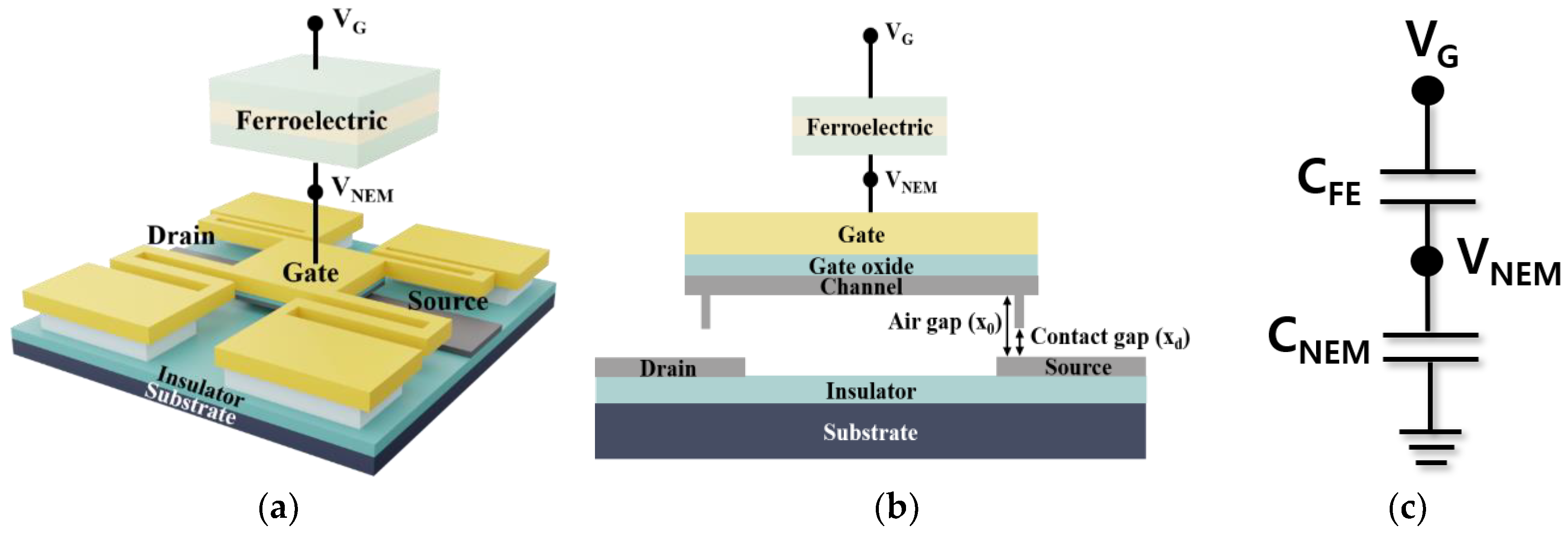
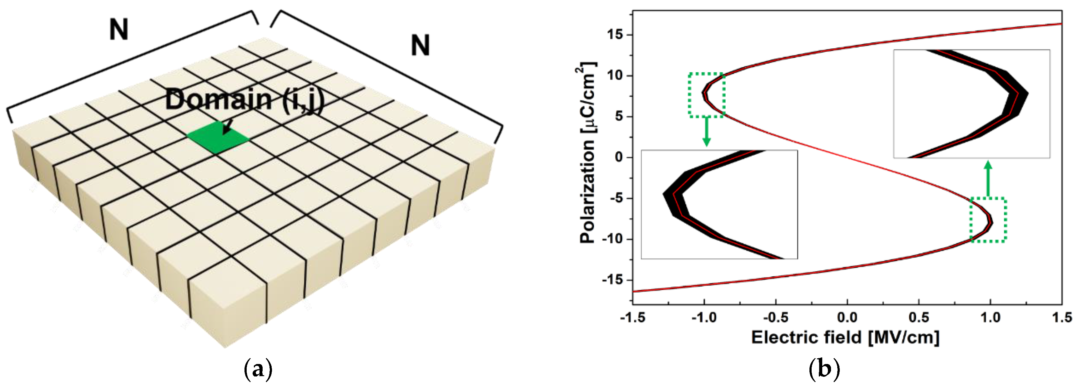
2. Simulation Methods

Figure 1a illustrates the isometric view of an NEM relay that is connected in series to a ferroelectric capacitor (i.e., NC + NEM relay). Because the bottom electrode of the ferroelectric capacitor is connected in series to the gate electrode of the NEM relay, the problem of a relatively large area (vs. the conventional NEM relay) may arise. This problem of the NC + NEM relay area can be alleviated by employing a ferroelectric capacitor on top of the CMOS circuit or in the CMOS back-end-of-line. Figure 1b shows the cross-sectional view along the channel of NC + NEM relay; Figure 1c illustrates the capacitive circuit of the NC + NEM relay. The ferroelectric capacitance ( C F E ) and the NEM relay capacitance ( C N E M ) are two representative capacitive components in the NC + NEM relay. There are three major forces that govern the behavior of the constituent NEM relay: (i) electrostatic force ( F e l e c ), (ii) adhesion force ( F a d ) and (iii) spring force ( F s p r i n g ). F e l e c and F a d induce physical contact between the conductive electrodes of the NEM relay, causing current to flow in it. In contrast, F s p r i n g induces the conductive electrodes to separate, preventing the current flow in the NEM relay. As illustrated in Figure 1a when the conductive electrodes of the NEM relay are physically separated, it is turned off, and there is negligible current flow through the channel. If a sufficient voltage is applied to the NEM relay so that the sum of F e l e c and F a d is stronger than F s p r i n g (i.e., F e l e c + F a d > F s p r i n g ), a physical contact is formed between the conductive electrodes. Therefore, current flows abruptly, and this phenomenon is known as pull-in. The voltage at which the pull-in state occurs is the pull-in voltage ( V p i ). In contrast, the conductive electrodes are physically separated when the sum of F e l e c and F a d becomes weaker than F s p r i n g (i.e., F e l e c + F a d < F s p r i n g ), preventing the abrupt current flow. This phenomenon is known as pull-out. Similarly, the voltage at which the pull-out state occurs is the pull-out voltage ( V p o ). In the present simulation, metal-to-metal electrodes were adopted to realize a low on–state resistance of the NEM relay [23]. Specifically, tungsten (W) was used for improved endurance and contact resistance stability [1]. F a d of metal-to-metal electrodes, which mainly originates from electron interaction, can be expressed using the following equation [23,24]:
F a d ( x ) = 2 γ A c ( x D 0 λ M 2 ) e x D 0 λ M ,
where γ is the surface energy density; A c is the contact area; D 0 is the average atomic distance when a physical contact is formed; λ M is the characteristic decay length, which is related to the Thomas–Fermi screening length [25], and x is the distance between the conductive electrode of the upper movable beam and the bottom fixed electrode. In this study, universal values of D 0 = 0.165 nm and λ M = 0.1 nm were employed to predict F a d between the metal-to-metal contact [23,24]. Concurrently, the NEM relay operates in the pull-in mode when the contact gap ( x d ) to air gap ( x 0 ) ratio is greater than 1/3 (i.e., x d / x 0 > 1/3) and in the non-pull-in mode when x d / x 0 < 1/3 [1]. It is known that an NEM relay consumes less switching energy when it operates in the pull-in mode (as opposed to the non-pull-in mode) [26]. Therefore, x d and x 0 were designed to operate the NEM relay in the pull-in mode. In the pull-in mode, V p i and V p o of the NEM relay are expressed as follows [27]:
V p i _ N E M = 8 k x 0 3 27 ε 0 A N
V p o _ N E M = 2 ( x 0 x d ) 2 ( k x d F a d ) ε 0 A N
where k is the spring constant; ε 0 is the dielectric constant of vacuum; and A N is the actuation area. Concurrently, the switching voltages (i.e., V p i and V p o ) of an NC + NEM relay change owing to the voltage amplification effect. Therefore, the pull-in/-out voltages of an NC + NEM relay (i.e., V p i _ N C N E M and V p o _ N C N E M ) are expressed as follows [5,6]:
V p i _ N C N E M = 2 α N E F F 3 3 α N E F F β N E F F ,
V p o _ N C N E M = α N E F F α P I V p o _ N E M β N E F F α P I 3 V p o _ N E M 3 ,
where α N E F F = α N     α F = ( k x 0 F a d ) / k ε 0 A N ( α t F E / A F E ) ;   β N E F F = β N β F = 1 / ( 2 k ( ε 0 A N ) 2 β t F E / A F E 3 ;   α P I = ( x 0 x d ) / ( ε 0 A N ) ; t F E and A F E are the thickness and area of the ferroelectric material, respectively; and α and β are the ferroelectric anisotropy constants. Figure 2a illustrates a ferroelectric material containing N × N domains (i.e., a multi-domain state). Recently, numerous experimental/theoretical studies have suggested that the polarization-switching kinetics of HfO2-based ferroelectric materials are not explained by the Kolmogorov-Avrami-Ishibashi (KAI) model, which is commonly adopted for elucidating the polarization-switching kinetics of perovskite-structured ferroelectric materials. The KAI model suggests that the switching times of ferroelectric materials are determined by the lateral domain wall expansion and predicts an exponential relationship between the switched polarization and the pulse width [28,29]. However, most of the HfO2-based ferroelectric materials possess a polycrystalline structure, whose grain boundaries are known to hinder the lateral domain wall expansion [13]. In addition, a logarithmic relationship between the switched polarization and the pulse width of a HfO2-based ferroelectric is observed experimentally, which is not explained by the KAI model [29]. Therefore, the polarization-switching kinetics of HfO2-based ferroelectrics have been extensively explained by the nucleation-limited-switching (NLS) model, [21,29,30] instead of using a conventional KAI model. The NLS assumes that ferroelectric materials are composed of elementary regions, where each region has an independent coercive field (Ec) and a remnant polarization (Pr) with a Gaussian distribution [21,31,32]. Based on a simple two-dimensional (2D) multi-domain Landau-Khalatnikov (L-K) equation considering NLS, the relationship between the polarization and the electric field of each domain can be expressed as follows [32]:
E F E = α i , j P i , j + β i , j P i , j 3 ,
where i and j are the locations of the domains, E F E is the electric field applied to the ferroelectric material, and P is the polarization. Thus, the overall polarization of the ferroelectric material can be obtained by averaging the P-values of all domains as follows [32]:
P = 1 N × N i j P i , j .
To model the intrinsic randomness of the HfO2-based ferroelectric material due to the grain size and crystallite orientation fluctuations, it was assumed that α and β of each domain have a Gaussian distribution with a mean value μ and standard deviation σ [13,32]. For simplicity, only the variation in α was considered in this study. The mean values of the ferroelectric anisotropy parameters (i.e., α and β ) were derived from the single-domain L-K equation as a function of remnant polarization ( P r ) and coercive field ( E c ) as follows [33]:
α = 3 3 E c 2 P r ,   β = 3 3 E c 2 P r 3 .
Subsequently, α of each domain was generated from the MATLAB function, normrnd. The baseline NEM relay and the ferroelectric capacitor were designed using the device parameters summarized in Table 1. Note that Young’s modulus (E) and spring constant (k) were obtained from previous works [34,35]. Figure 2b illustrates the P-E curve of the multi-domain ferroelectric material. The black curve represents the P-E curves of each domain, and the red curve is the P-E curve of the overall ferroelectric.

3. Results and Discussion
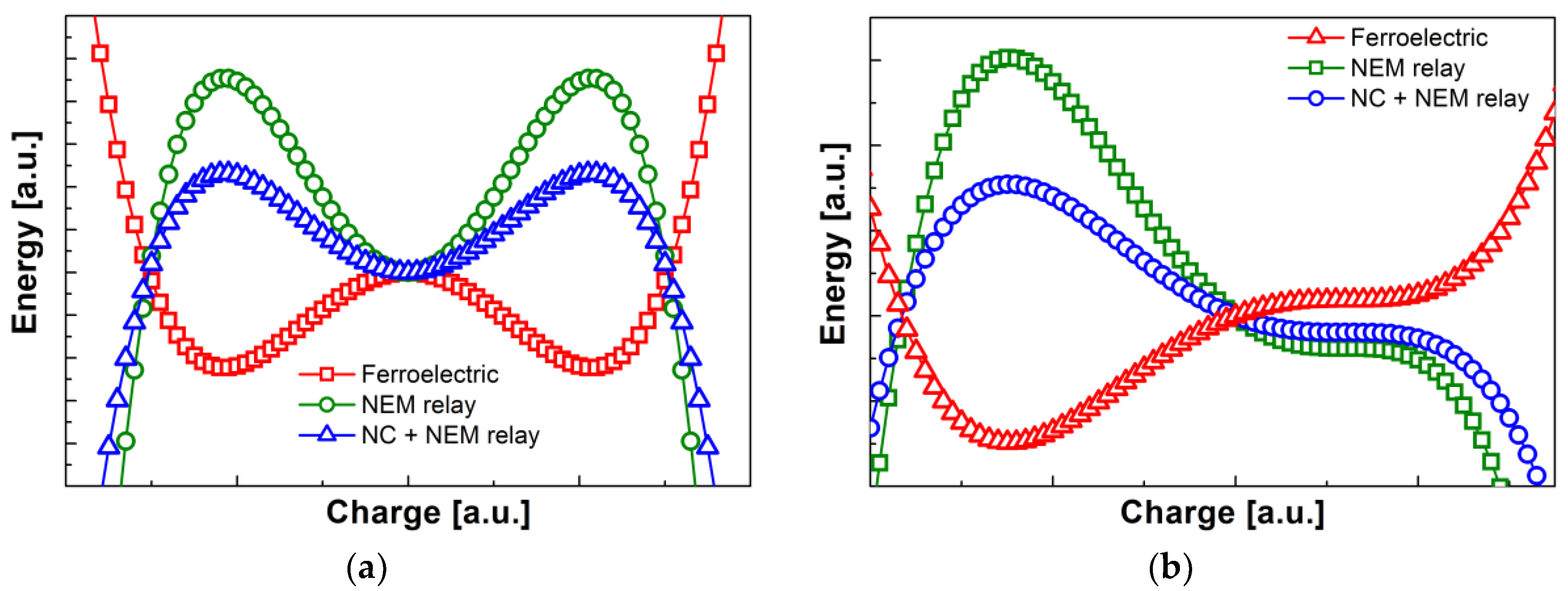
3.1. Single-Domain

Before exploring the electrical characteristics of the NEM relay with the multi-domain ferroelectric material, an NEM relay with a single-domain ferroelectric material were examined initially. In a single-domain ferroelectric, it is assumed that the polarization in the ferroelectric material is uniform; and, thus, the relation between the electric field and the polarization of the overall ferroelectric material is expressed as below:
E F E = α P + β P 3
where α and β are as given in Equation (8). To demonstrate the impact of the ferroelectric capacitor on the NEM relay, the energy landscapes of the ferroelectric capacitor ( U F ), NEM relay ( U N ) and NC + NEM relay ( U F N ) are illustrated in Figure 3. Herein, U F , U N and U F N are as follows:
U F = 1 2 α F Q 2 + 1 4 β F Q 4 V F Q ,
U N = 1 2 α N Q 2 1 4 β N Q 4 V N Q ,
U F N = 1 2 α N E F F Q 2 1 4 β N E F F Q 4 V F N Q ,
where V F , V N , V F N and Q are the voltages applied to the ferroelectric capacitor, NEM relay, NC + NEM relay and charge, respectively. Figure 3a shows the energy landscapes in the equilibrium state (i.e., voltage = 0 V). In contrast, Figure 3b illustrates the energy landscapes of ferroelectric capacitor, NEM and NC + NEM relays when the pull-in voltage is applied. The pull-in voltages of the NEM and NC + NEM relays are as expressed in Equations (2) and (4), respectively. As indicated in Figure 3a, the energy landscapes of the NEM relay and the ferroelectric capacitor have opposite shapes. Depending on the values of α N E F F and β N E F F , the energy landscape of the NC + NEM relay can be categorized into two types. If α N E F F and β N E F F are positive, the NC + NEM relay operates as a conventional NEM relay, which is called the “effective NEM relay mode.” In contrast, if α N E F F   and   β N E F F   are   negative , the NC + NEM relay operates as a ferroelectric capacitor, which is called the “effective FE mode.” [5] Previously, it was theoretically found that the operating voltage of an NC + NEM relay could be lowered compared to that of the conventional NEM relay by operating it in the “effective NEM relay mode” [5]. In this study, we designed the device design parameters (e.g., L b e a m , x 0 , t F E and A F E ) to operate the NC + NEM relay in the effective NEM relay mode. As illustrated in Figure 3a, the energy landscape of the NC + NEM relay has the same shape as that of the NEM relay. Note that the maxima in the energy landscape of the NC + NEM relay are much lower than that of the conventional NEM relay. Therefore, the pull-in/-out state of the NC + NEM relay could be achieved at a much lower voltage compared to the NEM relay. Specifically, the pull-in/-out voltages of the NC + NEM relay were 0.8159 V/0.0285 V and the pull-in/-out voltages of the NEM relay were 1.6319 V/0.7601 V, respectively.

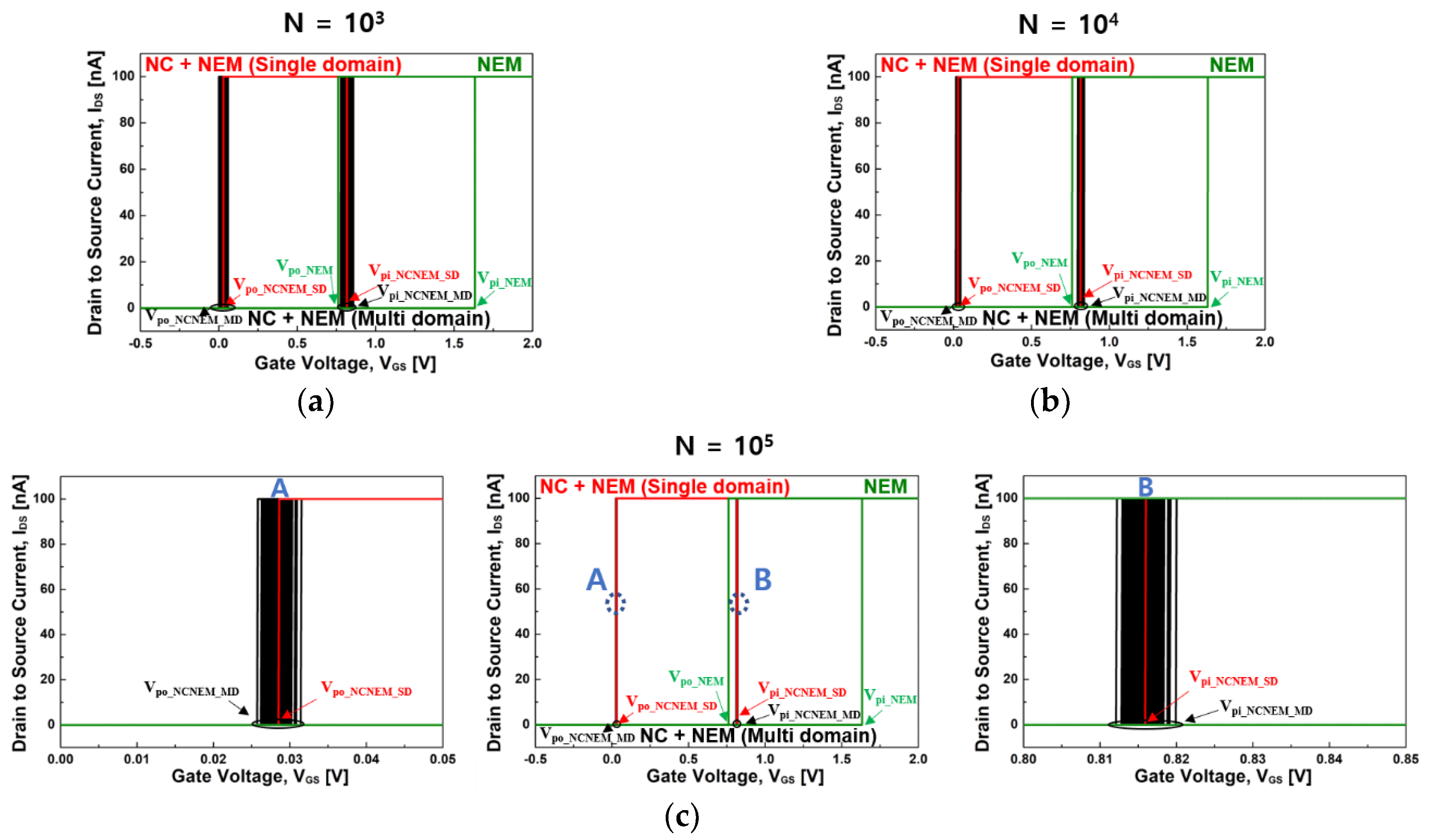
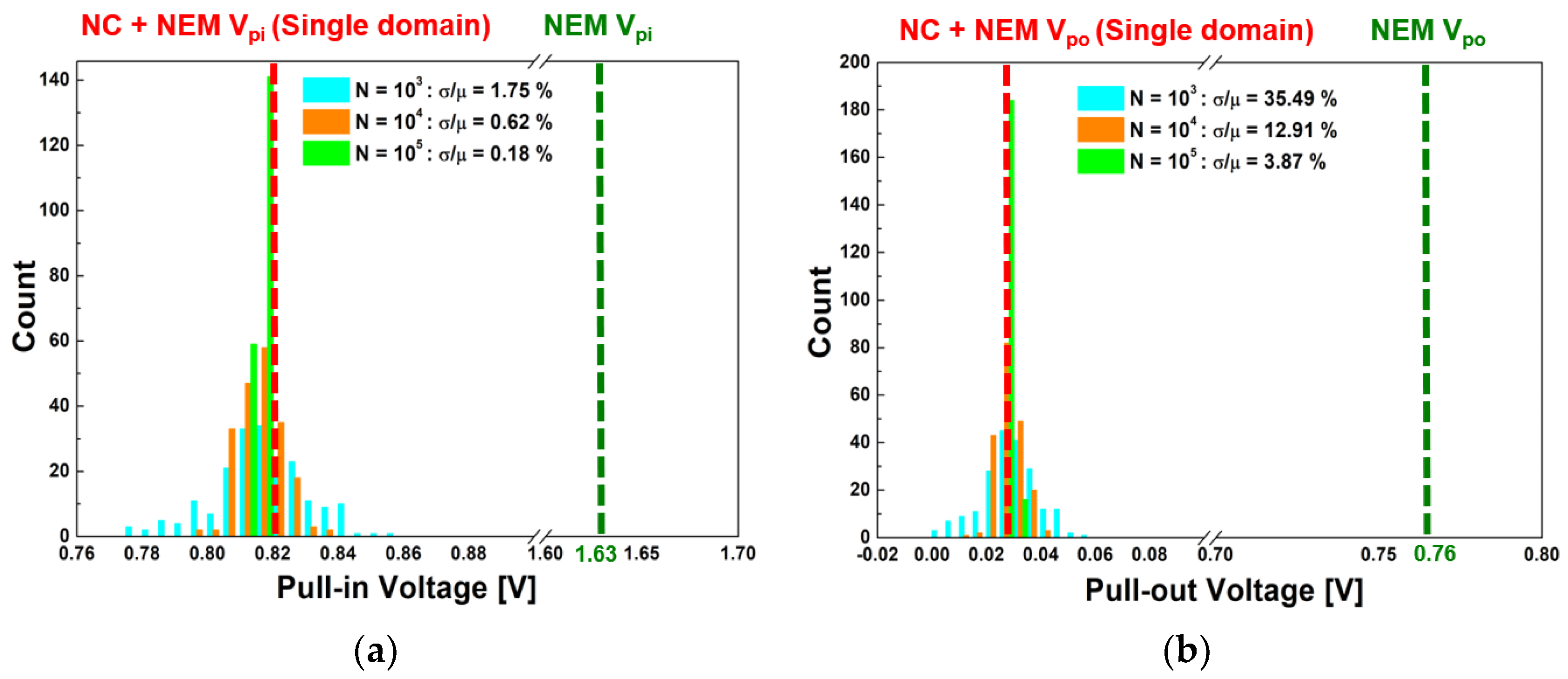
3.2. Multi-Domain: Domain Number (N) Change

We first explored the electrical characteristics of the NEM relay with the multi-domain ferroelectric material by modulating the number of domains while maintaining the domain inhomogeneity (i.e., σ = 0.4 α ), to analyze the corresponding impact. The number of domains was initially set as follows. Several studies have shown that the average grain size of HfO2-based ferroelectrics is 5–20 nm [18,36]. In addition, it was found that the domain size is generally smaller than the grain size [37]. Therefore, the number of ferroelectric domains was approximated by dividing the ferroelectric area by the domain area (i.e., 1.6 μ m 2 /160 nm 2   10 4 ) . Subsequently, by modulating the number of domains, the electrical characteristics of the NEM relay with the multi-domain ferroelectric material were observed. Figure 4 illustrates the simulated input transfer curves (i.e., I D S vs. V G S ) of the NEM relay, NEM relay with the single-domain ferroelectric material and NEM relay with the multi-domain ferroelectric material containing various number of domains. Herein, the input transfer curve of 200 samples of the NEM relay with the multi-domain ferroelectric material are illustrated. The red/black curve represents the input transfer curve of the NEM relay with the single-/multi-domain ferroelectric, respectively. Moreover, the green curve represents the input transfer curve of the conventional NEM relay. Note that a compliance current of 100 nA was set to prevent welding-induced stiction between the contact electrodes due to the Joule heating generated from the high current flow [38]. Figure 5 indicates that the switching voltage of the NEM relay with the single-/multi-domain ferroelectric material (i.e., V p i _ N C N E M and V p o _ N C N E M ) is much lower than that of the conventional NEM relay, owing to voltage amplification. In addition, a variation in the switching voltage in the NEM relay with the multi-domain ferroelectric material is observed, which is due to the intrinsic randomness of the polycrystalline HfO2-based ferroelectric material. Figure 5 presents the distributions of the switching voltages of the NEM relay and the NEM relay with the single-/multi-domain ferroelectric material. When the number of domains is 10 3 , 10 4 and 10 5 , the average of the switching voltages is slightly different. Therefore, for a more accurate comparison, the relative standard deviation (i.e., σ/μ) was obtained and comparisons made. The results indicate that the switching voltage distribution of the NEM relay with the multi-domain ferroelectric material becomes larger as the number of domains decreases. Herein, some samples of the NEM relay with the multi-domain ferroelectric material were observed to have a pull-out voltage close to 0 V. When the pull-out voltage is less than 0 V, the NEM relay will not be turned off even if Vgs = 0 V. Therefore, special care must be taken to avoid this problem. In brief, in order to eliminate the variation of switching voltage in NC + NEM relay, it is most ideal to use a single domain ferroelectric material. However, if inevitable, it is important to reduce/minimize the number of domains in multi-domain ferroelectric material.

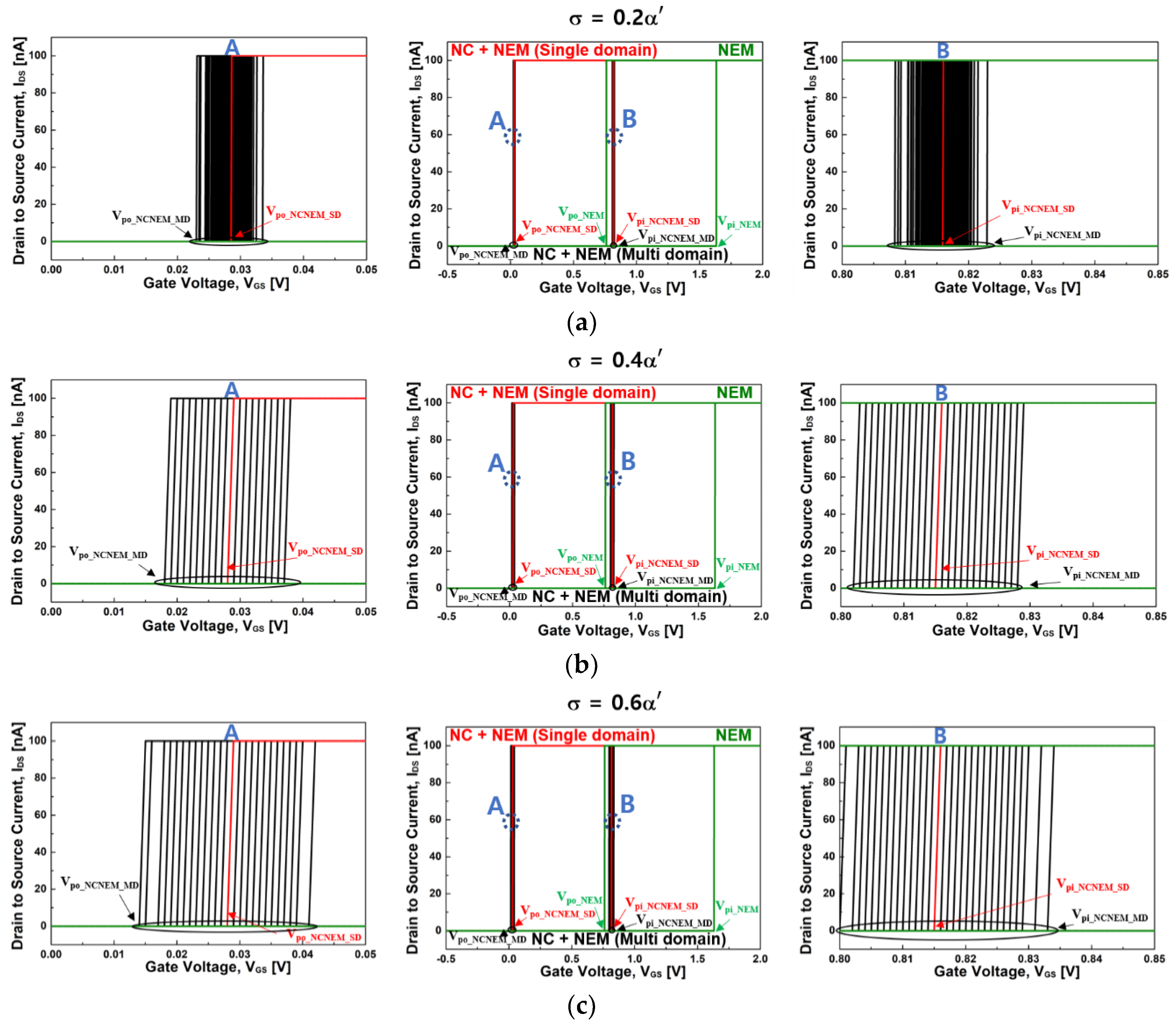
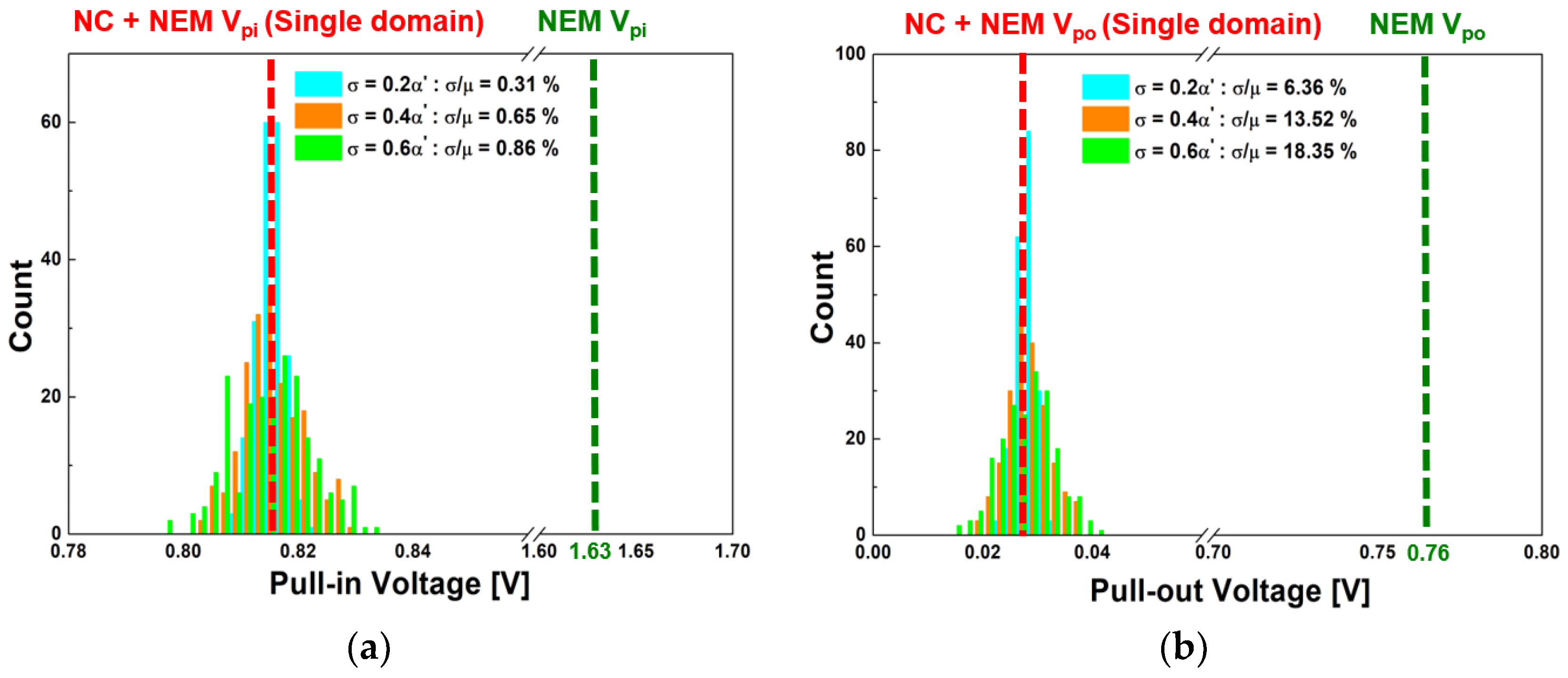
3.3. Multi-Domain: Domain Inhomogeneity (σ) Change

Next, we examined the electrical properties of the NEM relay with the multi-domain ferroelectric material by modulating the domain inhomogeneity while maintaining the number of domains (i.e., N = 10 4 ) to analyze the corresponding effects. Specifically, domain inhomogeneity was changed to σ = 0.2 α , σ = 0.4 α and σ = 0.6 α . Domain inhomogeneity represents the differences in the ferroelectricity of each domain. Therefore, a large domain inhomogeneity indicates that the inhomogeneity of the ferroelectric properties of each domain (i.e., P r and E c ) is large. Considering that α can be expressed as a function of P r and E c (see Equation (8)), the inhomogeneity of α increases with increasing domain inhomogeneity, which results in a switching voltage variation. Figure 6 displays the simulated input transfer curves of the NEM relay, NEM relay with a single domain ferroelectric material and NEM relay with the multi-domain ferroelectric material with various domain inhomogeneities (i.e., σ = 0.2 α , 0.4 α and 0.6 α ). The red/black curve illustrates the simulated input transfer curve of the NEM relay with the single-/multi-domain ferroelectric material, respectively. Moreover, the green curve represents the input transfer curve of the conventional NEM relay. Figures indicate that the switching voltages of the NEM relay with the multi-domain ferroelectric material is still lower than that of the conventional NEM relay, regardless of the domain inhomogeneity. Figure 7 shows the switching voltages distribution of the NEM relay and NEM relays with the single-domain ferroelectric and multi-domain ferroelectrics. A larger switching voltage distribution of the NEM relay with the multi-domain ferroelectric material was observed as the domain inhomogeneity increased. Specifically, the relative standard deviations of V p i _ N C N E M and V p o _ N C N E M increased by 0.31%/6.36%, 0.65%/13.52% and 0.86%/18.35% as the domain inhomogeneity increased by σ = 0.2 α , σ = 0.4 α and σ = 0.6 α , respectively.

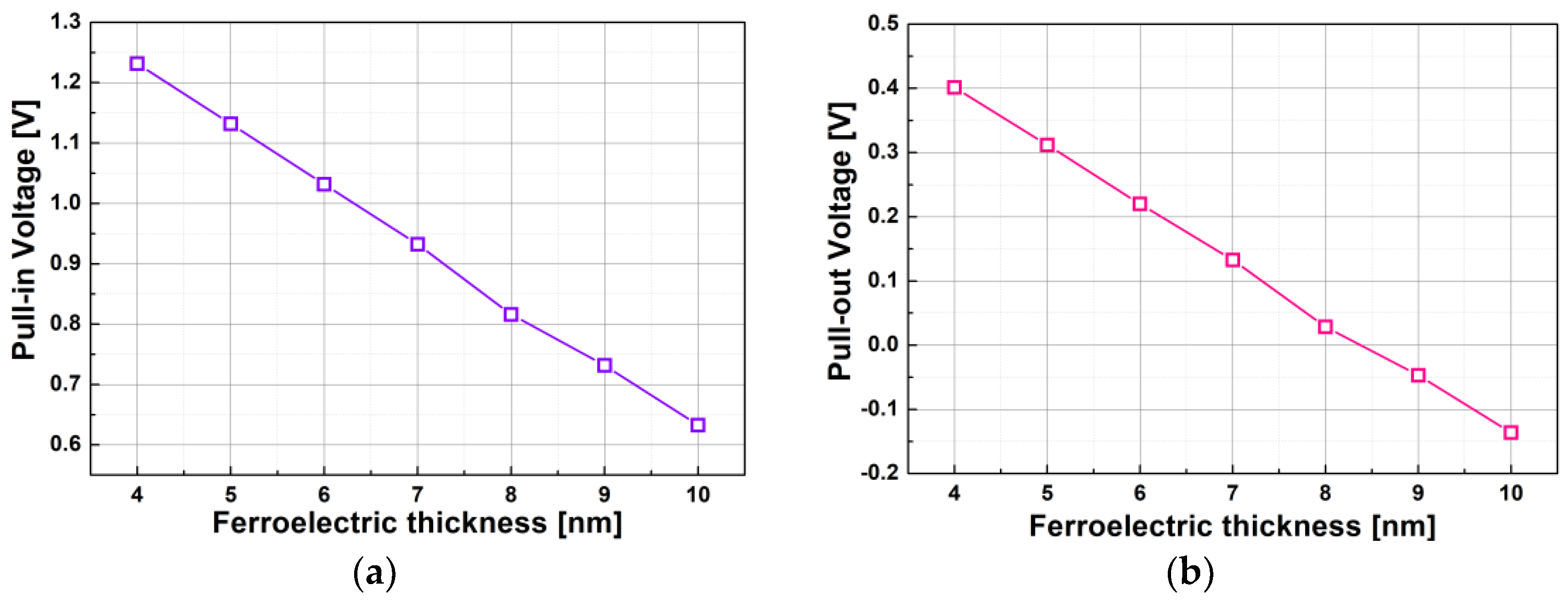
3.4. Multi-Domain: Ferroelectric Thickness (tFE) Variation

Finally, we compared the electrical characteristics of the NEM relay with the multi-domain ferroelectric material by changing the ferroelectric thickness ( t F E ), which can be modulated by the fabrication process. Herein, the number of ferroelectric domains and the domain inhomogeneity were assumed to be constant, while the t F E was varied to solely analyze the effect of the t F E on the electrical characteristics of the NEM relay with the multi-domain ferroelectric material. Figure 8 illustrates the switching voltages of the NEM relay with the multi-domain ferroelectric material with several t F E . The figures indicate that the pull-in/-out voltage of the NEM relay with the multi-domain ferroelectric material decreases as t F E increases. The voltage amplification at the internal gate (Av) owing to the negative capacitance effect is given as below [17]:
A v = V i n t V G = | C F E | | C F E | C N E M
Herein, the magnitude of the ferroelectric negative capacitance, | C F E | , can be expressed as follows [17,39]:
C F E = Q V F E = 1 t F E ( α + 3 β Q 2 )     2 3 3 P r t F E E c
The equation above suggests that | C F E | is proportional to P r / t F E E c . It is well-known that HfO2-based ferroelectric materials coexist in tetragonal, monoclinic and orthorhombic phases. Among them, ferroelectricity is known to originate from the orthorhombic phases [40]. It was investigated and found that the portion of monoclinic phase increases with increasing t F E , thus decreasing the portion of the orthorhombic phase. Therefore, the remnant polarization ( P r ) decreases with increasing t F E , owing to the decreased portion of the orthorhombic phase [40,41,42]. Concurrently, t F E -dependent coercive fields ( E c ) of perovskite materials have been extensively studied (i.e., E c ~ t F E 2 / 3 ) [43]. In contrast, E c of HfO2-based ferroelectric is found not to present any ferroelectric thickness dependence [30,43]. In summary, P r decreases and E c remains unchanged with an increase in t F E . This results in a decrease in C F E with increasing t F E , as per Equation (14). Thus, a larger t F E results in increased A v as per Equation (13). Therefore, the switching voltages of the NEM relay with the multi-domain ferroelectric decrease with increasing t F E , as illustrated in Figure 8. Notably, if the number of domains and the domain inhomogeneity vary simultaneously with t F E , relatively large variations in the switching voltages of the NEM relay with the multi-domain ferroelectric material will occur.

4. Conclusions

In this study, the effects of a multi-domain HfO2-based ferroelectric material on the electrical properties of an NEM relay were theoretically investigated. Switching voltage variations in the NEM relay with the multi-domain ferroelectric material were observed, which were due to the randomness of the polycrystalline HfO2-based ferroelectric material. Even considering the variation in the switching voltages, the switching voltages of the NEM relay with the multi-domain ferroelectric material were smaller than those of the conventional NEM relay. It was observed that the switching voltage variations decreased with increasing the number of domains and decreasing domain inhomogeneity. In addition, it was observed that the switching voltages decreased with increasing ferroelectric thickness because the voltage amplification increased with the ferroelectric thickness.

Author Contributions

Conceptualization, C.Y. and C.S.; methodology, C.Y.; software, C.Y.; validation, C.Y. and C.S.; formal analysis, C.Y.; investigation, C.Y.; resources, C.Y.; data curation, C.Y. and C.S.; writing—original draft preparation, C.Y.; writing—review and editing, C.S.; visualization, C.Y.; supervision, C.S.; project administration, C.S.; funding acquisition, C.S. All authors have read and agreed to the published version of the manuscript.

Funding

This study was supported by the National Research Foundation of Korea (NRF) through a grant funded by the Korean government (MSIP) (No. 2020R1A2C1009063).

Conflicts of Interest

The authors declare no conflict of interest.

References

  1. Peschot, A.; Qian, C.; Liu, T.-J.K. Nanoelectromechanical Switches for Low-Power Digital Computing. Micromachines 2015, 6, 1046–1065. [Google Scholar] [CrossRef]
  2. Pott, V.; Kam, H.; Nathanael, R.; Jeon, J.; Alon, E.; Liu, T.-J.K. Mechanical Computing Redux: Relays for Integrated Circuit Applications. IEEE Proc. 2010, 98, 2076–2094. [Google Scholar] [CrossRef]
  3. Kwon, H.S.; Kim, S.K.; Choi, W.Y. Monolithic Three-Dimensional 65-nm CMOS-Nanoelectromechanical Reconfigurable Logic for Sub-1.2-V Operation. IEEE Electron Device Lett. 2017, 38, 1317–1320. [Google Scholar] [CrossRef]
  4. Osoba, B.; Saha, B.; Dougherty, L.; Edgington, J.; Qian, C.; Niroui, F.; Lang, J.H.; Bulovic, V.; Wu, J.; Liu, T.-J.K. Sub-50 mV NEM relay operation enabled by self-assembled molecular coating. In Proceedings of the 2016 IEEE International Electron Devices Meeting (IEDM), San Francisco, CA, USA, 3–7 December 2016. [Google Scholar]
  5. Masuduzzaman, M.; Alam, M.A. Effective Nanometer Airgap of NEMS Devices Using Negative Capacitance of Ferroelectric Materials. Nano Lett. 2014, 14, 3160–3165. [Google Scholar] [CrossRef] [PubMed]
  6. Choe, K.; Shin, C. Adjusting the Operating Voltage of an Nanoelectromechanical Relay Using Negative Capacitance. IEEE Trans. Electron Devices 2017, 64, 5270–5273. [Google Scholar] [CrossRef]
  7. Salahuddin, S.; Datta, S. Use of negative capacitance to provide voltage amplification for low power nanoscale devices. Nano Lett. 2008, 8, 405–410. [Google Scholar] [CrossRef] [PubMed]
  8. Khan, A.I.; Chatterjee, K.; Wang, B.; Drapcho, S.; You, L.; Serrao, C.; Bakaul, S.R.; Ramesh, R.; Salahuddin, S. Negative capacitance in a ferroelectric capacitor. Nat. Mater. 2015, 14, 182–186. [Google Scholar] [CrossRef]
  9. Khan, A.I.; Bhowmik, D.; Yu, P.; Kim, S.J.; Pan, X.; Ramesh, R.; Salahuddin, S. Experimental evidence of ferroelectric negative capacitance in nanoscale heterostructures. Appl. Phys. Lett. 2011, 99, 113501. [Google Scholar] [CrossRef] [Green Version]
  10. Jo, J.; Choi, W.Y.; Park, J.-D.; Shim, J.W.; Yu, H.-Y.; Shin, C. Negative Capacitance in Organic/Ferroelectric Capacitor to Implement Steep Switching MOS Devices. Nano Lett. 2015, 15, 4553–4556. [Google Scholar] [CrossRef]
  11. Ku, H.; Shin, C. Transient Response of Negative Capacitance in P(VDF0.75-TrFE0.25) Organic Ferroelectric Capacitor. IEEE J. Electron Devices Soc. 2017, 5, 232–236. [Google Scholar] [CrossRef]
  12. Appleby, D.J.R.; Ponon, N.K.; Kwa, K.S.K.; Zou, B.; Petrov, P.K.; Wang, T.; Alford, N.M.; O’Neill, A. Experimental observation of negative capacitance in ferroelectrics at room temperature. Nano Lett. 2014, 14, 3864–3868. [Google Scholar] [CrossRef]
  13. Hoffmann, M.; Pešić, M.; Chatterjee, K.; Khan, A.I.; Salahuddin, S.; Slesazeck, S.; Schroeder, U.; Mikolajick, T. Direct Observation of Negative Capacitance in Polycrystalline Ferroelectric HfO2. Adv. Funct. Mater. 2016, 26, 8643–8649. [Google Scholar] [CrossRef]
  14. Kwon, D.; Chatterjee, K.; Tan, A.J.; Yadav, A.K.; Zhou, H.; Sachid, A.B.; Reis, R.D.; Hu, C.; Salahuddin, S. Improved Subthreshold Swing and Short Channel Effect in FDSOI n-Channel Negative Capacitance Field Effect Transistors. IEEE Electron Device Lett. 2018, 39, 300–303. [Google Scholar] [CrossRef]
  15. Zhang, Z.; Xu, G.; Zhang, Q.; Hou, Z.; Li, J.; Kong, Z.; Zhang, Y.; Xiang, J.; Xu, Q.; Wu, Z.; et al. FinFET With Improved Subthreshold Swing and Drain Current Using 3-nm Ferroelectric Hf0.5Zr0.5O2. IEEE Electron Device Lett. 2019, 40, 367–370. [Google Scholar] [CrossRef]
  16. Zhou, J.; Han, G.; Li, J.; Liu, Y.; Peng, Y.; Zhang, J.; Sun, Q.-Q.; Zhang, D.W.; Hao, Y. Effects of the Variation of VGS Sweep Range on the Performance of Negative Capacitance FETs. IEEE Electron Device Lett. 2018, 39, 618–621. [Google Scholar] [CrossRef]
  17. Pahwa, G.; Dutta, T.; Agarwal, A.; Chauhan, Y.S. Designing Energy Efficient and Hysteresis Free Negative Capacitance FinFET with Negative DIBL and 3.5X Ion using Compact Modeling Approach. In Proceedings of the European Solid-State Device Research Conference (ESSDERC), Lausanne, Switzerland, 12–15 September 2016; pp. 41–46. [Google Scholar]
  18. Kim, K.D.; Park, M.H.; Kim, H.J.; Kim, Y.J.; Moon, T.; Lee, Y.H.; Hyun, S.D.; Gwon, T.; Hwang, C.S. Ferroelectricity in undoped-HfO2 thin films induced by deposition temperature control during atomic layer deposition. J. Mater. Chem. C 2016, 4, 6864–6872. [Google Scholar] [CrossRef]
  19. Choe, K.; Shin, C. Impact of negative capacitance on the energy-delay property of an electromechanical relay. Jpn. J. Appl. Phys. 2019, 58, 051003. [Google Scholar] [CrossRef]
  20. Tan, Y.; Zhang, J.; Wu, Y.; Wang, C.; Koval, V.; Shi, B.; Ye, H.; McKinnon, R.; Viola, G.; Yan, H. Unfolding grain size effects in barium titanate ferroelectric ceramics. Sci. Rep. 2015, 5, 9953. [Google Scholar] [CrossRef] [Green Version]
  21. Gong, N.; Sun, X.; Jiang, H.; Chang-Liao, K.S.; Xia, Q.; Ma, T.P. Nucleation limited switching (NLS) model for HfO2-based metal-ferroelectric-metal (MFM) capacitors: Switching kinetics and retention characteristics. Appl. Phys. Lett. 2018, 112, 262903. [Google Scholar] [CrossRef]
  22. Zhu, L.; You, J.H.; Chen, J.; Yeo, C. Molecular dynamics simulations of ferroelectric domain formation by oxygen vacancy. J. Phys. D Appl. Phys. 2018, 51, 185303. [Google Scholar] [CrossRef]
  23. Chen, I.-R.; Qian, C.; Yablonovitch, E.; Liu, T.-J.K. Nanomechanical Switch Designs to Overcome the Surface Adhesion Energy Limit. IEEE Electron Device Lett. 2015, 36, 963–965. [Google Scholar] [CrossRef]
  24. Pawashe, C.; Lin, K.; Kuhn, K.J. Scaling Limits of Electrostatic Nanorelays. IEEE Trans. Electron Devices 2013, 60, 2936–2942. [Google Scholar] [CrossRef]
  25. Rose, J.H.; Ferrante, J.; Smith, J.R. Universal Binding Energy Curves for Metals and Bimetallic Interfaces. Phys. Rev. Lett. 1981, 47, 675–678. [Google Scholar] [CrossRef]
  26. Qian, C.; Peschot, A.; Connelly, D.J.; Liu, T.-J.K. Energy-Delay Performance Optimization of NEM Logic Relay. In Proceedings of the 2015 IEEE International Electron Devices Meeting (IEDM), Washington, DC, USA, 7–9 December 2015. [Google Scholar]
  27. Kam, H.; Liu, T.-J.K.; Stojanovi, V.; Markovic, D.; Alon, E. Design, Optimization, and Scaling of MEM Relays for Ultra-Low-Power Digital Logic. IEEE Trans. Electron Devices 2011, 58, 236–250. [Google Scholar] [CrossRef] [Green Version]
  28. Orihara, H.; Hashimoto, S.; Ishibashi, Y. A thoery of D-E hystersis loop Based on the Avrami Model. J. Phys. Soc. Jpn. 1994, 63, 1031–1035. [Google Scholar] [CrossRef]
  29. Mueller, S.; Summerfelt, S.R.; Muller, J.; Schroeder, U.; Mikolajick, T. Ten-Nanometer Ferroelectric Si:HfO2 Films for Next-Generation FRAM Capacitors. IEEE Electron Device Lett. 2012, 33, 1300–1302. [Google Scholar] [CrossRef]
  30. Toriumi, A.; Xu, L.; Mori, Y.; Tian, X.; Lomenzo, P.D.; Mulaosmanovic, H.; Mikolajick, T.; Schroeder, U. Material perspectives of HfO2-based ferroelectric films for device applications. In Proceedings of the 2019 IEEE International Electron Devices Meeting (IEDM), San Francisco, CA, USA, 7–11 December 2019. [Google Scholar]
  31. Tagantsev, A.K.; Stolichnov, I.; Setter, N.; Cross, J.S.; Tsukada, M. Non-Kolmogorov-Avrami switching kinetics in ferroelectric thin films. Phys. Rev. B 2002, 66, 214109. [Google Scholar] [CrossRef]
  32. Chang, P.; Zhang, Y.; Du, G.; Liu, X. Experiment and modeling of dynamical hysteresis in thin film ferroelectrics. Jpn. J. Appl. Phys. 2020, 59, SGGA07. [Google Scholar] [CrossRef]
  33. Khandelwal, S.; Duarte, J.P.; Khan, A.I.; Salahuddin, S.; Hu, C. Impact of Parasitic Capacitance and Ferroelectric Parameters on Negative Capacitance FinFET Characteristics. IEEE Electron Device Lett. 2017, 38, 142–144. [Google Scholar] [CrossRef]
  34. Kam, H. Micro-Relay Technology for Energy Efficient Integrated Circuits; Springer: Berlin/Heidelberg, Germany, 2015. [Google Scholar]
  35. Choi, W.Y. Design and scaling of nano-electro-mechanical non-volatile memory (NEMory) cells. Curr. Appl. Phys. 2010, 10, 311–316. [Google Scholar] [CrossRef]
  36. Onaya, T.; Nabatame, T.; Sawamoto, N.; Ohi, A.; Ikeda, N.; Chikyow, T.; Ogura, A. Improvement in ferroelectricity of HfxZr1−xO2 thin films using ZrO2 seed layer. Appl. Phys. Express 2017, 10, 081501. [Google Scholar] [CrossRef]
  37. Hyun, S.D.; Park, H.W.; Kim, Y.J.; Park, M.H.; Lee, Y.H.; Kim, H.J.; Kwon, Y.J.; Moon, T.; Kim, K.D.; Lee, Y.B.; et al. Dispersion in Ferroelectric Switching Performance of Polycrystalline Hf0.5Zr0.5O2 Thin Films. ACS Appl. Mater. Interfaces 2018, 10, 35374–35384. [Google Scholar] [CrossRef] [PubMed]
  38. Osoba, B.; Saha, B.; Almeida, S.F.; Patil, J.; Brandt, L.E.; Roots, M.E.D.; Acosta, E.; Wu, J.; Liu, T.-J.K. Variability Study for Low-Voltage Microelectromechanical Relay Operation. IEEE Trans. Electron Devices 2018, 65, 1529–1534. [Google Scholar] [CrossRef]
  39. Zhou, J.; Peng, Y.; Han, G.; Li, Q.; Liu, Y.; Zhang, J.; Liao, M.; Sun, Q.-Q.; Zhang, D.W.; Zhou, Y.; et al. Hysteresis Reduction in Negative Capacitance Ge PFETs Enabled by Modulating Ferroelectric Properties in HfZrOx. IEEE J. Electron Devices Soc. 2018, 6, 41–48. [Google Scholar] [CrossRef]
  40. Park, M.H.; Kim, H.J.; Kim, Y.J.; Lee, W.; Moon, T.; Hwang, S.C. Evolution of phases and ferroelectric properties of thin Hf0.5Zr0.5O2 films according to the thickness and annealing temperature. Appl. Phys. Lett. 2013, 102, 242905. [Google Scholar] [CrossRef]
  41. Yurchuk, E.; Müller, J.; Knebel, S.; Sundqvist, J.; Graham, A.P.; Melde, T.; Schröder, U.; Mikolajick, T. Impact of layer thickness on the ferroelectric behaviour of silicon doped hafnium oxide thin films. Thin Solid Films 2013, 533, 88–92. [Google Scholar] [CrossRef]
  42. Park, M.H.; Kim, H.J.; Kim, Y.J.; Lee, W.; Moon, T.; Kim, K.D.; Hwang, C.S. Study on the degradation mechanism of the ferroelectric properties of thin Hf0.5Zr0.5O2 films on TiN and Ir electrodes. Appl. Phys. Lett. 2014, 105, 072902. [Google Scholar] [CrossRef]
  43. Migita, S.; Ota, H.; Yamada, H.; Shibuya, K.; Sawa, A.; Toriumi, A. Polarization switching behavior of Hf–Zr–O ferroelectric ultrathin films studied through coercive field characteristics. Jpn. J. Appl. Phys. 2018, 57, 04FB01. [Google Scholar] [CrossRef]
Figure 1. (a) Isometric view of negative capacitance (NC) + nanoelectromechanical (NEM) relay. Note that NEM relay is connected in series to ferroelectric capacitor; (b) cross-sectional view along the channel of NC + NEM relay when it is turned off; (c) capacitive circuit schematic of NC + NEM relay.
Electronics 09 01208 g001
Figure 2. (a) Illustration of ferroelectric material containing N × N domains; (b) simulated polarization vs. electric field of multi-domain ferroelectric material. Black/red curve represents polarization vs. electric field of each domain/overall ferroelectric material, respectively.
Electronics 09 01208 g002
Figure 3. (a) Simulated energy landscapes of ferroelectric capacitor, NEM relay and NC + NEM relay in equilibrium state; (b) simulated energy landscapes of ferroelectric capacitor, NEM relay and NC + NEM relay when pull-in voltage is applied.
Electronics 09 01208 g003
Figure 4. Simulated drain to source current vs. gate voltage of NEM relay, NEM relay with single-domain ferroelectric and NEM relay with multi-domain ferroelectric containing (a) 103 domains, (b) 104 domains and (c) 105 domains. Note that the pull-in/-out voltage of NEM relay (i.e., Vpi_NEM and Vpo_NEM), pull-in/-out voltage of NEM relay with single-domain ferroelectric material (Vpi_NCNEM_SD and Vpo_NCNEM_SD) and pull-in/-out voltage of NEM relay with multi-domain ferroelectric material (Vpi_NCNEM_MD and Vpo_NCNEM_MD) are indicated in figure.
Electronics 09 01208 g004
Figure 5. Distribution of (a) pull-in voltage and (b) pull-out voltage for an NEM relay, NEM relay with a single-domain ferroelectric and 200 samples of an NEM relay with a multi-domain ferroelectric. Variation of pull-in/-out voltage increases as the number of domain decreases.
Electronics 09 01208 g005
Figure 6. Simulated drain to source current vs. gate voltage of NEM relay, NEM relay with single-domain ferroelectric and NEM relay with multi-domain ferroelectric with various domain inhomogeneities (i.e., (a) σ = 0.2 α ; (b) σ = 0.4 α and (c) σ = 0.6 α ).
Electronics 09 01208 g006
Figure 7. Distribution of (a) pull-in voltage and (b) pull-out voltage for NEM relay, NEM relay with single-domain ferroelectric and 200 samples of NEM relay with multi-domain ferroelectric. Note that variation in pull-in/-out voltage increases as domain inhomogeneity increases.
Electronics 09 01208 g007
Figure 8. Estimated (a) pull-in voltage and (b) pull-out voltage of NEM relay with multi-domain ferroelectric with various ferroelectric thicknesses. Note that pull-in/-out voltage is decreased with increasing ferroelectric thickness.
Electronics 09 01208 g008
Table 1. Modeling parameters.
SymbolDescriptionUnitValue
A N Actuation area μ m 2 400
A c Contact area μ m 2 100
x d Contact gapnm40
x 0 Air gapnm70
L b e a m Beam lengthμm10
t b e a m Beam thicknessnm100
W b e a m Beam widthμm20
t F E Ferroelectric thicknessnm8
A F E Ferroelectric area μ m 2 1.6
P r Remnant polarizationμC/ cm 2 13.5
E c Coercive fieldMV/cm1
ΓSurface energy densityJ/ m 2 3.5
EYoung’s modulus
(poly-Si0.4Ge0.6) 34
GPa145
kSpring constant
(=32E W b e a m t b e a m 3 / L b e a m 3 ) 35
N/m92.8

