Article

THz CMOS On-Chip Antenna Array Using Defected Ground Structure

Department of Electronic Engineering, Sogang University, Seoul 04107, Korea
*
Author to whom correspondence should be addressed.
Electronics 2020, 9(7), 1137; https://doi.org/10.3390/electronics9071137
Submission received: 1 July 2020 / Revised: 10 July 2020 / Accepted: 11 July 2020 / Published: 13 July 2020
(This article belongs to the Collection Millimeter and Terahertz Wireless Communications)

Abstract

:
In this paper, we design a THz CMOS on-chip patch antenna with defected ground structure (DGS) and utilize it to implement a broadband and high gain on-chip antenna array. It is verified from the simulation that the DGS not only can increase the gain and bandwidth of the antenna element, but also can increase the isolation between the antenna elements in the on-chip array. Therefore, it allows the design of the compact 1 × 2 and 2 × 2 on-chip antenna array with high gain and broad bandwidth. The element spacing and feedline structures of the antenna array are designed and optimized by the simulations. The designed antenna element, and 1 × 2 and 2 × 2 antenna arrays are fabricated in a commercial 65 nm CMOS process. In the on-wafer measurement, they exhibit an antenna gain of 3.1 dBi, 7.2 dBi, and 8.2 dBi with a bandwidth of 14.0%, 21.3%, and 28.0% for the reflection coefficient less than −10 dB, respectively, at 300 GHz. This result corresponds to very good performance compared to the reported THz CMOS on-chip antenna array. Therefore, the designed CMOS on-chip antenna element and array using DGS in this work can be effectively applied to build low-cost and high performance THz systems, because they can be fully implemented in a conventional CMOS process without requiring any additional processes or manufacturing techniques.

1. Introduction

Recently, there has been extensive research on semiconductor-based terahertz (THz) integrated circuits (ICs) for imaging sensors, radars, and wireless communications [1,2]. Especially, silicon (Si) CMOS technology is accepted as a good choice for low-cost THz ICs, because of its performance advancement by the device scaling and the high density integration of analog and digital circuits in a low-cost process. In THz Si CMOS ICs, the antenna can also be integrated in Si substrate, which can minimize the performance degradation caused by interconnections with an off-chip antenna and achieve a highly repeatable performance [3,4]. Therefore, a CMOS on-chip antenna is essential to the low-cost and high performance THz circuits and systems.
The THz CMOS on-chip antenna has been developed in a number of types of backside and frontside radiation. The first is to use a slot or dipole antenna to radiate an electromagnetic wave into the backside through Si substrate. However, it entails a low radiation efficiency due to the loss of Si substrate. In order to alleviate this problem, several solutions have been proposed such as a Si lens on the backside of the substrate [5,6,7] and a localized backside etching (LBE) technique which locally removes the lossy Si substrate underneath the antenna [8].
However, this problem can be simply mitigated by using the frontside radiation in which the lossy Si substrate is shielded by the ground plane consisting of bottom metal layers in the CMOS process. A CMOS on-chip patch, a typical antenna for the frontside radiation, utilizes top metal layers for radiation and bottom metal layers as a ground plane. However, the dielectric layers between the top and bottom metal layers are usually very thin in the commercial CMOS process, which in general entails narrow bandwidth, low gain, and low radiation efficiency [4,9]. To increase the gain and radiation of the frontside radiating antenna, a dielectric resonator was attached on top of the CMOS on-chip patch in [10]. The defected ground structure (DGS) was introduced by the authors to increase the radiation resistance and bandwidth of the CMOS on-chip patch antenna [11].
However, single on-chip antenna still exhibits a limited gain performance at THz frequencies. Therefore, it is required to array the on-chip antenna elements in a large size for higher directivity and gain. There have been several researches in CMOS on-chip antenna array. In [8], a 1 × 4 array was designed at 245 GHz in the SiGe BiCMOS process using a dipole antenna with an LBE technique, which allows the gain increase of 7 dB (according to the simulation). However, the feedline structure using Wilkinson power dividers occupies a large chip area. The backward radiating slot antenna was designed at 260 GHz in a 65 nm CMOS process, and eight element antennas were arrayed with the hemispherical Si lens attached on the back to enhance the directivity in [12].
In this work, we design a compact THz CMOS on-chip patch antenna using a DGS and parasitic patch to obtain the broadband and high gain antenna element. Then, it is extended to 1 × 2 and 2 × 2 antenna array with determining the optimum element spacing. The low-loss feedline structures are also designed for broadband impedance matches. It is shown from the simulations that the DGS proposed in this work can reduce the coupling between the antenna elements in the array, so that it allows a high gain of on-chip antenna array under a compact area. This paper presents the simulation and measurement results of a THz on-chip antenna element and arrays fabricated in a 65 nm CMOS process. The measured performance is compared to the previously reported THz CMOS on-chip antenna.

2. Design of THz CMOS On-Chip Antenna Array

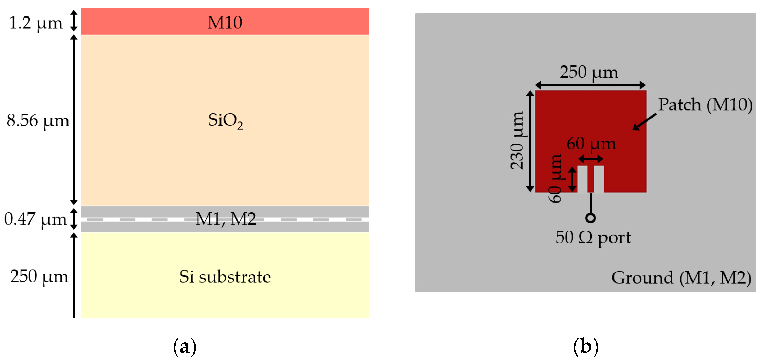
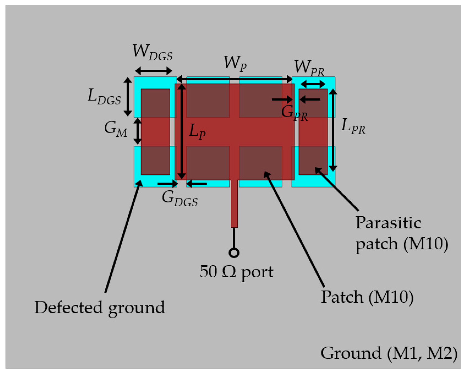
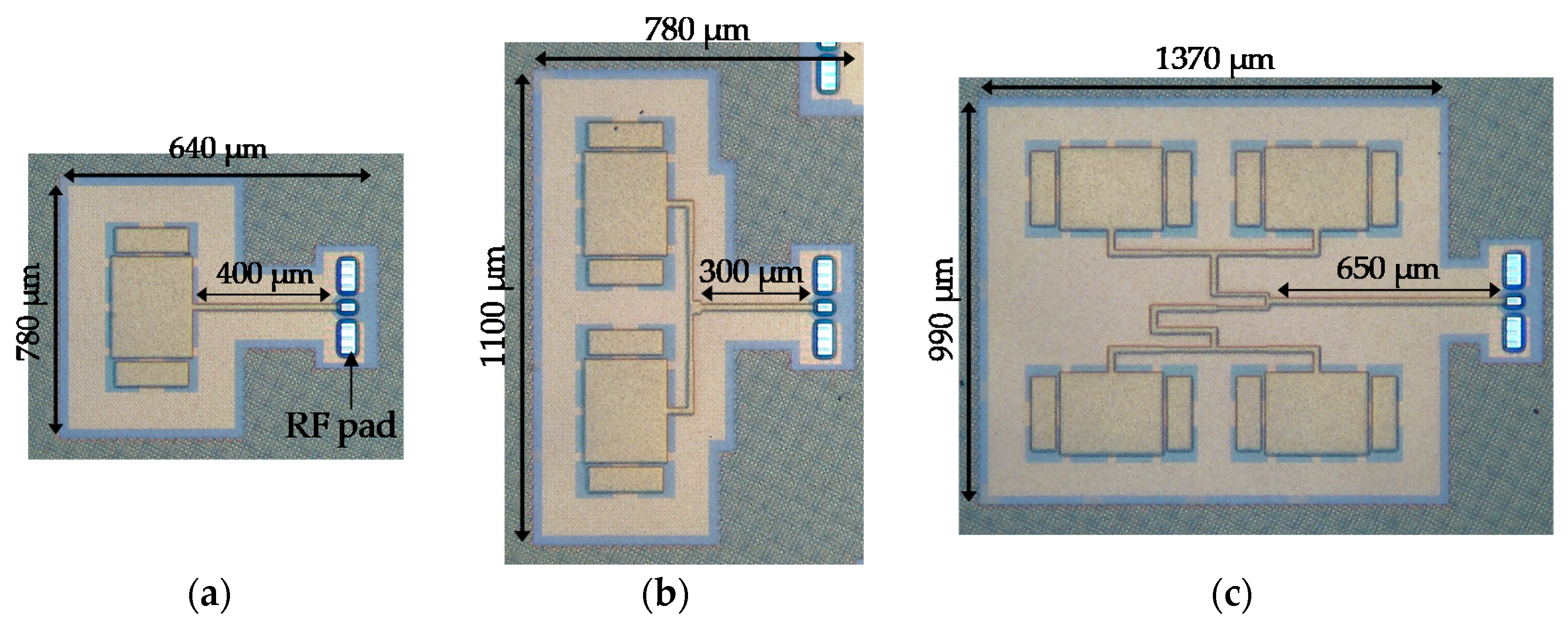
2.1. THz CMOS On-Chip Antenna Element

We design a high gain and compact on-chip antenna in a commercial CMOS process which will be used as an antenna element in the on-chip antenna array. Figure 1 shows the back-end-of-line (BEOL) structure of a commercial 65 nm CMOS process in which the frontside metal and dielectric layers are utilized in the design of a frontside radiating antenna element. The designed on-chip patch antenna consists of a top metal layer (M10) as a radiating patch and two lower-most metal layers (M1 and M2) as a ground plane, so that the thickness of the dielectric substrate in between can be maximized to allow for high radiation resistance. It can enable the CMOS on-chip patch antenna to have improved bandwidth and radiation efficiency [11,13].
Figure 1b shows the reference patch antenna designed at a center frequency of 300 GHz, where an inset feed is employed for the input impedance match. Its simulated performance will be compared later with the proposed antenna with the DGS. In the simulation, the reference patch exhibits a very limited bandwidth (1.3%) with a gain of 3.6 dBi caused by the very thin metal and dielectric layers in the BEOL structure of the CMOS process. Therefore, there should be research in improving the bandwidth and gain of a CMOS on-chip antenna at THz frequencies.
Recently, the V-shaped patch antenna with the DGS was proposed by the authors, improving the performance of the CMOS on-chip antenna [11]. The slots in the DGS allow the leakage of the electromagnetic wave into the silicon substrate, which increases the radiation resistance and thus the bandwidth and efficiency of the antenna. In addition, the leakage waves through the DGS can increase the antenna gain. They are partly reflected by the backside metal ground and can be added in phase with the frontside radiating waves from the patch antenna. If the thickness of the silicon substrate is about odd multiples of the quarter-wave length at operating frequency, it can result in an increase in the antenna gain. The bandwidth was further improved by the V-shaped patch in M9 with slots and the resonant patch in M10.
In this work, we re-design the patch antenna with the DGS to be applied for the antenna array. For this purpose, the radiating patch is implemented in the top layer of M10 instead of M9, and the V-shaped patch is replaced with a rectangular one with parasitic patches as shown in Figure 2. Two parasitic patches are placed in a close proximity to the radiating patch, so that they reduce the current density along the patch edges and improve the radiation efficiency. The length of the parasitic patches (LPR) can change the resonance frequency of the patch antenna and thus is carefully determined by the simulation. Despite the advantages of the DGS mentioned above, the leakage waves into the silicon substrate through the DGS can reduce the radiation efficiency due to the loss by the low-resistivity silicon substrate in the conventional CMOS process. Therefore, the DGS is carefully re-designed to provide the best performance in terms of the bandwidth and radiation efficiency. Table 1 shows the dimension of the re-designed patch antenna with the DGS at 300 GHz band.

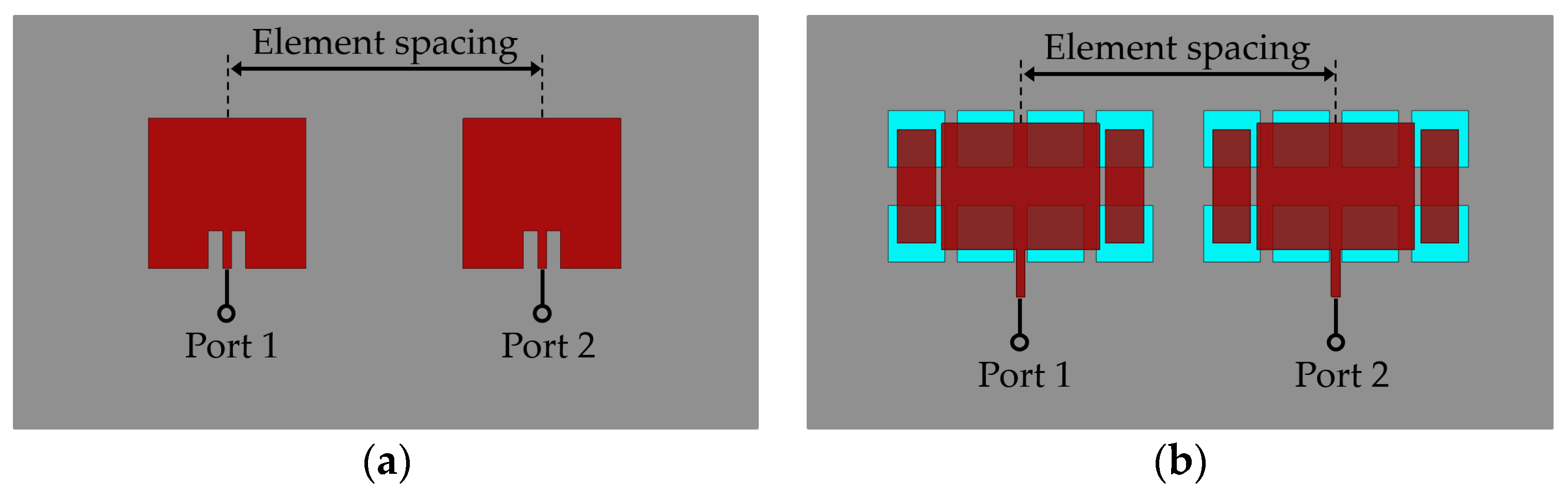
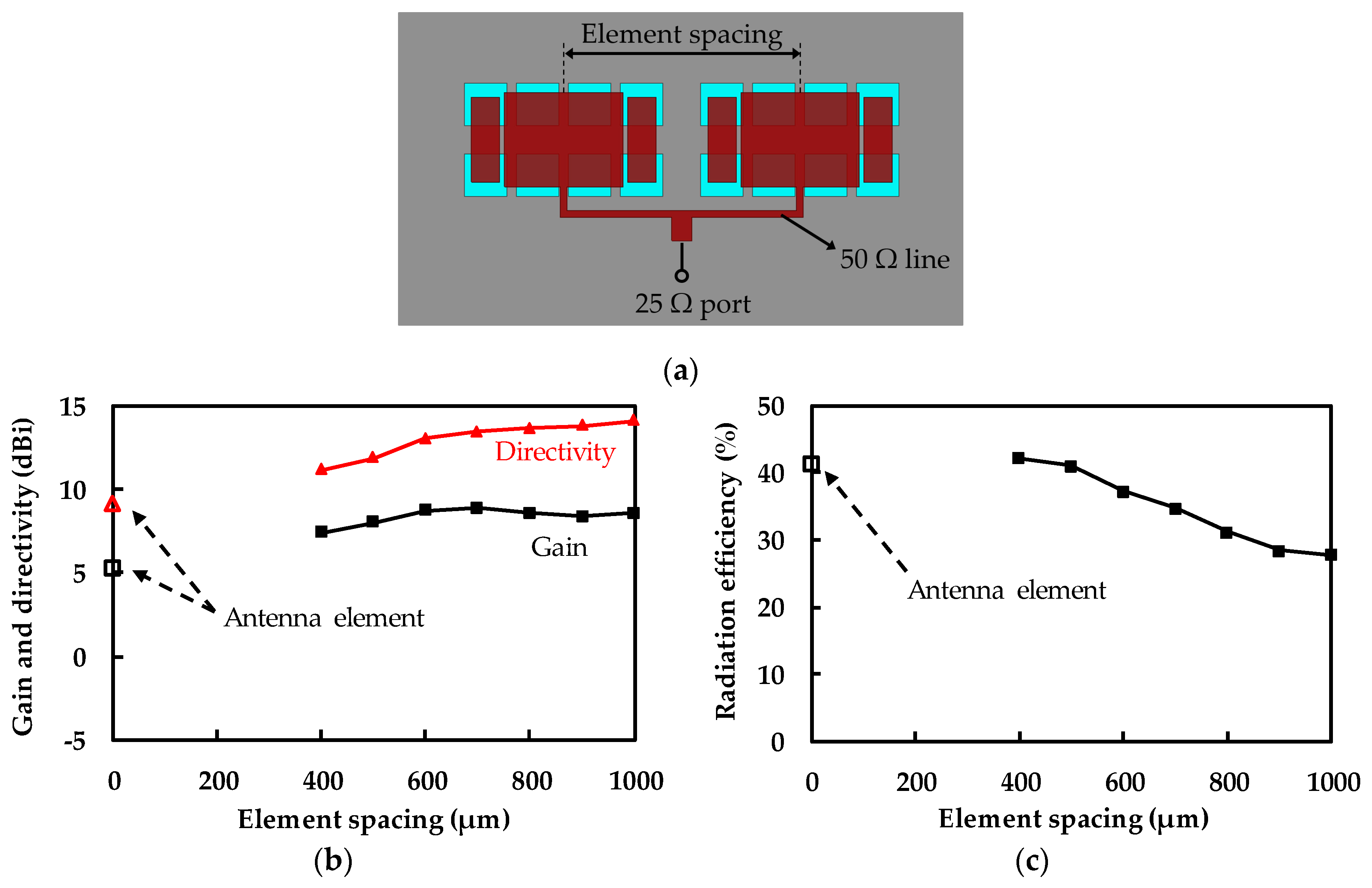
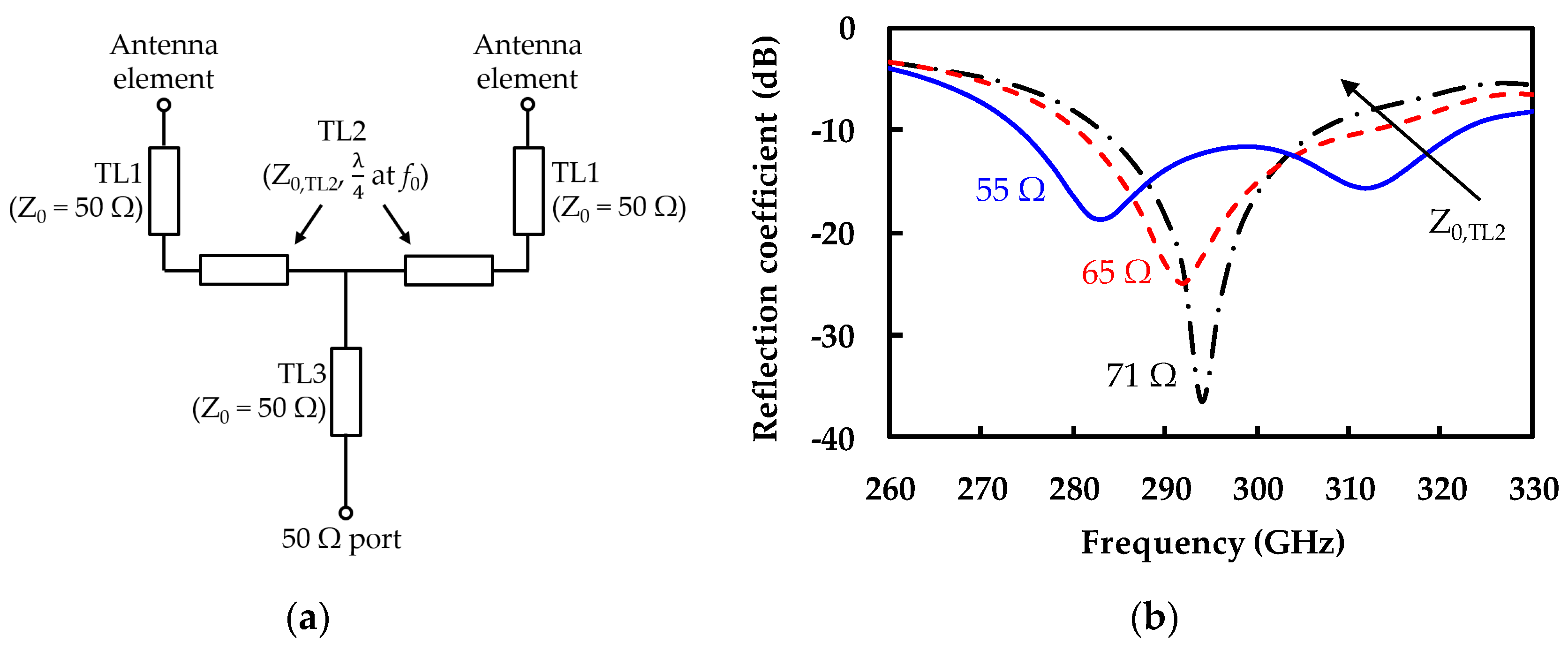
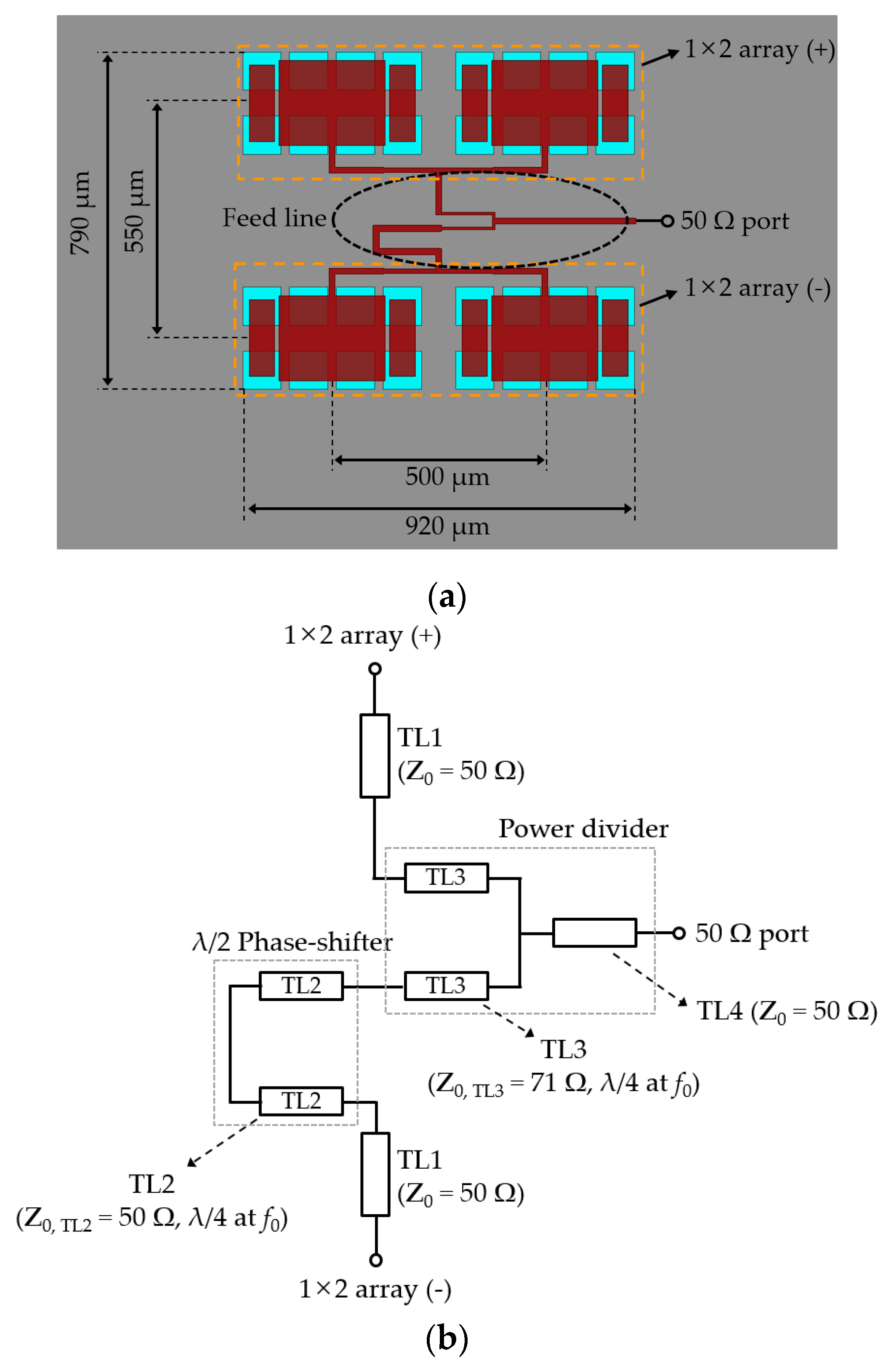
2.2. THz CMOS On-Chip Array

An antenna array can be implemented by placing antenna elements in a uniform spacing. In general, it is desirable to reduce the element spacing for the compact array. However, the close placement can increase the coupling between antenna elements due to the surface wave propagation. The coupling can deform the current distribution in each antenna element, which results in the performance degradation in the impedance matches and radiation efficiency [14]. Therefore, it is essential, especially in the CMOS on-chip array, to enhance the isolation between antenna elements. It is found from the simulations that the DGS can effectively reduce the coupling between antenna elements and thus be very beneficial for on-chip antenna array. In order to demonstrate this fact, we compare the simulated performance of the 1 × 2 arrays using the reference antenna elements of Figure 1b and the proposed antenna elements with the DGS of Figure 2. Figure 3 illustrates this simulation, where each antenna element is matched to 50 Ω. The minimum allowable element spacing is 300 μm and 400 μm in the array using a reference and proposed antenna element, respectively. Figure 4a shows the simulated coupling between two antenna elements (S21). As expected, the coupling increases as the element spacing decreases. This figure clearly shows that the DGS can reduce the coupling (by 6 dB at an element spacing of 400 μm), compared to the array using reference patch antenna. This effect is revealed in the simulated radiation efficiency of Figure 4b. The efficiency of the 1 × 2 antenna array using reference patches keeps decreasing when two antenna elements get closer, which is caused by the increased coupling. On the contrary, the 1 × 2 antenna array using the antenna element with the DGS maintains almost constant efficiency depending on the element spacing. It exhibits the radiation efficiency of 40.3% which corresponds to 3.6% points higher than those using the reference patch at the element spacing of 400 μm. Therefore, it is verified from the simulation that the DGS can reduce the coupling and thus enhance the radiation efficiency of the antenna array, so that it is beneficial for the design of a high efficiency on-chip antenna array with a compact area.
In order to determine the element spacing, we analyze the performance of the 1 × 2 antenna array using the proposed antenna with the DGS as shown in Figure 5a. The inputs of two antenna elements are simply connected with 50 Ω feedlines in microstrip and terminated with 25 Ω in order for the impedance match. In this way, the effect of the impedance mismatch on the performance can be ignored depending on the feedline length or element spacing. Figure 5b,c show the simulated gain, directivity, and radiation efficiency of the 1 × 2 array as a function of element spacing. As expected, directivity keeps increasing as element spacing increases. However, the radiation efficiency decreases with element spacing, which is caused by the increased loss of 50 Ω feedlines. In the results, the gain exhibits a maximum of 8.9 dBi at the element spacing of 700 μm. However, the side-lobes in the radiation pattern start to be generated from element spacing of 600 μm, which is undesirable in real applications of the antenna array and needs to be suppressed [15,16]. In this work, therefore, we selected the element spacing of 500 μm, considering the directivity, radiation efficiency, side-lobes, and chip size.
Next, we design the feedline structure for the input impedance match of the 1 × 2 antenna array using quarter-wave (λ/4) long lines with characteristic impedance of Z0,TL2, as depicted in Figure 6a. Figure 6b shows the simulated reflection coefficient as a function of Z0,TL2. At the center frequency, Z0,TL2 of 71 Ω provides the best impedance match. However, it allows very limited bandwidth of only 8.0% for the reflection coefficient less than −10 dB. Therefore, we selected Z0,TL2 of 55 Ω with the bandwidth of 15.3% while admitting some mismatches.
Finally, we design a 2 × 2 antenna array using the designed 1 × 2 arrays as shown in Figure 7a. Two 1 × 2 arrays should be fed with the signals with 180° phase difference, so that the electromagnetic fields radiated by each 1 × 2 array can add in phase in space. In this work, a half-wave (λ/2) long line with a characteristic impedance of 50 Ω is utilized as a 180° phase shifter and included in the feedline structure as shown in Figure 7b. The power divider is implemented using quarter-wave long lines with a characteristic impedance of 71 Ω.

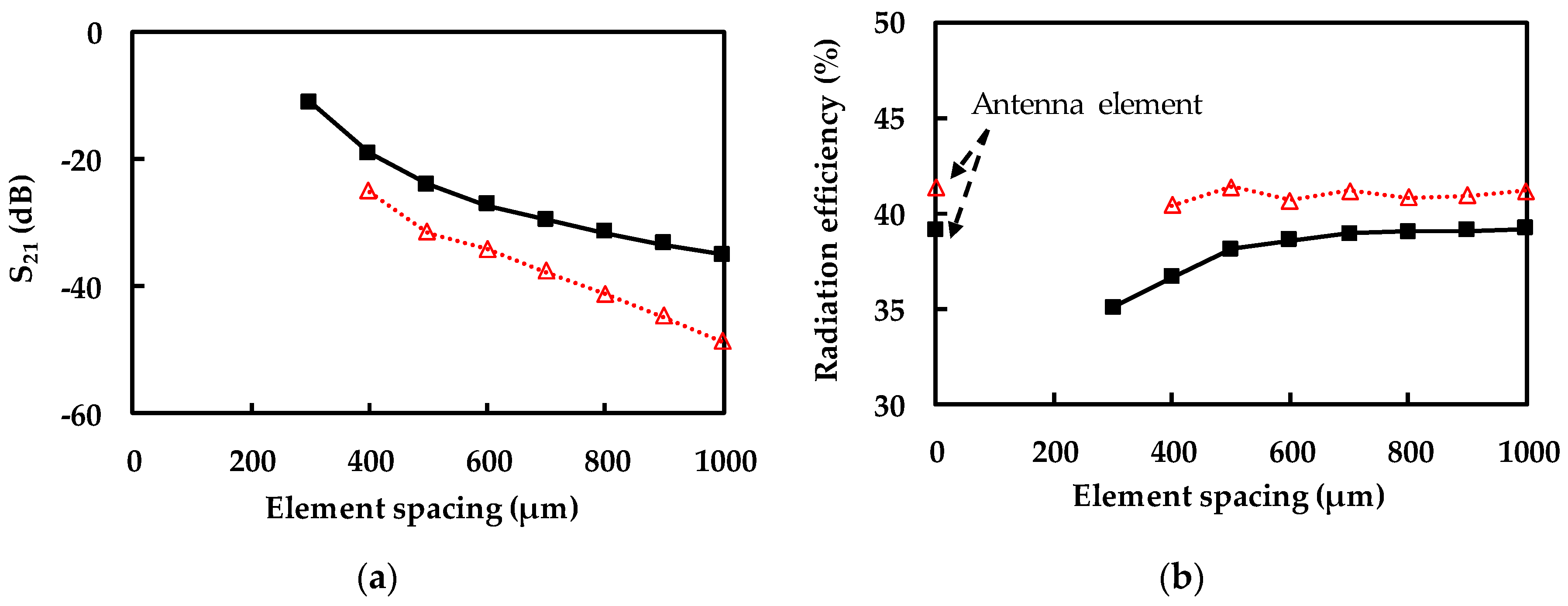
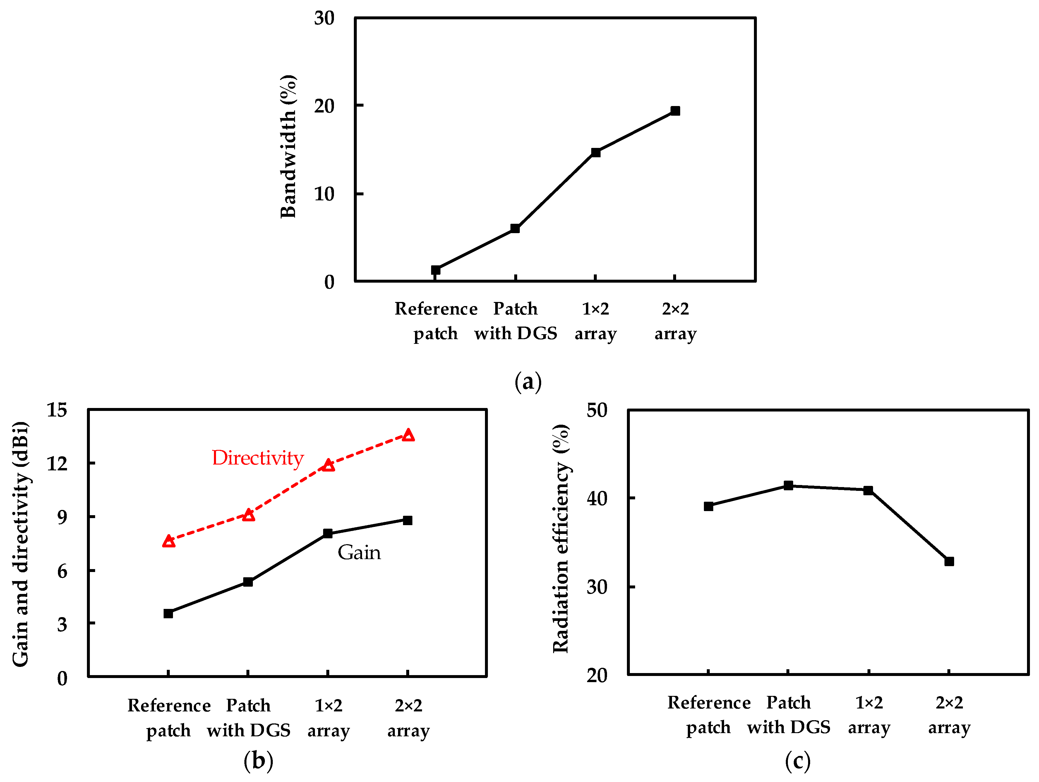
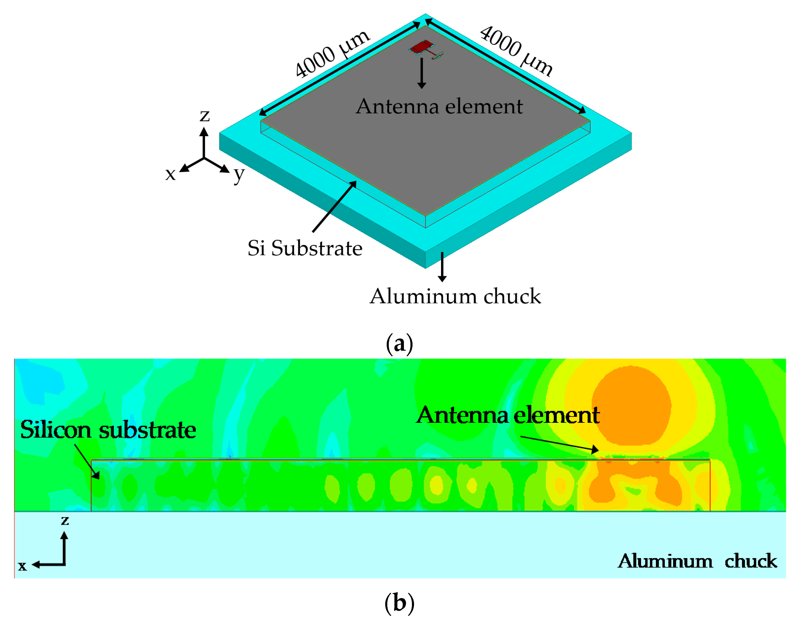
2.3. Simulation Results

Figure 8 shows the simulation results of the designed patch antenna with the DGS, 1 × 2 and 2 × 2 antenna arrays. The simulation result of the reference patch antenna is also included for comparison. The reference antenna exhibits very narrow bandwidth of only 1.3% (for the reflection coefficient less than −10 dB). The proposed patch antenna shows the improved bandwidth of 6.0% thanks to the DGS and parasitic resonant patches, as shown in Figure 8a. The bandwidth of 1 × 2 and 2 × 2 arrays further increases to 14.7% and 19.3%, respectively, which is made possible by the wideband feedline structure. Figure 8b shows that the directivity and gain are also improved by increasing the number of antenna elements in the array. The 1 × 2 antenna array achieves 2.7 dB higher directivity and gain than the antenna element. The radiation efficiency is 0.5% points less due to the feedline loss. However, the performance improvement slows down in the 2 × 2 array which shows 1.7 dB higher directivity than the 1 × 2 array, but the gain is improved by only 0.8 dB. It is caused by the increased loss by the very long lines in the feedline structure which reduces radiation efficiency by 8.0% points as shown in Figure 8c. Therefore, the number of antenna elements or array size in the CMOS on-chip antenna array can be limited by the loss in the feedline structure. Based on this result, we selected the maximum array size as 2 × 2 in this work.

3. Experimental Results

The designed antenna was fabricated in a commercial 65 nm CMOS process. Figure 9 shows the photograph of the fabricated CMOS on-chip antenna (antenna element, 1 × 2 array, and 2 × 2 array). We measured the antenna performance by on-wafer probing in which the metal probes can affect the radiation performance of the on-chip antenna [11]. In order to reduce this effect, very long 50 Ω lines (length >300 μm (~0.7λ at 300 GHz) ) are inserted between the antenna input and RF probe pad.

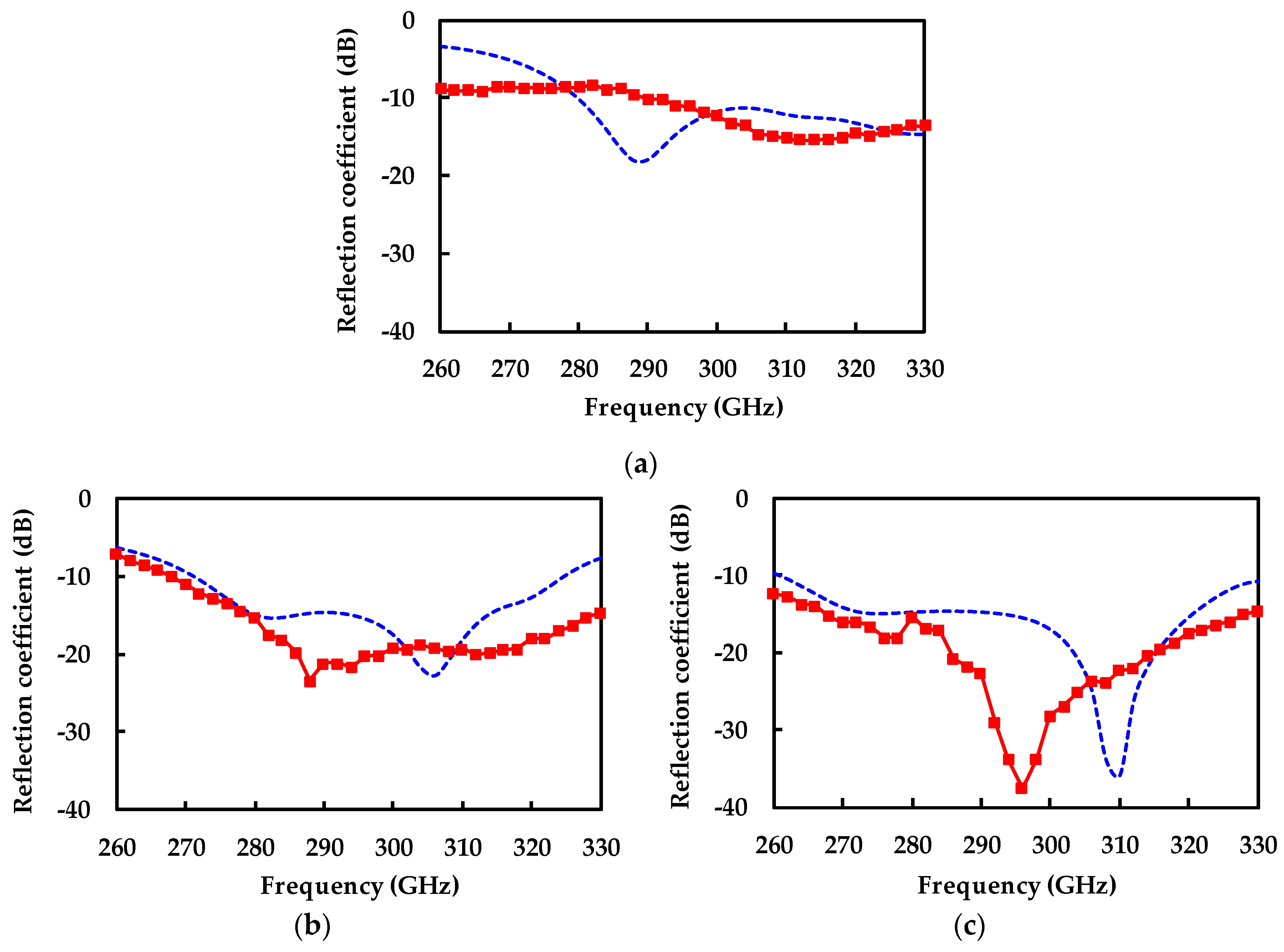
3.1. Reflection Coefficient
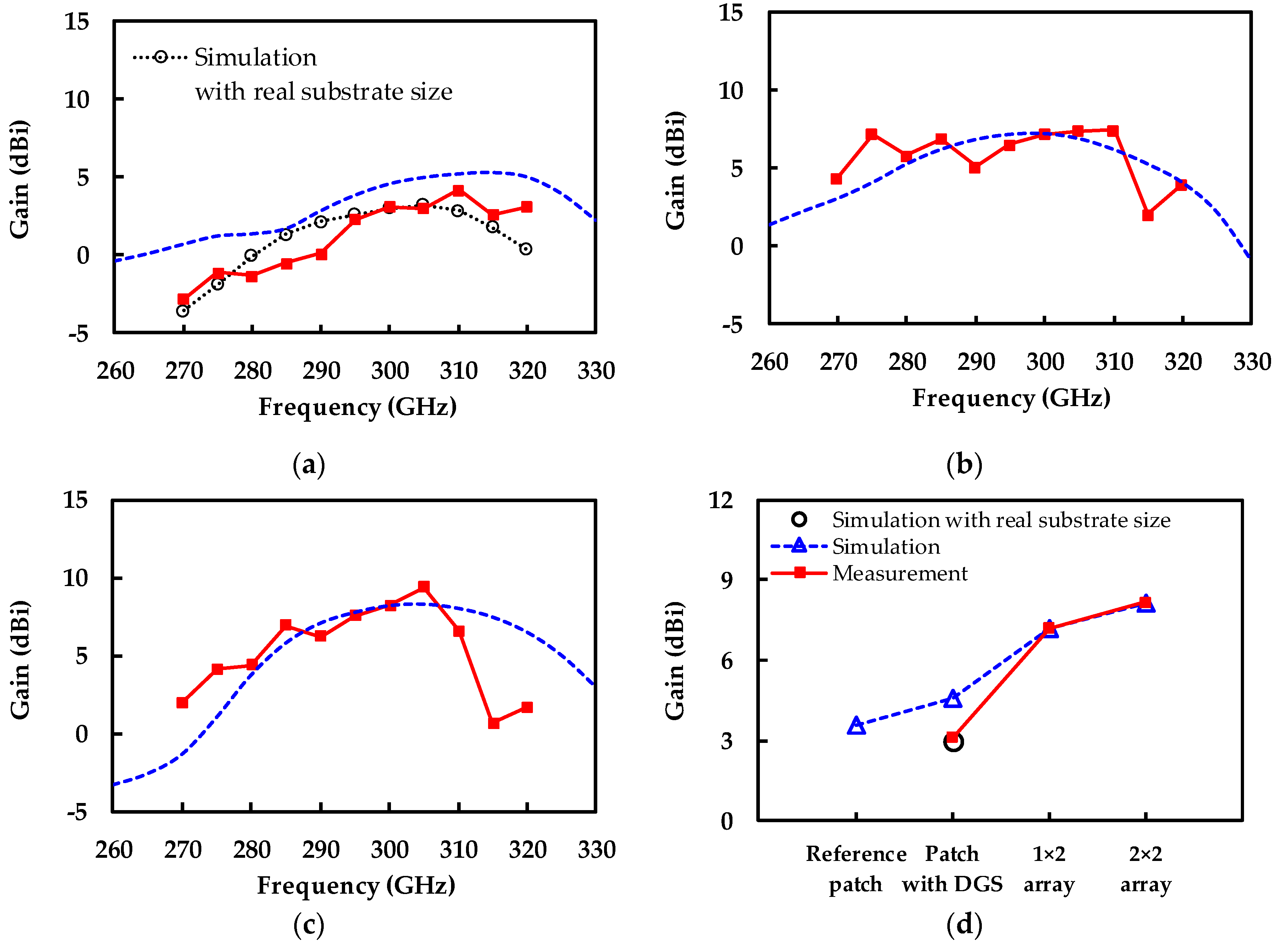
Figure 10 shows the measured reflection coefficient with the simulation results. The inserted 50 Ω line and RF pad are included in this simulation. Each antenna exhibits a broad bandwidth of 14.0% (antenna element), 21.3% (1 × 2 array), and 28.0% (2 × 2 array) at 300 GHz band. There exists some discrepancy between the measured and simulated reflection coefficients. One of the causes seems to be the uncertain location of the probe tips in the RF pads during on-wafer measurements.

3.2. Antenna Gain

The radiation characteristics of the fabricated on-chip antenna were measured using the in-house antenna measurement setup designed by the authors [11]. RF power is applied to the on-chip antenna under test (AUT) through the RF probe, and the radiated power is measured by the standard horn antenna and zero-biased detector which are installed on the spherical arm of the setup. The receive angle of the horn antenna can be manually controlled to measure the radiation pattern. The antenna gain of the AUT G A U T is determined by comparing the received power P r , A U T with the AUT connected, with the received power P r , h o r n with the AUT replaced with the standard horn antenna of a known gain G h o r n as follows [11,13,17].
G A U T = P r , A U T P r , h o r n + G h o r n + L p r o b e ,
where the probe loss ( L p r o b e ) is included in the calculation.
Figure 11a–c shows the measured gain with frequency of the antenna element, 1 × 2 array, and 2 × 2 array, respectively. Note that the measurement results include the loss by the RF pad and ~300 μm-long line of which loss is predicted to be approximately 0.7 dB at 300 GHz by the simulation. The gain of each antenna at 300 GHz is compared in Figure 11d. The antenna element, 1 × 2 array, and 2 × 2 array exhibit the measured gain of 3.1 dBi, 7.2 dBi, and 8.2 dBi, respectively, at 300 GHz. It clearly shows that the antenna gain increases with array size. However, the gain is increased by only 1.0 dB from 1 × 2 array to 2 × 2 array. This is because of on-chip feedline loss as expected from the simulation. The very long (650 μm in Figure 9c) connecting RF pad with 2 × 2 array also contributes to the gain drop. Therefore, the loss by the feedline structure limits the array size of the THz on-chip antenna array.
We can see the relatively large gain difference (~1.5 dB) between the simulation and measurement of antenna element in Figure 11a. It was found that the substrate size used in the simulation can affect the antenna gain. The previous simulations were performed for a small silicon substrate size of 0.9 mm × 1.4 mm to reduce the simulation time. However, it cannot predict well the substrate mode propagation along the silicon substrate. Figure 12a shows the real location of the antenna element in 4.0 mm × 4.0 mm silicon substrate. The simulated gain in this configuration is a few dB lower than that in the previous simulation using a small substrate. This simulation result is inserted in Figure 11a,d with a legend, “simulation with real substrate size”. It shows very good agreement with the measurement. Figure 12b shows the electric field distribution at 300 GHz in which we can see the electric field leak through the DGS of the antenna and propagate along silicon substrate, leading to additional loss and reduced gain. Interestingly, this substrate mode was greatly reduced in the antenna array. It is because antenna elements are placed about λ/2 apart in the array, so that the leakage waves cancel out each other and do not propagate through the substrate.

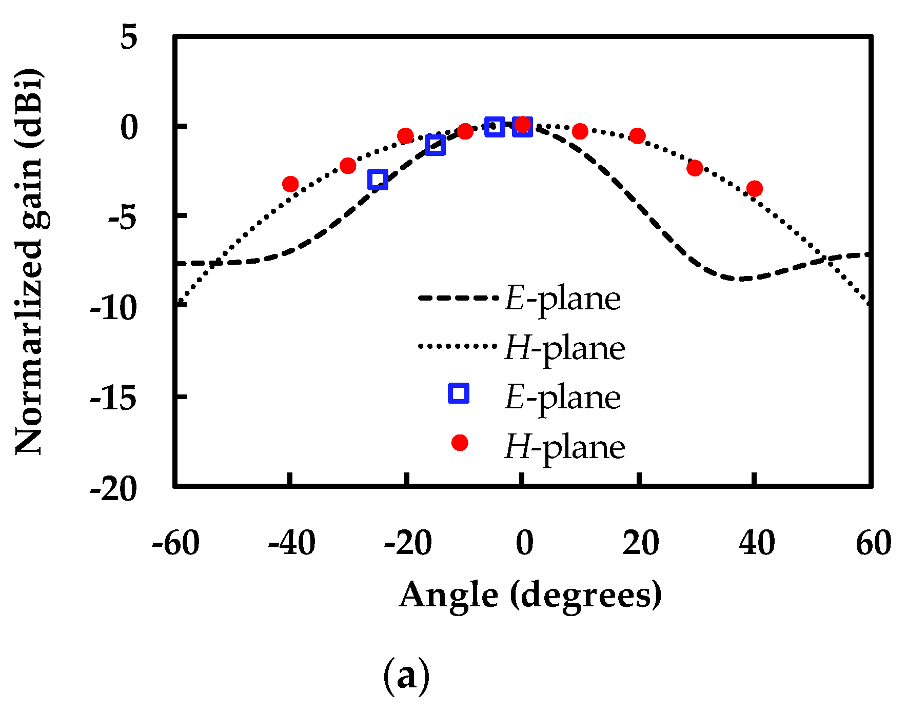
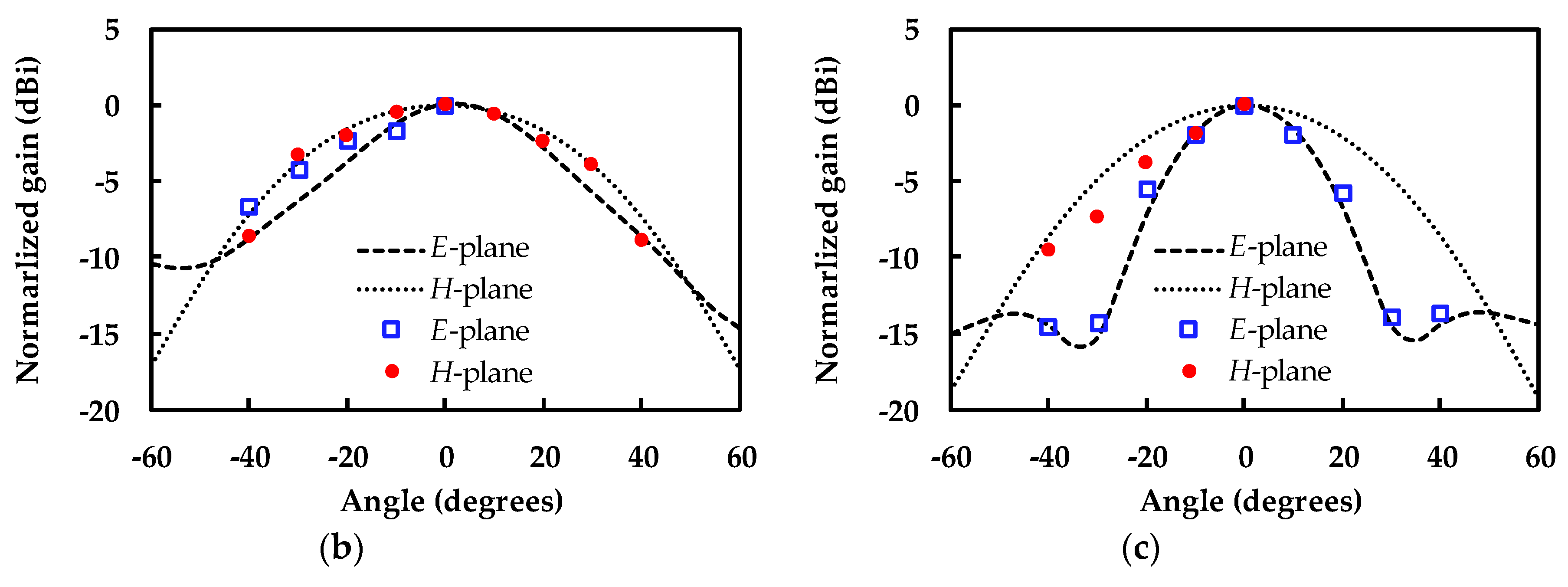
3.3. Radiation Pattern

Figure 13 shows the measured and simulated E-plane and H-plane radiation patterns at 300 GHz. The radiation patterns are well-predicted by the simulations. The beam width gets smaller as the array size increases, implying the increasing directivity [13]. The 2 × 2 array shows the measured 3 dB beam width of 26° and 16° in E- and H-planes, respectively. Cross-polarization radiations could not be measured due to the limitation of the antenna measurement setup, but the simulation shows that they are suppressed by at least 25 dB in the broadside direction for both the E- and H-planes of each antenna.

4. Conclusions

In this work, we designed the wideband and high gain CMOS on-chip patch antenna at 300 GHz and utilized it to the 1 × 2 and 2 × 2 antenna array to further increase antenna gain. Table 2 compares the performance of the reported CMOS on-chip antennas operating around 300 GHz. In order to achieve high gain, most antennas in this table utilized the additional process such as dielectric resonators, silicon lens, and LBE technique, which increases the overall antenna size and fabrication cost. On the contrary, we proposed the DGS antenna in a conventional CMOS process which can increase the isolation between antenna elements in the on-chip array, allowing high gain and high radiation efficiency within the compact size. The fabricated 2 × 2 antenna array shows a high gain of 8.2 dBi with a bandwidth of 28.0%. Therefore, the array designed in this work can be applied for the highly integrated on-chip array for THz wireless communications and radar sensors.

Author Contributions

Conceptualization, C.L. and J.J.; Methodology, C.L. and J.J.; Software, C.L.; Validation, C.L. and J.J.; Formal Analysis, C.L. and J.J.; Data Curation, C.L.; Writing–Original Draft Preparation, J.J.; Writing–Review and Editing, C.L. and J.J.; Visualization, C.L.; Supervision, J.J.; Funding Acquisition, J.J. All authors have read and agreed to the published version of the manuscript.

Funding

This work was partly supported by the Institute for Information & Communications Technology Planning & Evaluation (IITP) grant, funded by the Korean government (MSIT) (No. 2016-0-00185, Development of ultra-wideband terahertz CW spectroscopic imaging systems based on electronic devices). This work was also partly supported by a grant to the Terahertz Electronic Device Research Laboratory, funded by Defense Acquisition Program Administration and by the Agency for Defense Development (UD180025RD).

Conflicts of Interest

The authors declare no conflict of interest.

References

  1. Marchese, L.E.; Terroux, M.; Bolduc, M.; Cantin, M.; Desnoyers, N.; Bergeron, A. A 0.1 megapixel THz camera with 17-degree field of view for large area single shot imaging. In Proceedings of the 2014 39th International Conference on Infrared, Millimeter, and Terahertz waves (IRMMW-THz), Tuicson, AZ, USA, 14–19 September 2014; pp. 1–2. [Google Scholar] [CrossRef]
  2. Kašalynas, I.; Venckevičius, R.; Minkevičius, L.; Wahaia, F.; Janonis, V.; Tamošiônas, V.; Valušis, D.; Valušis, G.; Sešek, A.; Trontelj, J.; et al. High spatial resolution terahertz imaging of carcinoma tissues at 0.6 THz frequencies. In Proceedings of the 2016 41st International Conference on Infrared, Millimeter, and Terahertz Waves (IRMMW-THz), Copenhagen, Denmark, 25–30 September 2016; pp. 1–2. [Google Scholar] [CrossRef]
  3. Seok, E.; Shim, D.; Mao, C.; Han, R.; Sankaran, S.; Cao, C.; Knap, W. Progress and Challenges Towards Terahertz CMOS Integrated Circuits. IEEE J. Solid-State Circuits 2010, 45, 1554–1564. [Google Scholar] [CrossRef]
  4. Hu, S.; Xiong, Y.Z.; Zhang, B.; Wang, L.; Lim, T.G.; Je, M.; Madihian, M. A SiGe BiCMOS Transmitter/Receiver Chipset With On-Chip SIW Antennas for Terahertz Applications. IEEE J. Solid-State Circuits 2012, 47, 2654–2664. [Google Scholar] [CrossRef]
  5. Sherry, H.; Hadi, R.A.; Grzyb, J.; Öjefors, E.; Chthelina, A.; Kaiser, A.; Pfeiffer, U.R. Lens-integrated THz imaging arrays in 65-nm CMOS technologies. In Proceedings of the IEEE Radio Frequency Integrated Circuits Symposium (RFIC), Baltimore, MD, USA, 5–7 June 2011; pp. 365–368. [Google Scholar] [CrossRef]
  6. Grzyb, J.; Zhao, Y.; Pfeiffer, U.R. A 288-GHz Lens-Integrated Balanced Triple-Push Source in a 65-nm CMOS Technology. IEEE J. Solid-State Circuits 2013, 48, 1751–1761. [Google Scholar] [CrossRef]
  7. Babakhani, A.; Rutledge, D.B.; Hajimiri, A. mm-wave phased arrays in silicon with integrated antennas. In Proceedings of the IEEE Antennas Propag. Int. Symp., Honolulu, HI, USA, 9–15 June 2007; pp. 4369–4372. [Google Scholar] [CrossRef] [Green Version]
  8. Schmalz, K.; Borngraber, J.; Debski, W.; Elkhouly, M.; Wang, R.; Neumaier, P.F.; Kissinger, D.; Hubers, H. 245-GHz Transmitter Array in SiGe BiCMOS for Gas Spectroscopy. IEEE Trans. Terahertz Sci. Technol. 2016, 6, 318–327. [Google Scholar] [CrossRef]
  9. Tajima, T.; Song, H.J.; Yaita, M. Compact THz LTCC Receiver Module for 300 GHz Wireless Communications. IEEE Microw. Wirel. Compon. Lett. 2016, 26, 291–293. [Google Scholar] [CrossRef]
  10. Deng, X.D.; Li, Y.; Liu, C.; Wu, W.; Xiong, Y.Z. 340 GHz On-Chip 3-D Antenna With 10 dBi Gain and 80% Radiation Efficiency. IEEE Trans. Terahertz Sci. Technol. 2015, 5, 619–627. [Google Scholar] [CrossRef]
  11. Kim, H.; Choe, W.; Jeong, J. A Terahertz CMOS V-Shaped Patch Antennas with Defected Ground Structure. Sensors 2018, 18, 2432. [Google Scholar] [CrossRef] [PubMed] [Green Version]
  12. Han, R.; Afshari, E. A CMOS High-Power Broadband 260-GHz Radiator Array for Spectroscopy. IEEE J. Solid-State Circuits 2013, 48, 3090–3104. [Google Scholar] [CrossRef]
  13. Balanis, C.A. Antenna Theory: Analysis and Design, 4th ed.; Wiley: New York, NY, USA, 2016. [Google Scholar]
  14. Pozar, D.M. Surface wave effects for millimeter wave printed antennas. In Proceedings of the 1983 Antennas and Propagation Society Int. Symp., Houston, TX, USA, 23–26 May 1983; pp. 692–695. [Google Scholar] [CrossRef]
  15. Yoon, S.J.; Choi, J. A Low-Profile Broadband Array Antenna for Home Repeater Applications. J. Electromagn. Eng. Sci. 2018, 18, 261–266. [Google Scholar] [CrossRef]
  16. Kothapudi, V.K.; Kumar, V. SFCFOS Uniform and Chebyshev Amplitude Distribution Linear Array Antenna for K-Band Applications. J. Electromagn. Eng. Sci. 2019, 19, 64–70. [Google Scholar] [CrossRef]
  17. Kang, J.S.; Kim, J.H.; Park, J.I. Comparison of antennas parameters of R-/S-band standard gain antennas. In Proceedings of the 2015 International Workshop on Antenna Technology (iWAT), Seoul, Korea, 4–6 March 2015; pp. 369–371. [Google Scholar] [CrossRef]
  18. Li, C.H.; Chiu, T.Y. 340-GHz Low-Cost and High-Gain On-Chip Higher Order Mode Dielectric Resonator Antenna for THz Applications. IEEE Trans. Terahertz Sci. Technol. 2017, 7, 284–294. [Google Scholar] [CrossRef]
Figure 1. (a) Back-end-of-line (BEOL) structure of 65 nm CMOS process and (b) reference patch antenna.
Electronics 09 01137 g001
Figure 2. Proposed patch antenna with defected ground structure (DGS).
Electronics 09 01137 g002
Figure 3. Simulation of 1 × 2 antenna array using (a) reference antenna element (Figure 1b) and (b) using proposed antenna with DGS (Figure 2).
Electronics 09 01137 g003
Figure 4. Simulated results of (a) coupling and (b) radiation efficiency at 300 GHz (squared: without DGS, triangle: with DGS).
Electronics 09 01137 g004
Figure 5. Simulated performance of 1 × 2 antenna array using the proposed patch with DGS at 300 GHz as a function of element spacing. (a) The 1 × 2 antenna array with termination impedance of 25 Ω. (b) Gain and directivity. (c) Radiation efficiency.
Electronics 09 01137 g005
Figure 6. Design of feedlines of 1 × 2 antenna array. (a) Schematic. (b) Simulated reflection coefficient depending on characteristic impedance of feedline (Z0,TL2).
Electronics 09 01137 g006
Figure 7. (a) Designed 2 × 2 antenna array. (b) Feedline structure of 2 × 2 antenna array.
Electronics 09 01137 g007
Figure 8. Comparison of simulated performance of designed antenna. (a) Bandwidth for reflection coefficient less than −10 dB. (b) Gain and directivity. (c) Radiation efficiency.
Electronics 09 01137 g008
Figure 9. Photographs of fabricated on-chip antenna in a 65 nm CMOS process. (a) Antenna element. (b) The 1 × 2 antenna array. (c) The 2 × 2 antenna array.
Electronics 09 01137 g009
Figure 10. Measured and simulated reflection coefficients of fabricated on-chip antenna (dashed: simulation, squared: measurement). (a) Antenna element. (b) The 1 × 2 antenna array. (c) The 2 × 2 antenna array.
Electronics 09 01137 g010
Figure 11. Measured and simulated gain of fabricated on-chip antenna (dashed: simulation, solid with squares: measurement). (a) Antenna element. (b) The 1 × 2 antenna array. (c) The 2 × 2 antenna array. (d) Gain comparison.
Electronics 09 01137 g011
Figure 12. Simulation of antenna element in real substrate size. (a) Antenna in 4.0 mm × 4.0 mm silicon substrate. (b) Electric field distribution at 300 GHz.
Electronics 09 01137 g012
Figure 13. Simulation and measurement of radiation patterns at 300 GHz (lines: simulation, symbols: measurement). (a) Antenna element. (b) The 1 × 2 antenna array. (c) The 2 × 2 antenna array.
Electronics 09 01137 g013aElectronics 09 01137 g013b
Table 1. Dimensions of designed patch antenna with DGS at 300 GHz (in μm).
WpLpWPRLPRGPRWDGSLDGSGDGSGM
250200601801090852060
Table 2. Comparison of the reported THz CMOS on-chip antenna.
ReferenceAntenna TypeProcessFrequency
(GHz)
Bandwidth
(%)
Gain
(dBi)
Size
(mm2)
Additional
Process
[6]Dipole (single)65 nm CMOS288n.a.18.3 *0.29 × 0.29Lens
[8]Dipole (1 × 4 array)180 nm BiCMOS24516.3 *11.0 **3.7 × 5.4(with IC)LBE 1
[12]Patch (single)130 nm CMOS340n.a.3.3 *n.a.none
12.010.00.8 × 0.9DR 2
[18]Patch (single)180 nm CMOS3417.0 *7.9 *0.4 × 0.3DR
This workPatch (element)65 nm CMOS30014.03.10.23 × 0.42none
Patch (1 × 2 array)21.37.20.30 × 0.92
Patch ( 2× 2 array)28.08.20.92 × 0.79
* Simulation result; ** Calculated from measurement; 1 LBE: localized backside etch; 2 DR: dielectric resonator.

