Article

Simplified Modal-Cancellation Approach for Substrate-Integrated-Waveguide Narrow-Band Filter Design

1
Computer, Electrical and Mathematical Science and Engineering (CEMSE) Division, King Abdullah University of Science and Technology (KAUST), Thuwal 23955-6900, Saudi Arabia
2
Department of Electrical and Electronics Engineering, University of Jeddah, Jeddah 21589, Saudi Arabia
*
Author to whom correspondence should be addressed.
Electronics 2020, 9(6), 962; https://doi.org/10.3390/electronics9060962
Submission received: 18 May 2020 / Revised: 2 June 2020 / Accepted: 6 June 2020 / Published: 9 June 2020

Abstract

:
Current substrate-integrated-waveguide (SIW) filter design methodologies can be extremely computational and time-inefficient when a narrow-band filter is required. A new approach to designing compact, highly selective narrow-band filters based on smartly positioned obstacles is thus presented here. The proposed modal-cancellation approach is achieved by translating or eliminating undesired modes within the frequency of interest. This is performed by introducing smartly located obstacles in the maxima and nulls of the modes of interest. This approach is different from the traditional inverter technique, where a periodic number of inductive irises are coupled in a ladder configuration to implement the desired response of an nth-order filter, and significantly reduces the complexity of the resulting filter structure. Indeed, the proposed method may be used to design different filters for several frequency bands and various applications. The methodology was experimentally verified through fabricated prototypes.

1. Introduction

The increasing need for higher bandwidth in communication networks calls for systems that can support many frequency bands [1]. For example, modern smartphone networks have continued adding frequency bands to the point where 30 bands are not uncommon [2]. Such networks/systems use filters operating at radio-frequency (RF), microwaves and millimeter-wave parts of the spectrum to select or reject various frequency channels [1]. Rectangular cavities are often used as filters in satellite communication, where low insertion loss and high-power handling capability are required [3,4]. However, filters that rely on rectangular waveguides are large and heavy, which has limited their widespread use in other communication networks. As an alternative, substrate-integrated waveguides (SIWs) have gained popularity due to their high quality, compact size, and power efficiency. Their planar structure allows for easy integration that may lead to full on-chip RF– complementary-metaoxide-semiconductor (CMOS) systems, reducing the amount of material and space needed for electronics. An SIW consists of metal via holes embedded in a planar dielectric structure between two metal layers. Such a structure can be manufactured using standard fabrication processes such as printed-circuit-board (PCB) manufacturing, low-temperature cofired ceramics (LTCC), and nanofabrication processes in the case of a silicon substrate [5,6,7]. The resulting device can be easily connected to planar circuits such as microstrip lines and coplanar waveguides (CPW) [8], allowing for the straightforward integration on active circuits.
Traditional filter-design methods, under the assumption of periodicity in the structure, exploit the mapping between network elements and the structure’s unit-cell parameters [9,10]. Among these design methods, the K-inverter scheme has dominated the way in which SIW bandpass filters are designed [7,11,12,13]. For a bandpass K-inverter filter, ladder-configuration metallic irises are used as the LC components of the desired nth-order filter. Once the normalized impedances of the inverters are found, the physical dimensions of the corresponding iris are obtained. Multiple attempts were previously made to simplify the filter-design process, with space mapping being preferred due to its computational and theoretical approaches [14].
Sensing applications, modulation schemes, and a full electromagnetic spectrum require narrow-band filters. Most filter-design methodologies operate conveniently when a broadband filter is required; however, they can result in a complex process for the design of a highly selective filter. In this work, we propose a fast and simple method that intelligently selects transverse-electric (TE) modes to efficiently obtain a narrow-filter response at any desired frequency. Each mode has a set of nulls and maxima inside the SIW. The nulls and maxima for the TE electric modes can be effectively disturbed by the presence of obstacles that can tailor electromagnetic behavior into a desired application [15]. By introducing a limited number of metallic-via holes at the maximal-electric-field locations of the undesired modes and in the nulls of the desired ones, a highly selective narrow-band behavior can be obtained. Using a full-wave simulator, the SIW is discretized into square cells that tell the information of the electric field at the frequency of interest. As the electric modes for each frequency of interest are simulated and extracted, the obstacles can be precisely collocated to give extremely high selectivity. Once an obstacle is added, the SIW is again discretized to define the optimal positions for future obstacles if needed. This approach is fast and efficient if a low-complexity high-quality factor and low-order filters are required.
The remainder of the paper is organized as follows. Section 2 refers to the mode-cancellation technique using smartly placed optimized obstacles. Section 3.1 shows different examples of SIW filters, while Section 3.2 illustrates the experiment results of a primary filter made in FR4 epoxy with an inductive obstacle at its center. Lastly, Section 4 provides some concluding remarks.

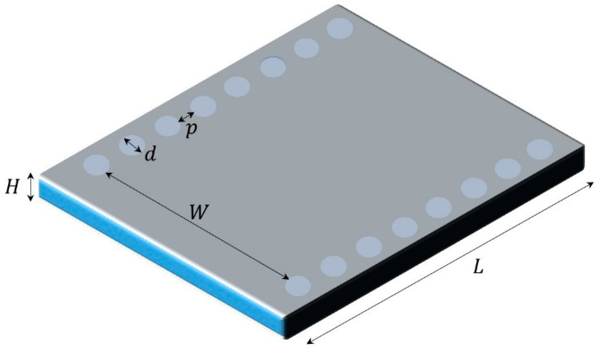
2. Materials and Methods

This section describes the implementation model of the proposed narrow-band SIW filter-design methodology.

2.1. Mode Selection

The SIW structure is shown in Figure 1. It consists of top and bottom metal plates with a dielectric substrate in-between. Two parallel rows of metal vias that shortcut both metal layers are located at the edges of the structure. The vias must be shorted to both metal plates to provide vertical current paths. The frequencies of the waveguide modes are given by [16]
f c = c 2 π ϵ r ( m π L ) 2 + ( n π W ) 2 ,
where the effective parameters are assumed (these are air-filled rectangular waveguide width W , length L , thickness H , and dielectric permittivity ϵ r effectively reduced to a dielectric-filled SIW). Additionally, two conditions are required for the distance between the centers of the vias (pitch) and their diameter to allow wave propagation (higher dimensions result in high power leakage) [17]:
d < λ g 5 ,   and   p < 2 d .
An optimization process is performed several times to match the fence-via radius with the obstacle-via radius. If a microstrip-to-SIW transition is required, one can refer to Appendix A (propagating frequencies may be shifted by the transition introduction).
Since the vertical metal walls of the rectangular waveguides are replaced by rows of vias or via fences for the SIW structures, the modes of both structures are close to each other. Since the fence vias resemble a metallic wall, transverse-magnetic (TM) modes do not propagate. On the basis of multiple-mode response, one can smartly locate obstacles that attenuate all modes except for a desired one. The SIW smart-dimension selection starts with substrate selection (having characteristics ϵ r and δ ). Afterwards, the thickness of the substrate is carefully chosen; an extremely thin structure has high conduction losses and low power capabilities [18]. Mode T E m , n is selected to propagate at f c with fixed width W and length L that controls the frequency of operation.
Mode T E 1 , 0 is usually avoided due to its easy cancellation by any obstacle. Operating under a second mode, T E 2 , 0 , is usually preferred due to the simplicity of canceling the first- and higher-order modes by locating an obstacle in the center of the SIW. The quality factor of the filter can be enhanced using modal recombination; for this, immediately higher-order mode T E m + , n +   ( m + and n + are the values of m and n for this mode) is chosen to propagate closely to f c at f c + (immediately lower-order mode T E m , n can be used as well). In this case, after fixing W , L must simultaneously solve the previous equation and
c 2 π ϵ r ( m + π L ) + ( n + π W ) 2 f c + = 0 .
If a wider band is required, the location can be slightly upshifted. For efficient miniaturization, the diameter of the vias is selected as d = λ g / 40 and pitch distance as p = 2 d / 8 ; this guarantees a compact metallic-via fence.

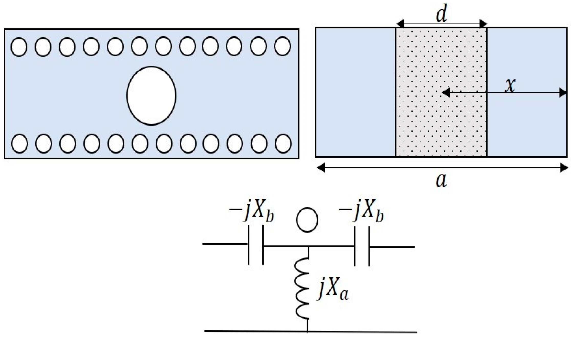
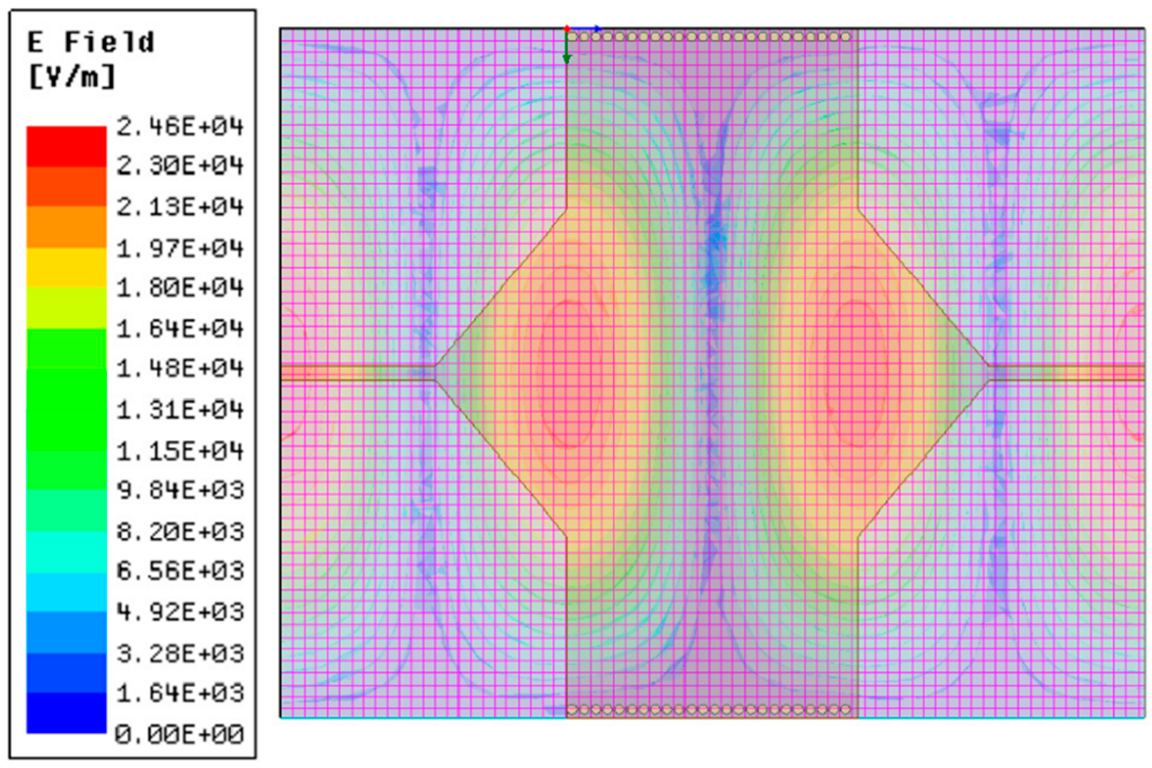
2.2. Mode Cancellation Using Inductive Obstacles

Equivalent wavelength formulations that apply for an inductive obstacle inside a dielectric-filled SIW (value of a is equal to W from Figure 1 when vias are centered) are
λ = c ϵ r f c ,
λ g = λ 1 ( λ 2 a ) 2 .
Metallic-via obstacles of a circular cross-section (Figure 2) with an axis parallel to the electric field are modeled as four-terminal resonant (LC) impedance blocks, as stated in [19]
X a Z 0 X b 2 Z 0 = a 2 λ g csc 2 ( π x a ) [ S 0 ( π d 2 λ ) 2 ( π d 2 a ) 2 ( S 0 cot ( π x a ) S 1 ) 2 ] ,
X b Z 0 a λ g   ( π d a ) 2 1 + 11 24 ( π d a ) 2 ,  
where j X b is the reactance for the capacitors, and j X a is the equivalent reactance of the inductance. These reactances are conditioned to
S 0 = ln ( 4 a π d ) 2 + 2   n = 3 , 5 [ 1 n 2 ( 2 a λ ) 2 1 n ] ,
S 2 = ln ( 4 a π d ) 5 2 + 11 3 ( λ a ) 2 ( λ a ) 2 n = 3 , 5 [ n 2 ( 2 a λ ) 2 n + 2 n ( a λ ) 2 ] .
There are two variables of control for the introduced equivalent impedance, radius and position. To simplify filter fabrication, the radius can be fixed to the same one used for the metallic fences. Capacitance j X b is fixed, leaving x as the only variable of control for inductance j X a . After defining the obstacle and evaluating the dimensions for the desired T E modes, SIW discretization may start. The SIW is then discretized into square cells C i , j with a side of d + p , as shown in Figure 3a.
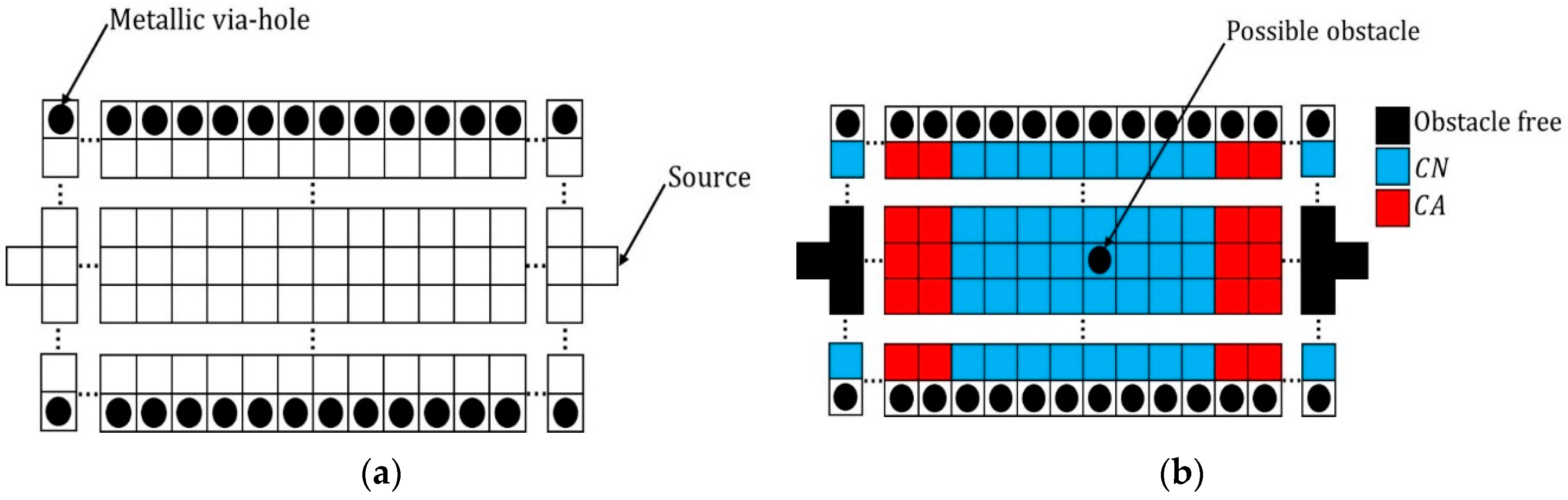
Algorithm 1 Defining frequency-selective obstacles.
Electronics 09 00962 i001
For the desired T E m , n , the electric field is obtained for each C i , j cell; each of them is identified in a binary way as
C i , j = { C A   electric   mode , C N   electric   field   null .  
In Figure 3b, a third kind of cell is highlighted in black as obstacle-free regions; this is due to the high impedance so close to the source, and that may easily forbid propagation. The role of the obstacles is to act as resonators that couple the energy of only the selected frequencies. A frequency sweep between f c f c / 4 f f c + f c / 4 is then realized after modeling the empty SIW in Ansys HFSS; afterwards, the electric-mode peak frequencies are identified. Frequencies for the neighbor modes of T E m , n are then used as solving frequencies in the simulator. The electric fields inside the SIW are then exported, discretized, and classified as C A and C N . Assuming that T E + is the immediate-neighbor higher mode and T E the immediate-neighbor lower mode for TE, common C i , j cells are compared to obtain C i , j cells that might include obstacle
C i , j = { 1   i f   C A i , j + = C A i , j = C N i , j , 0   i f   C A i , j + = C A i , j = C A i , j .
Subsequently, maximal number of vias max ( v ) is selected as the maximal number of obstacles. The obstacles are positioned as individual metallic vias or as compound windows. Because the search area can be extensively high compared to max ( v ) , we reduced the search domain into the closest nulls near the maxima of interests. The introduced impedance was validated using the LC models for the vias and their position inside the SIW; the distance between components was modeled as transmission lines. Depending on the obstacle array, cavity resonators can be introduced to the SIW. The vias were modeled in Ansys HFSS, and modal cancellation was verified; if the requirements were not satisfied, the number of vias could be increased, or the radius of the existing ones could be altered. Optimetric, a tool from HFSS, can simplify this optimization process. The extraction of the electric field inside the SIW is not straightforward using Ansys HFSS. After a solution is obtained, a nonmodel object must be created; in this case, polylines that represented the desired cells. Each cell was made up of four intersections, each of them giving an electric field; the average electric field was calculated. It was not necessary to discretize the whole design, but just the main areas of interest (nulls and maxima). The summary of the design procedure is stated in Algorithm 1.

3. Results

This section describes the implementation of the previously described algorithms in filter designs for different frequency bands. It finalizes with a fabricated proof of concept in which the dimensions of the filter were correctly optimized.

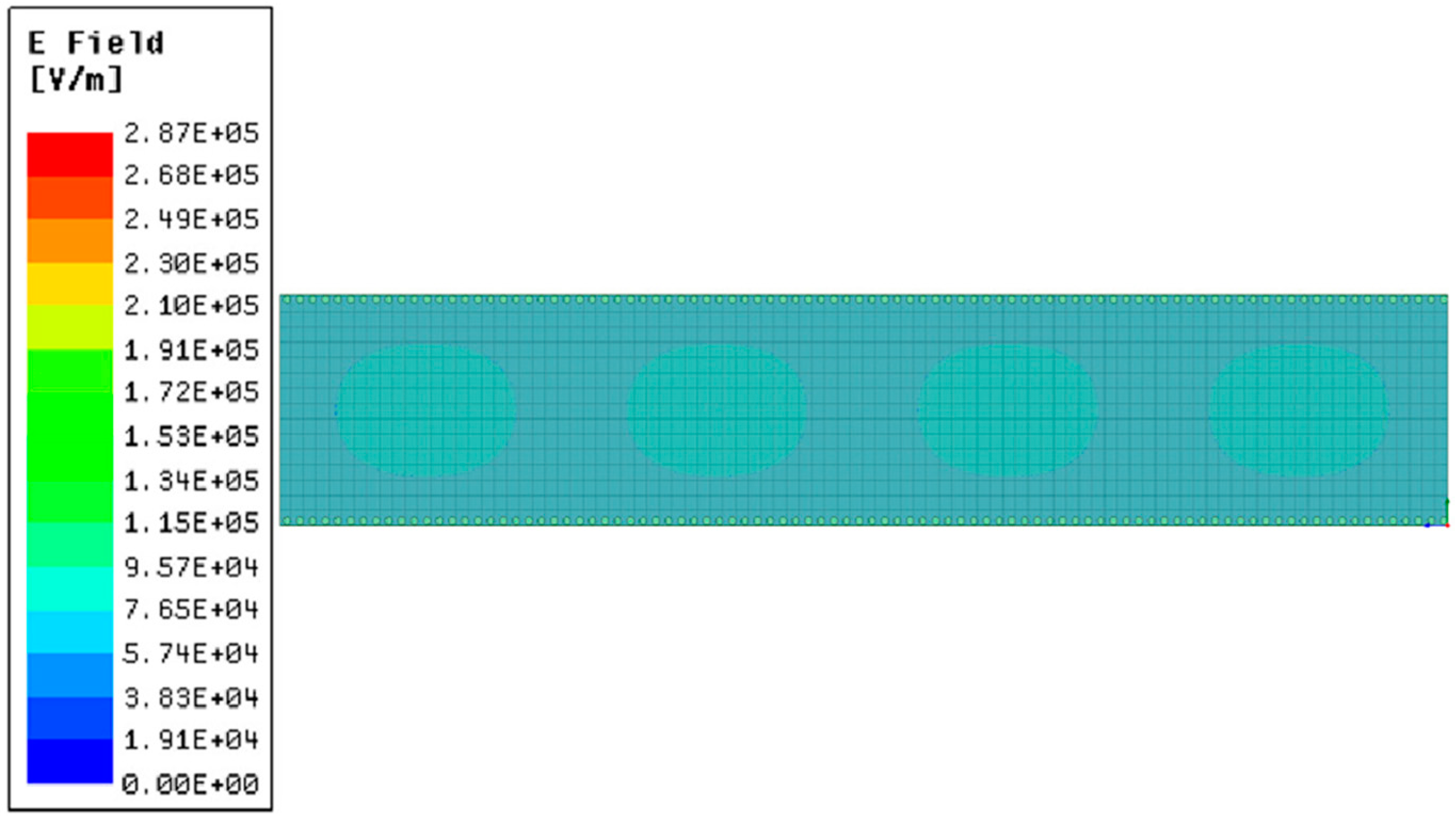
3.1. Narrow-Band Filter Design

Transmission and reflection parameters S 21 and S 11 were used to evaluate the performance of different filters at different frequency bands. The main advantage of this technique is its easy adaptability to any frequency band. The dimensions, structure, and operation of filters for various frequencies were studied according to the following objectives:
  • Multiple transverse electromagnetic modes should be tested.
  • Verify the effect of the microstrip–SIW transition for different modes. For the sake of simplicity, the first filter was modeled as a no tapered SIW–microstrip transition.
  • Different materials were tested using the proposed methodology. Complementary-metal-oxide-semiconductor (CMOS) integration requires the use of silicon (undoped silicon with ϵ r = 11.9 ) as the substrate of the SIW devices, while traditional radio-frequency (RF) circuitry uses common FR4 and Rogers substrates.
  • Devices with minimal sizes are always desired; for this, varying thicknesses of silicon were tested for different frequency ranges.
Several filters were designed according to the previous objectives. Three different frequency bands are proposed for validating the methodology through simulations: 28, 5.8, and 3.2 GHz. Silicon, traditional Rogers duroid®, and FR4 were used. Ansys HFSS was used with a PC setup with two processors, Intel Xeon Gold 6130 CPU @ 2.10 GHz and 128 GB of RAM. Each iteration consisted of running a simulation in Ansys in HFSS and then introducing its results into MATLAB, where the set of algorithms was executed. Each full-wave simulation took approximately 25 min to complete, while MATLAB identification could take a maximum of five minutes, thus adding to a total of 30 min per iteration. Each design could take approximately eight iterations to complete, leading to a total of 240 min of computational time per design. The lower-frequency filter was optimized to be fabricated in a simple manner by an LPKF s103 PCB maker.

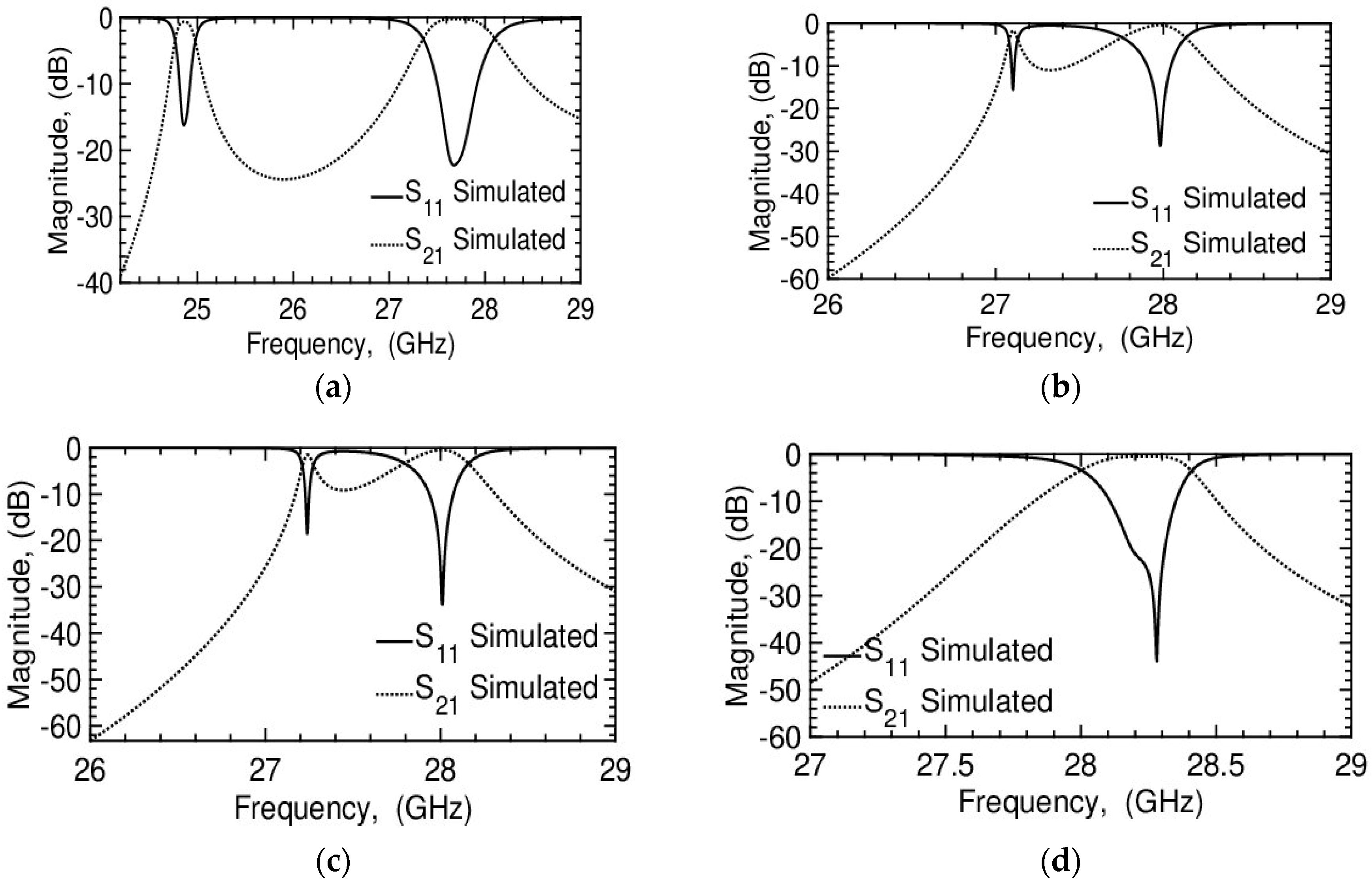
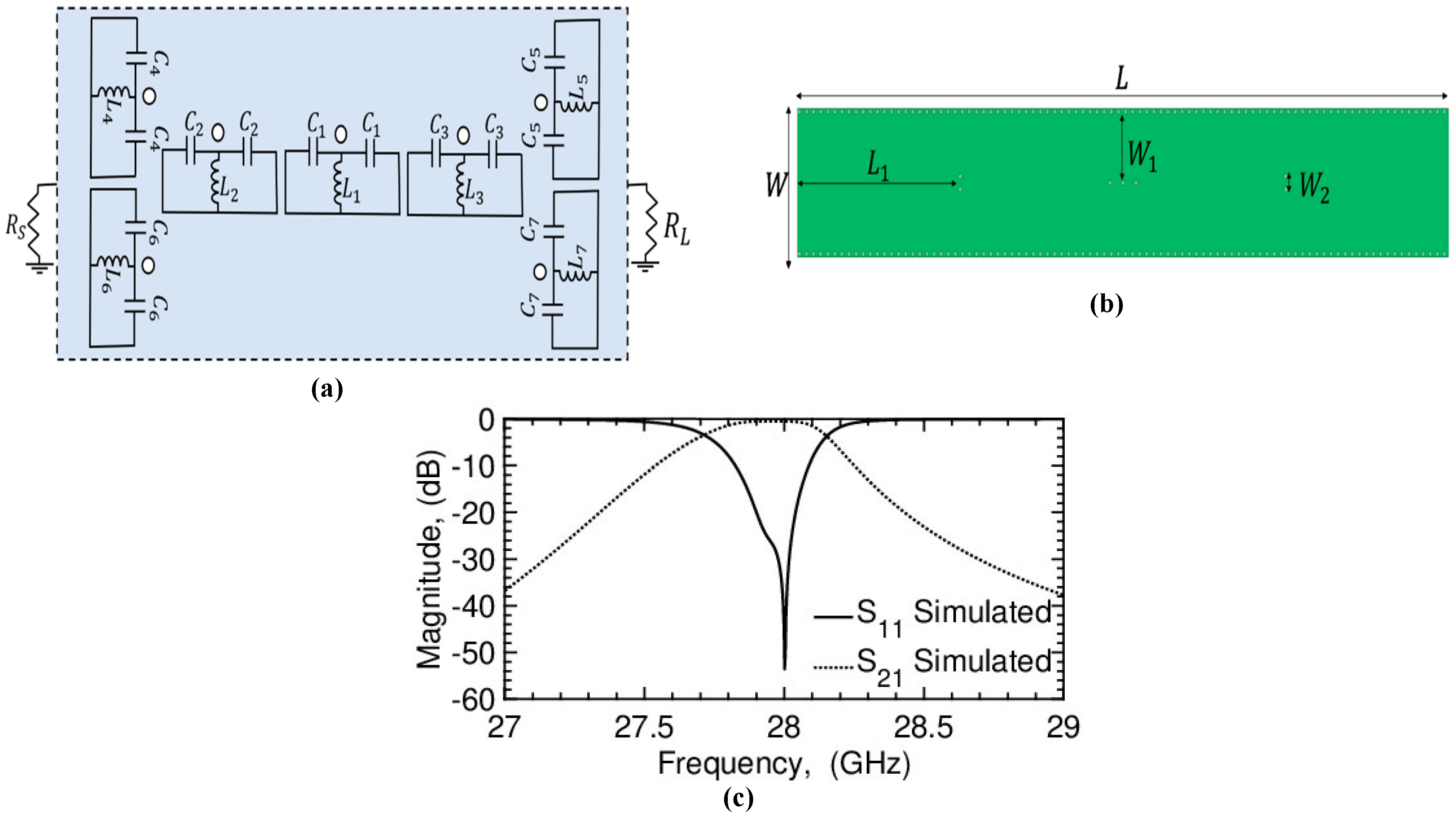
3.1.1. 28 GHz Filter Based on Smart Modal Selection

Millimeter-wave communication is a promising technological direction, as the spectrum is less crowded and higher bandwidth is available. The band around 28 GHz is expected to be massively used under 5G and 6G standards; it is of utmost necessity to design miniaturized filters for this range of frequencies using as few components as possible. A filter operating in the T E 4 , 1 mode was analyzed. Rogers 5880 duroid® with ϵ r = 2.2 , δ = 0.0004 , and 1.575 mm of thickness with two 18 µm layers of copper is used as the substrate. The filter consisted of a rectangular SIW ( W = 4.54 mm and L = 27.55 mm) with 0.16 mm vias in diameter and a pitch of 0.14 mm. Our mode of interest had its two closest neighbors at 26.24 GHz and 30.05 GHz. The SIW was discretized, as shown in Figure 4, for the three frequencies of interest. The C N cells of 0.3 mm size were exported from Ansys HFSS. Due to the electric-field configuration of the electric mode, seven inductive obstacles were selected as max ( v ) . After obtaining the null cells, we selected the geometric center of the SIW as the starting point. One obstacle with a diameter of 0.16 mm was positioned in the geometric. The immediate lower-order mode had a strong coupling inside the waveguide; as can be seen after the first obstacle introduction (Figure 5a), modal recombination was preferable.
The number of obstacles was increased, and the modal recombination can be seen in Figure 5. Lastly, seven equal vias 0.16 mm in diameter were located symmetrically inside the structure (equivalent impedance shown in Figure 6a). Three vias were located in the center null, while the four others were positioned vertically on the sides. Utilizing the circuit equations (Section 2.2), the MATLAB solver, and Optimetrics from HFSS, the filter was designed to have a narrow-band response with low insertion loss. To obtain the desired behavior, only seven iterations were needed to have a narrow response, that being much faster to converge than other computer-aided techniques [20,21]. The implementation of Algorithm 1 for this 28 GHz narrow-band filter is shown in Algorithm 2. Lastly, the geometry of Figure 6b was selected. The corresponding frequency response performed by HFSS is shown in Figure 6c. The filter had 20 dB matching in the frequency band of 27.90–28.04 GHz with a mean insertion loss of 0.4643 dB. The amount of copper used for the metal layers, and the metallization of the silver used to fill the vias strongly influenced the quality factor of the filter.
Algorithm 2: Application of Algorithm 1 on the design of 28 GHz narrow-band filter.
Electronics 09 00962 i002

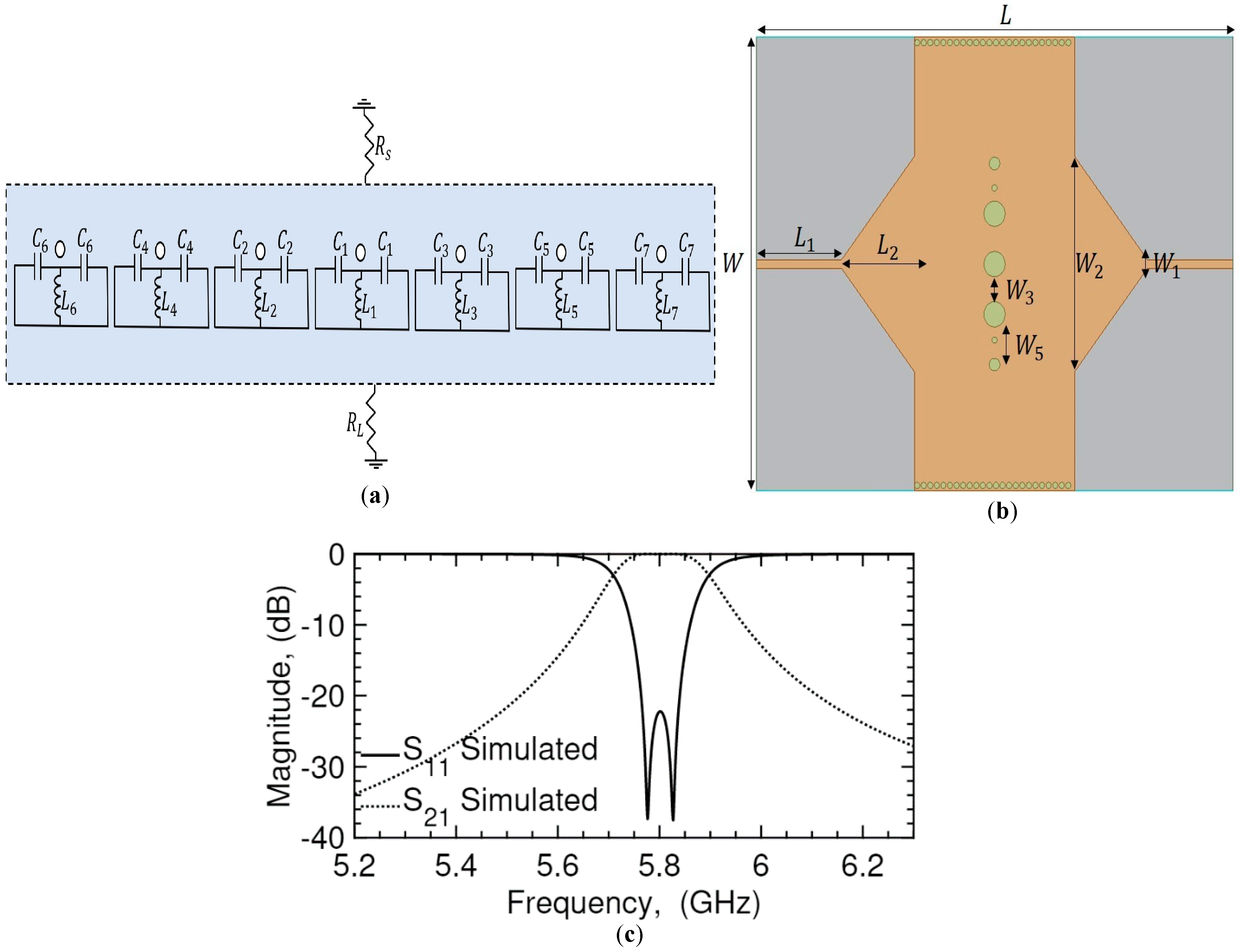
3.1.2. 5.8 GHz Filter Based on Smart Modal Selection

The sub-6 GHz band is currently one of the most relevant 5G frequency bands; miniaturized SIW topologies are required. Silicon is the primary substrate in existing electronics; having high dielectric permittivity, easier miniaturization is possible in contrast to low-permittivity duroid®. A silicon SIW filter based on T E 3 , 1 mode is proposed. The filter includes a tapered transition between the microstrip line and waveguide for smooth field matching. Typical thickness for silicon wafers (400 µm) with ϵ r = 11.9 is used as the substrate. Thinner silicon wafers would not allow propagation due to high conductivity losses [18]. The bottom and top metallic layers were assumed to be 1   µm thick. The diameter of the vias of the metal fence was 0.271 mm, with a pitch of 0.0678 mm between each. The layout of the proposed filter after discretization is shown in Figure 7 with the tapered transition.
The mode of interest had its closest neighbors at 4.19 GHz and 7.42 GHz. Again, max ( v ) was equal to 7. The electric-field configuration for the empty filter at 5.8 GHz showed maxima in the tapered transition. For 4.19 GHz, the maximum appeared in the center of the SIW; however, the electric mode around 7.42 GHz shared different maxima with 5.8 GHz. Modal recombination was mandatory. The only null area where vias could be embedded was in the center of the SIW; any other would attenuate the mode of interest. Eight iterations are necessary to reach proper modal recombination. The obstacles’ dimensions and positions were obtained using the equivalent impedance expressions with MATLAB, and then optimized using HFSS tool Optimetrics. Initially, a wide via of 0.542 mm radius was added at the center of the SIW, thus canceling the lower modes. Including two more vias, the higher mode was downshifted. Lastly, including two vias of 0.1355 mm radius and two of 0.271 mm radius allowed for appropriate modal recombination. The final filter had the equivalent filter in Figure 8a, and its dimensions are shown in Figure 8b. The structure consisted of an SIW–microstrip tapered transition with two cavity resonators constructed by the smart-obstacle position methodology. The filter had a 20 dB matching band of 5.76–5.84 GHz (Figure 8c) with a mean insertion loss of 0.02 dB.

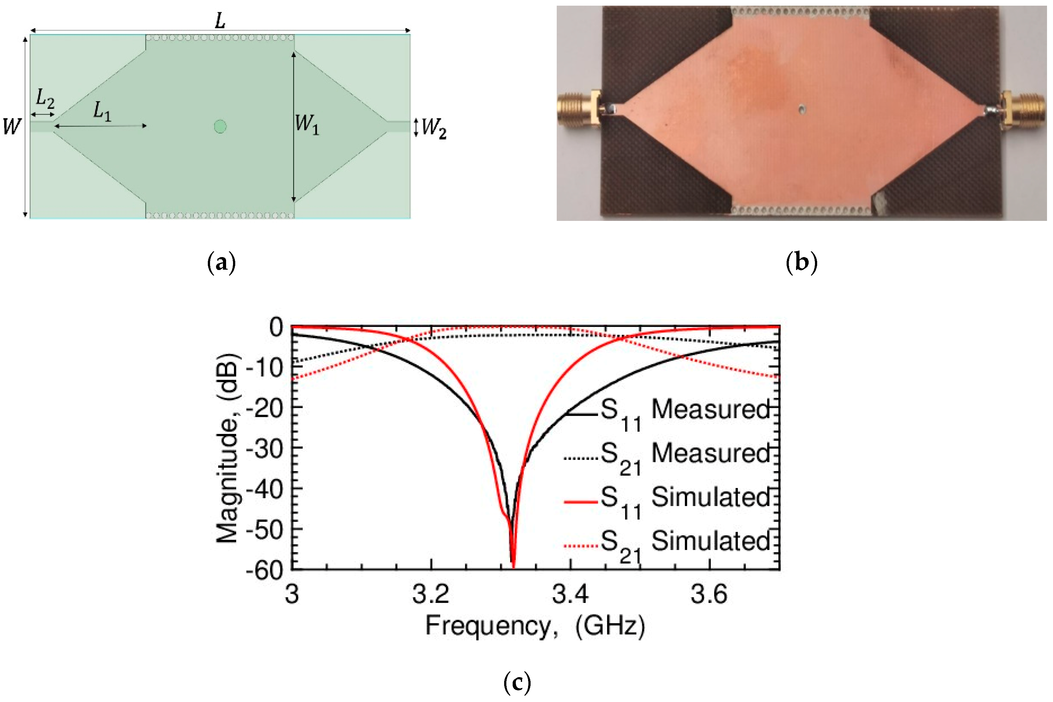
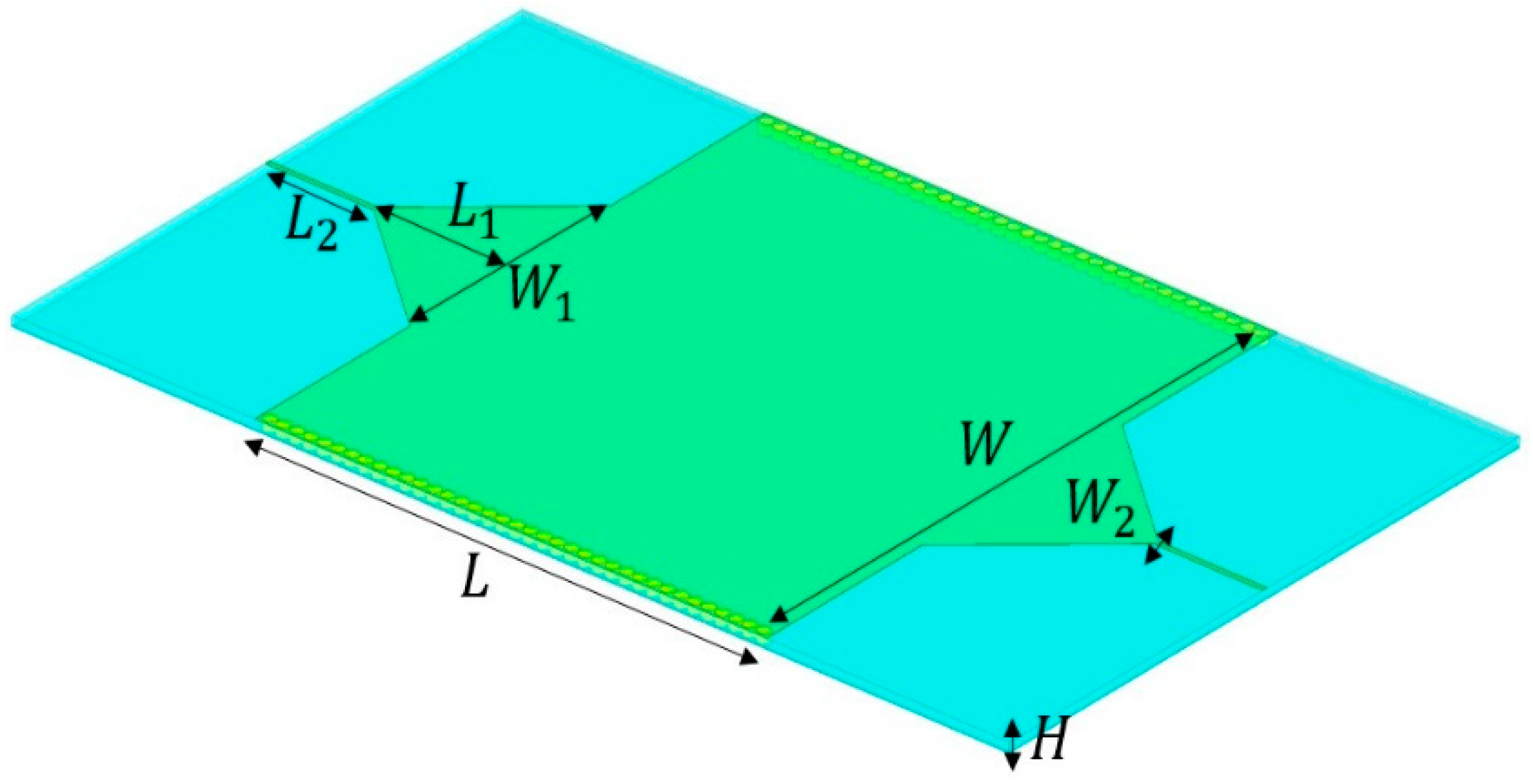
3.2. Fabrication and Proof of Concept for 3.2 GHz Filter

A low-frequency 3.2 GHz FR4 filter (having a copper layer of 18   µm and a loss tangent of δ = 0.002 ) was used to prove the efficiency of a smart selection of the obstacle and its position in the waveguide using the presented methodology. Vias were designed to have a diameter of 1.1 mm and a pitch of 0.61 mm between each of them following the restrictions given by the used LPKF s103. The minimal number of obstacles to be used was selected to show the effectiveness of the methodology after fabrication; a straightforward center-inductive post was optimized using an EM simulator to filter the lower order and higher orders. The dimensions of the tapered transition and the SIW waveguide were optimized to avoid parasitic modes in the band of interest, reducing design complexity (Figure 9a). After PCB fabrication, a silver paste was used to fill the holes. A polishing process was completed to give a smooth and homogeneous finish (Figure 9b). The simulated and measured results of the filter are reported in Figure 9c. Vector network analyzer Agilent N5225A, calibrated using a through-open-short-match (TOSM) method with an output power level of −10 dBm was used for the measurements. The filter exhibited a measured insertion loss of 2.2 dB (compared to 0.2 dB from the simulation) and an S 11 peak of 57.97 dB (compared to 59.42 dB from the simulation). The −10 dB return loss bandwidth was measured to be between 3.17 GHz and 3.515 GHz, wider in comparison to the simulated bandwidth 3.223–3.402 GHz.
Both the simulation and the experiment verification adequately matched. The small discrepancy in the transmission level could be attributed to the more significant δ loss tangent that the substrate might have, in addition to losses in the connectors (approximately 0.4 dB) and the mismatch introduced by the soldering. Implementing the filter using low-loss RF substrates, such as the Rogers duroid® series, and low-loss connectors could reduce the effect of the insertion losses.
The system showed how a simple structure with a center post made of silver paste is capable of attenuating higher- and lower-order modes without affecting the frequency of interest if it is well-optimized, proving how robust this methodology can be.

4. Discussion

K-inverters have been the traditional approach for SIW filter design. They consist of a set of normalized K-inverter model equations, as shown in Appendix B, where the physical dimensions of a real filter are obtained depending on the chosen order and ripple decay. High-order filters result in complex topologies with a great density of inner vias [22]. Due to the need for designing compact structures, multiple studies have gone beyond this into coupling techniques, space mapping, and composite right–left-handed (CRLH) technology, to mention the most popular.
The performance of several reported filters is summarized and compared in Table 1. Their center frequency wavelength normalizes the physical sizes of the reported filters ( λ 0 ) . The filters designed in this work resulted in compact-size filters for cases of 3.2 GHz and 5.8 GHz. The large dimensions obtained for the 28 GHz filter were due to the higher-order mode chosen for its design. All of our filter topologies are simple and straightforward compared to reported designs. We obtained the reported design variables for different frequency structures and compared them with ones used for the designed filters in this work; these variables include any length, diameter, width, pitch, or gap needed to design a device. Using a technique that focuses its operation on the cancellation or translation of undesired electric modes at specific frequency bands has proven to be efficient in the design of low-complexity filters. Filters like the one reported in [23,24,25,26,27] require a high number of internal topologies, increasing the probability of mismatch after fabrication.

5. Conclusions

The paper described a methodology for the realization of substrate-integrated-waveguide filters at different frequency bands for different types of dielectric substrates. In this study, 3D filters for multiple purposes and requirements were designed, demonstrating the vast possibilities of using simple embedded obstacles inside the substrate to control the propagation modes of the SIW, as first stated for metallic waveguides. The modes were smartly canceled or relocated according to application needs, simplifying the design process while reducing the topology of the filter when a highly selective narrow-band filter is required.

Author Contributions

A.S.A. was the initiator of the project. Conceptualization: S.C., M.F. and A.S.A. identified the theoretical constructs and the different elements that represented the phenomenon in academic terms. Validation: S.C. and M.F. conducted the verification and validation such that the system complied with the requirements and specifications according to the intended purpose. Formal analysis: S.C. and M.F. developed analysis. Resources and funding: K.N.S. and H.B. obtained technological, financial, and economic resources. Writing, initial-draft preparation: S.C. and M.F. edited the first deliverable draft of the manuscript. Writing, review, and editing: M.F., H.B., K.N.S. and A.S.A. re-edited the paper and performed proofreading. Supervision: M.F., H.B. and K.N.S. supervised the technical and scientific-quality assurance of the study. All authors have read and agreed to the published version of the manuscript.

Funding

This research received no external funding.

Acknowledgments

The authors are thankful for the technological support of the Computer, Electrical, and Mathematical Science and Engineering (CEMSE) Division of King Abdullah University of Science and Technology (KAUST), Thuwal, Saudi Arabia.

Conflicts of Interest

The authors declare no conflict of interest.

Appendix A

A transition between substrate-integrated waveguide (SIW) and planar circuitry must be included to enable their integration, allowing, for example, a microstrip port to excite the planar waveguide. Multiple SIW-microstrip coupling transitions were proposed [3]. The tapered-microstrip transition is primarily used because it proved to be efficient on a single-layer substrate [6,7]. Compared to a coplanar waveguide (CPW)/SIW transition, this excitation through a microstrip port is simpler to implement. The tapered transition can be optimized to cancel or translate undesired modes. On a thick substrate, such transition might generate radiation loss, which may lead to strong coupling with neighboring integrated circuits. Simultaneous field and impedance matching are essential for the design. The value of taper-width expression W 1 of the Figure A1 schematic, showing an example of an SIW with tapered transition, can be found in [28]. Tapered length L 2 is given by L 2 = n λ g / 4 , n = 1 , 2 , 3 , 4 , and λ g = c / ( f ϵ r ) . Length of transition L 1 was optimized, being at least less than λ g / 3 to avoid any major changes in the dominant mode and to reduce return losses.
Figure A1. SIW example with tapered transition.
Electronics 09 00962 g0a1

Appendix B

The normalized equations based on the K-inverter technique are [9]
λ g 0 = λ g 1 + λ g 2 2 ,
ω λ = λ g 1 λ g 2 λ g 0 ,
K 0 , 1 Z 0 = π 2 ω λ g 0 g 1 ω 1 ,
K i , i + 1 Z 0 = π ω λ 2 ω 1 1 g i g i + 1 , i = 1 : n 1 ,
K n , n + 1 Z 0 = π 2 ω λ g n g n + 1 ω 1 , X i , i + 1 Z 0 = K i , i + 1 Z 0 1 ( K i , i + 1   Z 0 ) 2 ,
where n is the filter order; λ g 0 , λ g 1 , and λ g 2 are the guided wavelengths at the center frequency and the upper and lower limits; ω λ is the fractional bandwidth; and g i is the Chebyshev low-pass coefficient. Using the relationships in [19], normalized inductance j X / Z 0 can be represented into a window iris geometry made by vias. Each iris geometry divides the SIW into cavities with physical lengths:
ϕ i = tan 1 ( 2 X i , i + 1 Z 0 ) ,   i = 0 : n ,
L i + 1 = λ g 0 2 π ( π + 1 2 ( ϕ i + ϕ i + 1 ) ) ,   i = 0 : n 1 .

References

  1. Mahon, S. The 5G Effect on RF Filter Technologies. IEEE Trans. Semicond. Manuf. 2017, 30, 494–499. [Google Scholar] [CrossRef]
  2. List of Mobile Frequencies by Country (GSM, CDMA, UMTS, LTE, 5G). Available online: https://www.spectrummonitoring.com/frequencies/ (accessed on 7 April 2020).
  3. Chen, X.; Wu, K. Substrate integrated waveguide filters: Design techniques and structure innovations. IEEE Microw. Mag. 2014, 15, 121–133. [Google Scholar] [CrossRef]
  4. Teberio, F.; Percaz, J.M.; Arregui, I.; Martin-Iglesias, P.; Lopetegi, T.; Laso, M.A.G.; Arnedo, I. Rectangular Waveguide Filters with Meandered Topology. IEEE Trans. Microw. Theory Tech. 2018, 66, 3632–3643. [Google Scholar] [CrossRef]
  5. Krivovitca, A.; Shah, U.; Glubokov, O.; Oberhammer, J. Micromachined Silicon-core Substrate-integrated Waveguides with Co-planarprobe Transitions at 220–330 GHz. In Proceedings of the 2018 IEEE/MTT-S International Microwave Symposium—MS, Philadelphia, PA, USA, 10–15 June 2018; pp. 190–193. [Google Scholar]
  6. Ding, Y.; Wu, K. Substrate Integrated Waveguide-to-Microstrip Transition in Multilayer Substrate. In Proceedings of the 2007 IEEE/MTT-S International Microwave Symposium, Honolulu, HI, USA, 3–8 June 2007; pp. 1555–1558. [Google Scholar]
  7. Hyeon, I.-J.; Baek, C.-W. Millimeter-Wave Substrate Integrated Waveguide Using Micromachined Tungsten-Coated Through Glass Silicon Via Structures. Micromachines 2018, 9, 172. [Google Scholar] [CrossRef] [PubMed] [Green Version]
  8. Isapour, A.; Kouki, A.B. Empty LTCC Integrated Waveguide with Compact Transitions for Ultra-low Loss Millimeter-wave Applications. IEEE Microw. Wirel. Compon. Lett. 2017, 27, 144–146. [Google Scholar] [CrossRef]
  9. Wyndrum, R.W. Microwave filters, impedance-matching networks, and coupling structures. Proc. IEEE 1965, 53, 766. [Google Scholar] [CrossRef]
  10. Diaz-Caballero, E.; Belenguer, Á.; Esteban, H.; Boria, V.E.; Bachiller, C.; Morro, J.V. Analysis and design of passive microwave components in substrate integrated waveguide technology. In Proceedings of the 2015 IEEE MTT-S International Conference on Numerical Electromagnetic and Multiphysics Modeling and Optimization (NEMO), Ottawa, ON, Canada, 11–14 August 2015; pp. 1–3. [Google Scholar]
  11. Rhbanou, A.; Sabbane, M.; Bri, S. Design of K-Band Substrate Integrated Waveguide Band-Pass Filter with High Rejection. J. Microw. Optoelectron. Electromagn. Appl. 2015, 14, 155–169. [Google Scholar] [CrossRef]
  12. Wang, K.; Wong, S.; Sun, G.; Chen, Z.N.; Zhu, L.; Chu, Q. Synthesis Method for Substrate-Integrated Waveguide Bandpass Filter with Even-Order Chebyshev Response. IEEE Trans. Compon. Packag. Manuf. Technol. 2016, 6, 126–135. [Google Scholar] [CrossRef]
  13. Cogollos, S.; Brumos, M.; Boria, V.E.; Vicente, C.; Gil, J.; Gimeno, B.; Guglielmi, M. A Systematic Design Procedure of Classical Dual-Mode Circular Waveguide Filters Using an Equivalent Distributed Model. IEEE Trans. Microw. Theory Tech. 2012, 60, 1006–1017. [Google Scholar] [CrossRef]
  14. Koziel, S.; Cheng, Q.S.; Bandler, J.W. Space mapping. IEEE Microw. Mag. 2008, 9, 105–122. [Google Scholar] [CrossRef]
  15. Dhwaj, K.; Li, X.; Shen, Z.; Qin, S. Cavity Resonators Do the Trick: A Packaged Substrate Integrated Waveguide, Dual-Band Filter. IEEE Microw. Mag. 2016, 17, 58–64. [Google Scholar] [CrossRef]
  16. Cassivi, Y.; Wu, K. Low cost microwave oscillator using substrate integrated waveguide cavity. IEEE Microw. Wirel. Compon. Lett. 2003, 13, 48–50. [Google Scholar] [CrossRef]
  17. Pant, M.; Ray, K.; Sharma, T.K.; Rawat, S.; Bandyopadhyay, A. Soft Computing: Theories and Applications: Proceedings of SoCTA 2016; Springer: Berlin/Heidelberg, Germany, 2017; Volume 2, ISBN 978-981-10-5699-4. [Google Scholar]
  18. Tang, Y.F.; Wu, K.; Mallat, N.K. Development of Substrate-Integrated Waveguide Filters for Low-Cost High-Density RF and Microwave Circuit Integration: Direct-Coupled Cavity Bandpass Filters with Chebyshev Response. IEEE Access 2015, 3, 1313–1325. [Google Scholar] [CrossRef]
  19. Marcuvitz, N.; Massachusetts Institute of Technology Radiation Laboratory. Waveguide Handbook; IET: London, UK, 1951; ISBN 978-0-86341-058-1. [Google Scholar]
  20. Jedrzejewski, A.; Leszczynska, N.; Szydlowski, L.; Mrozowski, M. Zero-Pole Approach to Computer Aided Design of in-Line SIW Filters with Transmission Zeros. Prog. Electromagn. Res. 2012, 131, 517–533. [Google Scholar] [CrossRef] [Green Version]
  21. Ben Romdhan Hajri, J.; Hrizi, H.; Sboui, N. Accurate and efficient study of substrate-integrated waveguide devices using iterative wave method. Int. J. Microw. Wirel. Technol. 2017, 9, 85–91. [Google Scholar] [CrossRef]
  22. Nguyen, N.H.; Parment, F.; Ghiotto, A.; Wu, K.; Vuong, T.P. A fifth-order air-filled SIW filter for future 5G applications. In Proceedings of the 2017 IEEE MTT-S International Microwave Workshop Series on Advanced Materials and Processes for RF and THz Applications (IMWS-AMP), Pavia, Italy, 20–22 September 2017; pp. 1–3. [Google Scholar]
  23. Hu, S.; Hu, Y.; Zheng, H.; Zhu, W.; Gao, Y.; Zhang, X. A Compact 3.3–3.5 GHz Filter Based on Modified Composite Right-/Left-Handed Resonator Units. Electronics 2020, 9, 1. [Google Scholar] [CrossRef] [Green Version]
  24. Karim, M.F.; Ong, L.C.; Luo, B.; Chiam, T.M. A compact SIW bandpass filter based on modified CRLH. In Proceedings of the 2012 Asia Pacific Microwave Conference Proceedings, Kaohsiung, Taiwan, 4–7 December 2012; pp. 1133–1135. [Google Scholar]
  25. Abdalla, M.A.; Mahmoud, K.S. A compact SIW metamaterial coupled gap zeroth order bandpass filter with two transmission zeros. In Proceedings of the 2016 10th International Congress on Advanced Electromagnetic Materials in Microwaves and Optics (METAMATERIALS), Chania, Greece, 19–22 September 2016; pp. 4–6. [Google Scholar]
  26. Khan, A.A.; Mandal, M.K. Narrowband Substrate Integrated Waveguide Bandpass Filter with High Selectivity. IEEE Microw. Wirel. Compon. Lett. 2018, 28, 416–418. [Google Scholar] [CrossRef]
  27. Shen, M.; Shao, Z.; Du, X.; He, Z.; Li, X. Ka-band multilayered substrate integrated waveguide narrowband filter for system-in-package applications. Microw. Opt. Technol. Lett. 2016, 58, 1395–1398. [Google Scholar] [CrossRef]
  28. Deslandes, D. Design equations for tapered microstrip-to-Substrate Integrated Waveguide transitions. In Proceedings of the 2010 IEEE MTT-S International Microwave Symposium, Anaheim, CA, USA, 23–28 May 2010; pp. 704–707. [Google Scholar]
Figure 1. Schematic showing diameter and pitch of substrate-integrated-waveguide (SIW) metallic vias.
Electronics 09 00962 g001
Figure 2. Inductive obstacles: SIW model, cross-section, and circuit equivalent for inductive metal post.
Electronics 09 00962 g002
Figure 3. Obstacle location inside SIW. (a) SIW discretized into Ci,j square cells; (b) division of cells inside SIW.
Electronics 09 00962 g003
Figure 4. Discretized SIW operating under mode T E 4 , 1 . Electric field discretized for 28   GHz using nonmodel object cells of 0.3   mm side in Ansys HFSS.
Electronics 09 00962 g004
Figure 5. Increasing obstacles for simulated 28 GHz band Rogers 5880 filter: (a) one, (b) three, (c) five, and (d) seven obstacle(s).
Electronics 09 00962 g005
Figure 6. Simulated 28 GHz band Rogers 5880 filter. (a) Equivalent circuit for 28 GHz filter. Each via corresponds to an LC four-terminal element. R S and R L , equivalent resistance of source and load. (b) Schematic of proposed filter: W = 4.54   mm, W 1 = 2.19   mm, W 2 = 0.24   mm, L = 27.55   mm, and L 1 = 6.8875   mm. (c) Simulated S-parameters.
Electronics 09 00962 g006
Figure 7. Discretized SIW with SIW–microstrip transition operating under mode T E 3 , 1 . Electric field discretized for 5.8   GHz using nonmodel object cells of size 0.34 mm in Ansys HFSS.
Electronics 09 00962 g007
Figure 8. Simulated 5.8 GHz band silicon filter. (a) Equivalent circuit for 5.8 GHz filter. Each via corresponded to LC four-terminal element. R S and R L are equivalent resistance of source and load. (b) Schematic of proposed filter: W = 19.571   mm, W 1 = 0.4 mm, W 2 = 9.3   mm, W 3 = 1.1   mm, W 4 = 1.355   mm, L = 24.6 mm, L 1 = 4.4515   mm, and L 2 = 3.8   mm. (c) Simulated S-parameters.
Electronics 09 00962 g008
Figure 9. Fabricated filter on FR4 using second-mode T E 11 approach. (a) Schematic of 3.2 GHz FR4 simple narrow-band filter; W = 36.1   mm, W 1 = 30   mm, W 2 = 2   mm, L = 32.15   mm, L 1 = 25   mm, and L 2 = 1   mm. (b) Photograph of fabricated filter. (c) Simulated and measured S-parameters of proposed filter.
Electronics 09 00962 g009
Table 1. Comparison of SIW filters. CRLH, composite right–left-handed.
Ref.Center FrequencyBandwidthTopology
SIW
Number of Reported VariablesSize
( λ 0 × λ 0 )
28 GHz filter using smartly positioned obstacles28 GHz0.27 GHzSingle layer—seven inner vias7 2.57 × 0.42
5.8 GHz filter using smartly positioned obstacles5.8 GHz0.2 GHzSingle layer—seven inner vias11 0.37 × 0.47
3.2 GHz filter using smartly positioned obstacles3.2 GHz0.28 GHzSingle layer—one inner via8 0.12 × 0.14
[23]3.35 GHz0.2 GHzTwo sawtooth CRLH>10 0.12 × 0.09
[24]5 GHz0.7 GHzModified CRLH>10 0.37 × 0.25
[25]6.8 GHz0.2 GHzCRLH>10 0.23 × 0.14
[26]8.25 GHz0.33 GHzSingle layer—multiple cavities>10 1.27 × 1.27
[27]34.5 GHz0.86 GHzMultilayered—multiple slots>15 0.46 × 0.44

