Article

Sizing CMOS Amplifiers by PSO and MOL to Improve DC Operating Point Conditions

by
Esteban Tlelo-Cuautle
1,*,†,
Martín Alejandro Valencia-Ponce
1,† and
Luis Gerardo de la Fraga
2,†
1
Department of Electronics, National Institute of Astrophysics, Optics and Electronics (INAOE), Puebla 72840, Mexico
2
Department of Computer Science, Center for Research and Advanced Studies of the National Polytechnic Institute (CINVESTAV), Ciudad de Mexico 07360, Mexico
*
Author to whom correspondence should be addressed.
These authors contributed equally to this work.
Electronics 2020, 9(6), 1027; https://doi.org/10.3390/electronics9061027
Submission received: 25 May 2020 / Revised: 18 June 2020 / Accepted: 18 June 2020 / Published: 22 June 2020
(This article belongs to the Section Circuit and Signal Processing)

Abstract

:
The sizes of the metal-oxide-semiconductor (MOS) transistors in an operational amplifier must guarantee strong direct current operating point (DCOP) conditions. This paper shows the usefulness of two population-based optimization algorithms to size transistors, namely—particle swarm optimization (PSO) and many optimizing liaisons (MOL). Both optimization algorithms link the circuit simulator SPICE to measure electrical characteristics. However, SPICE provides an output-file indicating that a transistor is in strong inversion but the DCOP can be in the limit, and it can switch to a different condition. In this manner, we highlight the application of PSO and MOL to size operational transconductance amplifiers (OTAs), which DCOP conditions are improved by the introduction of a procedure that handles constraints to ensure that the transistors are in the appropriate DCOP. The Miller and RFC-OTA are the cases of study, and their sizing is performed using UMC 180 nm CMOS technology. In both OTAs, the objective function is the maximization of the gain-bandwidth product under the main constraint of guaranteeing DCOPs to improve two figures of merit and to provide robustness to Monte Carlo simulations and PVT variations.

1. Introduction

In electronics, the design of integrated circuits (IC) using complementary metal-oxide-semiconductor (CMOS) technology is a kind of art. For instance, analog IC designers can use circuit simulators like SPICE (simulation program with IC emphasis) to evaluate electrical characteristics [1,2], which can be improved when the sizes of the MOS transistors are varied, and this process can be performed within an optimization algorithm. Some examples of optimization are—maximizing slew rate in CMOS amplifiers [3], minimizing power, noise [4,5], voltage [6], layout area [7,8,9], and so on. Therefore, as one can infer, due to the many target specifications, the many design variables and constraints, and the sparse ranges of the search spaces of every performance of an IC, then analog design automation tools are required to optimize CMOS ICs. On the one hand, some works are focused on the generation of behavioral models [10], which are used in the automatic design of amplifiers [11], and for the optimization of complex designs like switched-capacitors sigma-delta modulators [12]. However, optimization by using behavioral models barely found optimal solutions because they do not consider real models of the MOS transistors. On the other hand, metaheuristics have shown their usefulness in optimizing analog ICs, which link circuit simulators like SPICE to evaluate electrical characteristics that are associated to a CMOS technology, as shown in References [13,14,15,16,17]. The main drawback of those metaheuristics relay on the fact that they do not guarantee that the MOS transistors work in the desired direct current operating point (DCOP), so that a slight variation in the voltage or current levels can degrade the performance of the sized analog IC. In this manner, we introduce a procedure that handles constraints to ensure that the transistors are in the appropriate DCOP. This is performed by applying two metaheuristics, namely: particle swarm optimization (PSO) and many optimizing liaisons (MOL) algorithms.
In this paper we show the application of PSO and MOL with the proper encoding of the design variables to evaluate the objective function that is associated to the gain-bandwidth product (GBW). The sizes of the MOS transistors are encoded by integer numbers to perform the genetic operations, and afterwards the design variables are replaced by real numbers to evaluate the electrical characteristics within SPICE [18]. Our main contribution is oriented to handle constraints within PSO and MOL during the sizing of a CMOS OTA, through the inclusion of a procedure to evaluate the DCOP conditions of each MOS transistor in each individual in the population. The handling of constraints receives an output text-file provided by SPICE to verify that all MOS transistors in an OTA are working in saturation region. We propose that the improvement of the DCOP is accomplished when the drain-to-source voltage is at least three times greater than the difference between the gate-to-source and threshold voltages ( V D S 3 ( V G S V T H ) ), in each transistor. This enhances the performances of OTAs, as the ones in References [19,20,21,22,23].
Two figures of merit are used herein to compare the optimal sizing of OTAs by PSO and MOL. The sizing optimization process considers GBW as the objective function [24], and also evaluates as constraints some performances like gain [25], common-mode rejection ratio (CMRR) [26], slew rate (SR) [3], among others that are listed in the next Sections. The feasible sized solutions will be tested under process-voltage-temperature (PVT) variations [27], to highlight that a strong DCOP accomplishes better performances. The cases of study are the two-stage Miller OTA and the recycled-folded-cascode (RFC) OTA, which is one of the amplifiers in the current state of the art in analog ICs design [3,21,22,23]. The RFC-OTA is a modification of the traditional Folded Cascode (FC) OTA, and basically it converts the folding node current source of FC-OTA into a driven current source by using a recycling current mirror with a gain equal to K = 3 to maintain power and area characteristics equal to the FC-OTA. In addition, the RFC-OTA improves the transconductance and the slew rate of the FC-OTA. The differential pair of the FC-OTA is divided in half to fix the current to I = 2 , which results in g m = 2 g m 1 a . Another improvement is achieved by using a cross coupled format at the differential pairs-output with the objective of increasing the bandwidth.
The rest of the article is organized as follows—Section 2 describes the problem formulation and handling of constraints to improve the DCOP conditions of the MOS transistors and highlights the operation in strong inversion, which is the main constraint to be accomplished when sizing CMOS OTAs. The PSO and MOL algorithms are described in Section 3. The encoding of the design variables of the OTAs and the pseudo-codes of the adaptation of PSO and MOL including our proposed procedure to handle constraints are given in Section 4. The feasible sized solutions of the two-stage Miller OTA and the RFC-OTA are listed in Section 5, which include the evaluation of two figures of merit and PVT analysis. Finally, the conclusions are given in Section 6.

2. Problem Formulation and Handling of Constraints

Metaheuristics are a good option in the sizing of analog ICs [28,29,30]. One can handle constraints to guide the optimization algorithm to find feasible solutions and also one can identify sets of MOS transistors having the same sizes or scaled values in order to reduce the search spaces of the design variables [18], and to ensure robustness when performing PVT variation analysis [28].
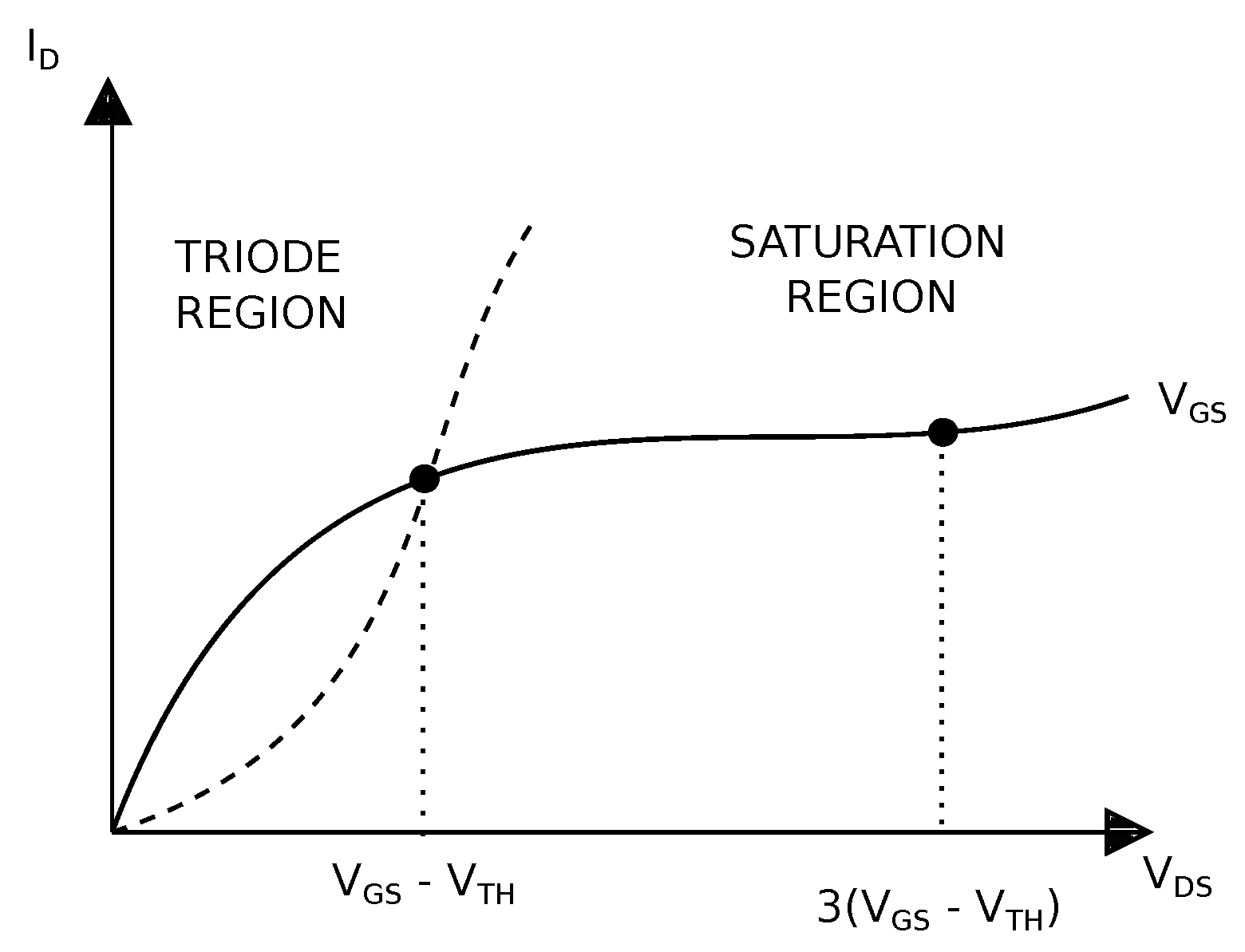
One of the main problems in sizing analog ICs is guaranteeing DCOP conditions of the MOS transistors. If a MOS transistor is not operating in the specific region, the circuit will not have the desired performance, thus affecting the output characteristics. Seminal CMOS design textbooks like Reference [31], provide guidelines to set the DCOP in a desired region. In an OTA, the MOS transistors operate in the saturation region, as shown in Figure 1, which necessary condition accomplishes (1). However, a bad sizing may lead the DCOP being located in the limit with the triode region, so that a slight variation of the voltages can lead the DCOP to be in the triode or cut-off region. In this manner, to guarantee that the MOS transistor works in the saturation region, we propose accomplishing (
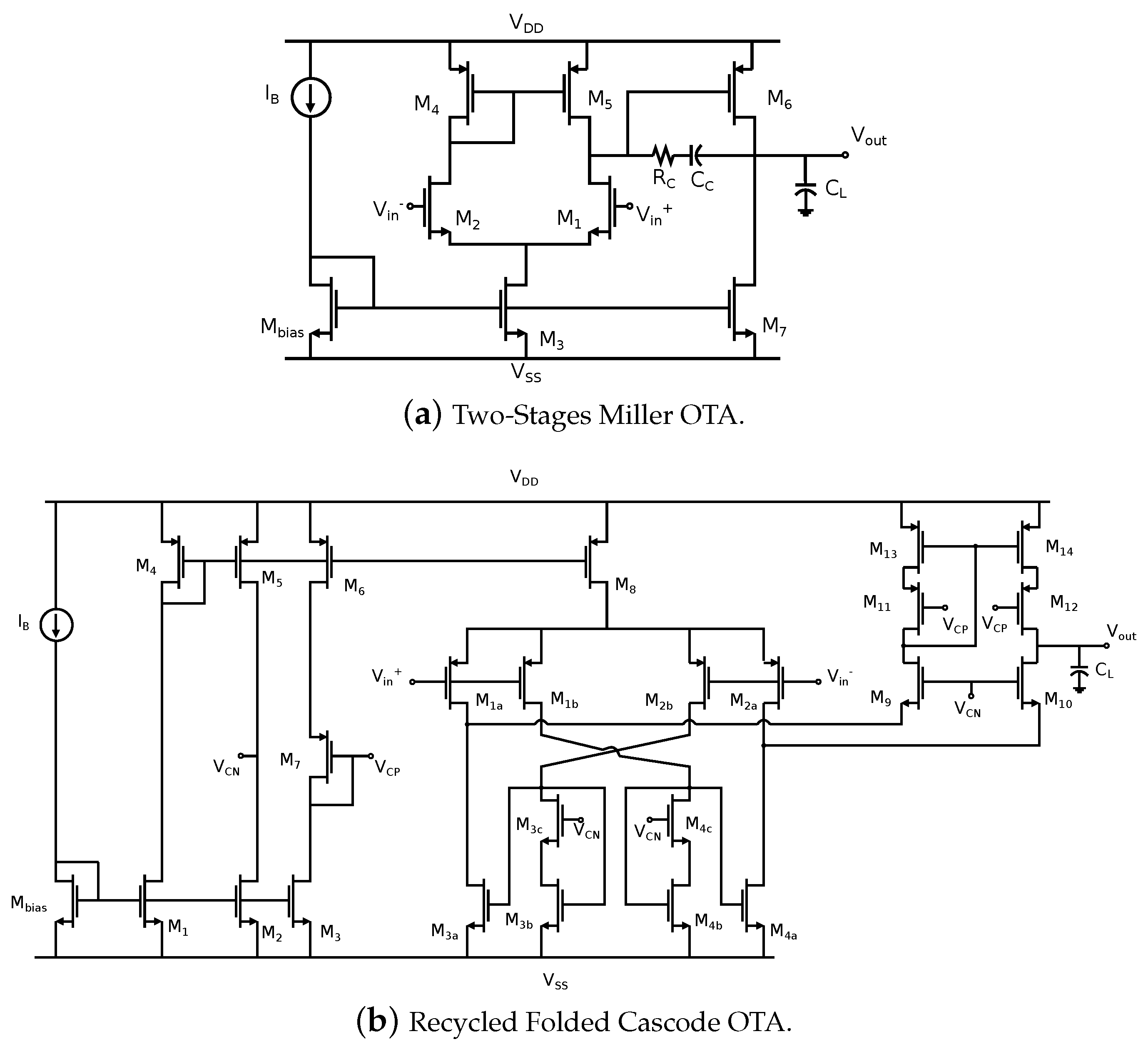
2), which is evaluated within PSO and MOL by introducing a procedure to handle this constraint. The OTAs used as cases of study are shown in Figure 2, which will be sized using CMOS technology of 180 nm, to accomplish a differential gain ≥ 60 dB and other performances to improve two figures of merit that are given in the following sections.
V D S > V G S V T H
V D S 3 ( V G S V T H ) .
As mentioned above, we show the application of PSO and MOL algorithms to maximize GBW of the two OTAs shown in Figure 2, the contribution focus on guaranteeing that all MOS transistors work in saturation region accomplishing (2). Both metaheuristics link SPICE to evaluate electrical characteristics of each OTA. Our proposed procedure for handling constraints in the sizing problem by applying PSO and MOL is formulated as follows:
Search for the widths ( W i ) and lengths ( L i ) of each MOS transistor in a CMOS OTA, such that:
Maximize the GBW product of the OTA,
subject to: V D S 3 ( V G S V T H ) , for each MOS transistor, and amplifier’s DC gain ≥ 60 dB, phase margin (PM) 45 , common-mode rejection ratio (CMRR) ≥ 60 dB, power supply rejection ratio (PSRR) 60 dB, and slew rate (SR) 10 v / μ s .
It is worthy mentioning that a maximization problem can be transformed to a minimization one by multiplying by minus one the desired objective. In this case, the maximization of GBW can be transformed to the minimization of −GBW.

3. PSO and MOL Algorithms

The history of PSO began from 1995, and nowadays it has been widely applied to size analog ICs [32,33,34], but still several open problems need attention [35]. The MOL algorithm has also shown good results in optimizing electric systems like in [36].

3.1. Particle Swarm Optimization Algorithm

PSO is based on a mathematical model developed by Kennedy and Eberhart in 1995 [35]. It describes the social behavior of birds or fishes. The model is based on the basic principles of self-organization that are used to describe complex systems. PSO is one of the most used mono-objective metaheuristics due to its success in solving optimization problems. As detailed in Reference [37], it starts from a set of randomly distributed particles in a limited search space. These particles have an initial position and velocity that are represented by simple mathematical expressions. These expressions suggest the movement of each particle towards the best position as an individual and the best global position, besides there are different variants using different update rules. The general idea is to initialize a set of particles in a search space, this gives the particles a favorable initial position, in addition an initial velocity vector is assigned, which allows the particles to change their position in each iteration while the speed is adjusted depending on some random parameters. Each particle can remember its best position and recognize if its current position is the best among the other particles, that is, the best global. The particles have to be updated according to their positions and past speeds. Mathematically, the updating equations are given in (3) and (4),
v i ( t + 1 ) = v i ( t ) + c 1 rand ( ) ( p b e s t ( t ) p i ( t ) ) + c 2 rand ( ) ( g b e s t ( t ) p i ( t ) )
p i ( t + 1 ) = p i ( t ) + v i ( t + 1 ) ,
where v i ( t + 1 ) and p i ( t + 1 ) represent the velocity and position of the particle in the i t h iteration, respectively; rand() is a function that returns uniform random real number values between 0 and 1; p b e s t and g b e s t represent the best position of the particle and the best global position among all the particles; c 1 and c 2 are two parameters that represent the confidence of the particle itself (cognition) and in the swarm (social behavior), respectively. These last constants are the most relevant in (3), according to a set of tests it was found that the higher the constants the faster the convergence will be. As mentioned in [35], the constants c 1 and c 2 have values that may improve the convergence, but it depends on the kind of problem. As already shown in [37], the PSO algorithm works fine if these constants are set to c 1 = c 2 = 2 .

3.2. Many Optimizing Liaisons Algorithm

MOL is a variant of PSO that is based on eliminating the best known position of the particle p b e s t in (3), which updates to (5). This variant behaves similarly or better than the PSO algorithm, where it proposes several combinations for the MOL parameters w, c 2 , given in (5), and the number of individuals (particles) for different problems, and thus one calibrates the algorithm depending on the dimensions of the problem and the number of evaluations of the objective function. MOL is a purely social algorithm tending to follow the best swarm’s particle ( g b e s t ), thus when the inertia coefficient w = 1 , it restricts the particles exploring better solutions in the search space, so that a challenge is finding the appropriate w value that allows the particles exploring different directions to find better solutions in the entire search space, in addition to maintain the velocity’s limits in a previously defined range. In this work the MOL parameters are set to w = 0.31 and c 2 = 2.03 .
v i ( t + 1 ) = w v i ( t ) + c 2 rand ( ) ( g b e s t ( t ) p i ( t ) ) .

4. Sizing OTAs by PSO and MOL to Improve DCOP Conditions

The pseudo-code provided in [38] associated to PSO algorithm, is used herein and it is adapted to size the two CMOS OTAs shown in Figure 2. The evaluation process links SPICE, which data is manipulated through writing and reading text-files that contain the descriptions and analyses of the CMOS OTAs. The pseudo-code of PSO is given in Algorithm 1, where one can see the call to SPICE and the verification of the DCOP conditions of the MOS transistors to guarantee that they are in saturation. The only difference between PSO and MOL algorithms in the pseudo-code is when the velocity of the particle is updated, in this case, the pseudo-code of MOL is the same as PSO but replacing (3) by (5).
An OTA must guarantee high differential-mode gain under the condition that all MOS transistors operate in saturation according to (2). If all MOS transistors are in the appropriate DCOP condition, then the OTA sized solutions are feasible. In this manner, and based on the selection mechanism given in [39], to select the best particle our proposed handling of constraints performs the following procedure: If two particles that satisfy (2) are compared, the particle with the highest GBW is chosen, for the case when one particle satisfies (2) and the other not, choose the one that satisfies (2). Finally, if none of the particles satisfy (2), the particle with more MOS transistors accomplishing the DCOP conditions is chosen. This constraint handling is used each time a particle is updated in both the PSO and MOL algorithms.
Algorithm 1 PSO
1:
procedurePSO( n P o p , M a x I t )
2:
    Generate the input file of the OTA (netlist) according to SPICE
3:
    for i = 1 : n P o p do
4:
        Initialize randomly the design variables: width (W), (L) of the MOS transistors and the bias current ( I B )
5:
        Replace randomly the design variables into the netlist
6:
        Simulate the OTA i in SPICE
7:
        Get the electrical characteristics of the output file ( * . l i s t ) according to SPICE
8:
        Calculate the constraints with respect to the electrical characteristics and update the p b e s t particle
9:
        Update the g b e s t particle by checking the constraints.
10:
    end for
11:
    for i t = 1 : M a x I t do
12:
        for i = 1 : n P o p do
13:
           Copy particle i to p
14:
           Update the particle p velocity according to (3)
15:
           Update the particle p position (design variables) according to (4)
16:
           Replace the new design variables into de netlist
17:
           Simulate the OTA p in SPICE
18:
           Compare particles i and p
19:
           Update p b e s t and g b e s t particles by checking the constraints.
20:
        end for
21:
    end for
22:
end procedure
The netlist of the OTAs is generated according to SPICE, and the design variables W and L are encoded by integer numbers, as already shown in [18]. An additional design variable is the bias current that is labeled as I B in the two OTAs shown in Figure 2 between 10 μ A and 100 μ A. W is set between 10 and 1500, and are scaled to microns within SPICE by using the command . o p t i o n s c a l e . The scale is equated to 0.09 μ within SPICE, which is equivalent to the lambda of the CMOS technology of 180 nm. The length of the MOS transistor L is set between 2 and 10, and also is scaled to the lambda of the technology. An example of using these commands within SPICE is given below.
.option scale = 0.09 u
.param W1 = 56 W2 = 67 L = 4 IB = 50.
In the case that PSO or MOL produce a negative number when evaluating (3), it is replaced by the minimum value of the search space of W. The DCOP condition is guaranteed by extracting the values of V D S , V G S and V T H for each MOS transistor and from the output text-file provided by SPICE, with extension. lis. In this text-file, each MOS transistor (M1, M2, …, M6) has currents I d in the ranges of microns ( μ ), and the voltages in milli-volts (m). Each column is verified to accomplish that the ratio in (2) is greater than 3 (see 3( V G S V T H ) in Figure 1), so that the DCOP of the MOS transistor is in saturation. If the ratio is lower than 3, the MOS transistor is in triode region, which is not appropriate for the OTAs. If all MOS transistors are in saturation, PSO and MOL algorithms evaluate the GBW, and updates the best individual associated to the highest GBW of the population.
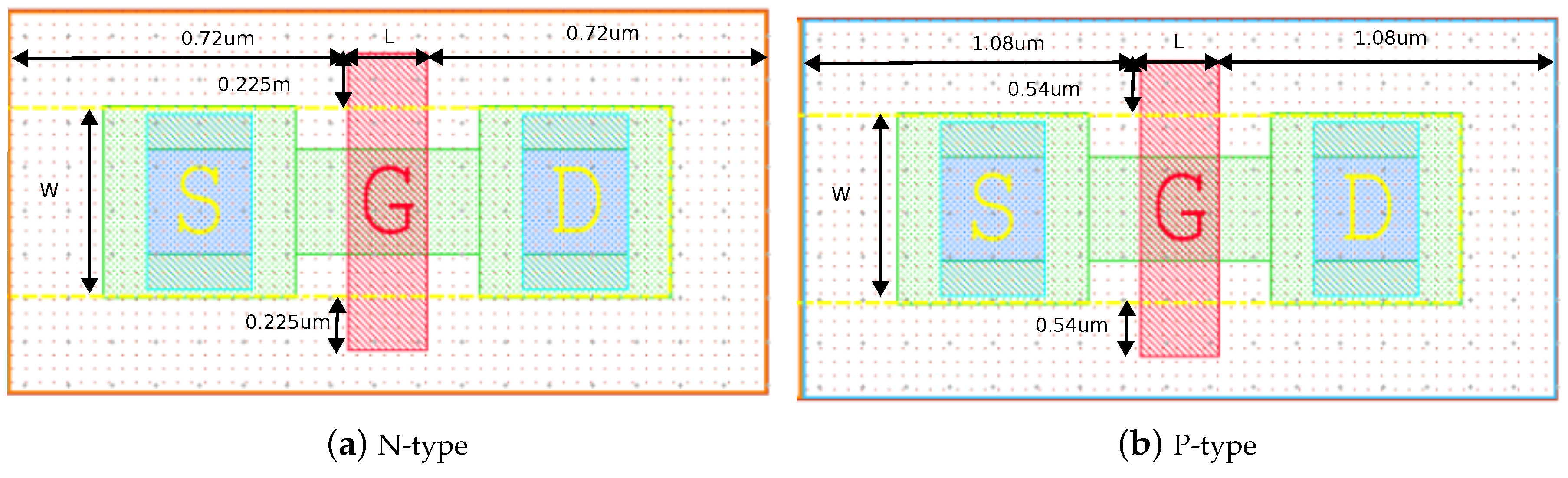
In this paper, the process to calculate the silicon area of each MOS transistor is based on the layout and the smallest W and L allowed by the technology, and scaled by λ , which is 0.09 μ m. Figure 3 shows the minimum dimensions in λ occupied by an N-type and a P-type MOS transistor. As one sees, the estimation of the area is performed considering W and L of the transistor. The equations that estimate the area of an N-type and a P-type MOS transistor are given in (6) and (7), respectively. Therefore, the estimated total area is associated to the sum of each of the MOS transistors that are included into the OTAs shown in Figure 2. It is important to mention that these equations are only an estimate, since the area of the contacts and the metallic interconnections were not considered.
A r e a N t r a n s i s t o r = ( W λ + 5 λ ) ( L λ + 16 λ )
A r e a P t r a n s i s t o r = ( W λ + 12 λ ) ( L λ + 24 λ ) .

5. Feasible Sized Solutions Provided by PSO and MOL

Both PSO and MOL were executed during 30 runs to size the CMOS Miller and RFC-OTAs already shown in Figure 2, and 100 generations were considered for each run with populations of 10 particles. The characteristics of the two solved problems are summarized in Table 1. Both sizing algorithms guarantee DCOP conditions accomplishing (2).
The feasible solutions (sizes) can be compared through evaluating a figure of merit (FoM). In this case, and according to [27], the criteria is that the higher the value of the FoM, the better the performance of the OTA. As the GBW is the objective function, the small-signal F o M s [5,40,41], is evaluated by (8), and the large-signal F o M l by (9).
F o M s = GBW × C L I B
F o M l = S R × C L I B .
An important aspect and one of the advantages of sizing applying metaheuristics is that it allows us to obtain a set of solutions that satisfy the established specifications. These solutions are called feasible solutions. On the other hand, by having a set of feasible solutions and not a single solution, it allows the designer to choose the design that best suits their requirements.

5.1. Sizing the Two-Stage Miller Amplifier

In both PSO and MOL the direction of the particle gradually changes to move in the direction of the best found positions, looking in its vicinity and potentially discovering better positions according to Equations (3)–(5). In sizing CMOS OTAs, the position of the particle represents the W, L and I B that are being updated in order to find the best GBW product. According to the constraint-handling mechanism implemented herein, the best particle is the one that meets the greatest number of constraints, lowest silicon area and differential-mode gain of at least 60 dB. This is shown in 
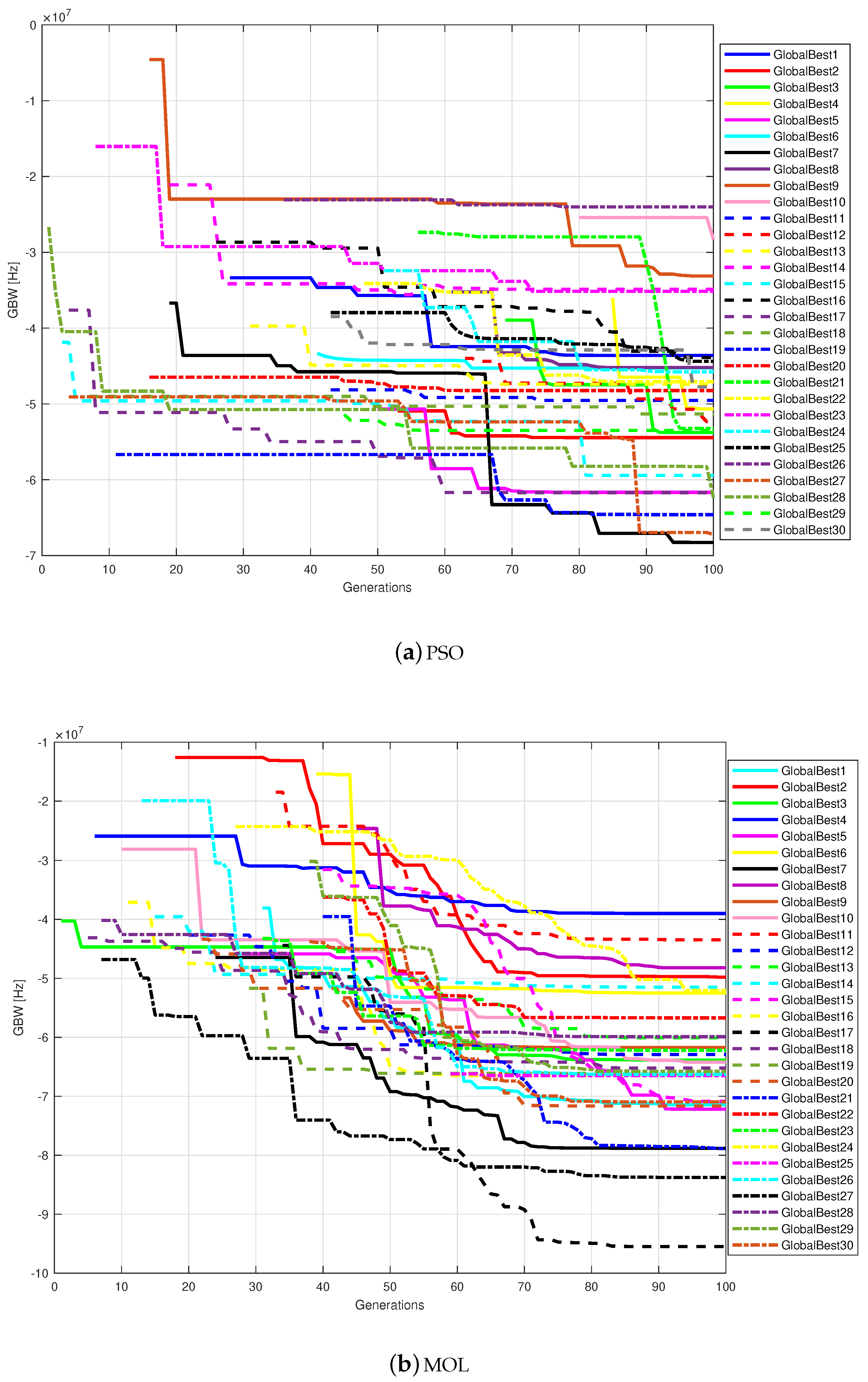
Figure 4 where GBW is evaluated for 10 particles at each generation for 30 runs. One can see the evolution of the best global particle, when the problem formulation is oriented to minimize GBW. These results are summarized in Table 2 and Table 3 for PSO and MOL, respectively. The gain constraint given in Table 1 is accomplished as shows in the first row of each Table. The objective function GBW values are listed in the second row. The other performances are listed in the Tables above the evaluation of the F o M s and F o M l . Below the figures of merit we list the best sizes for each run that are associated to the MOS transistors, and the bias current in the last row of each Table.
As recommended in Reference [35], the parameters w and c 2 of the MOL algorithm must be tuned according to the problem at hand. In this work they are set to w = 0.31 and c 2 = 2.03 , and the same parameters are used to size the RFC-OTA.

5.2. Recycled Folded Cascode Operational Transconductance Amplifier

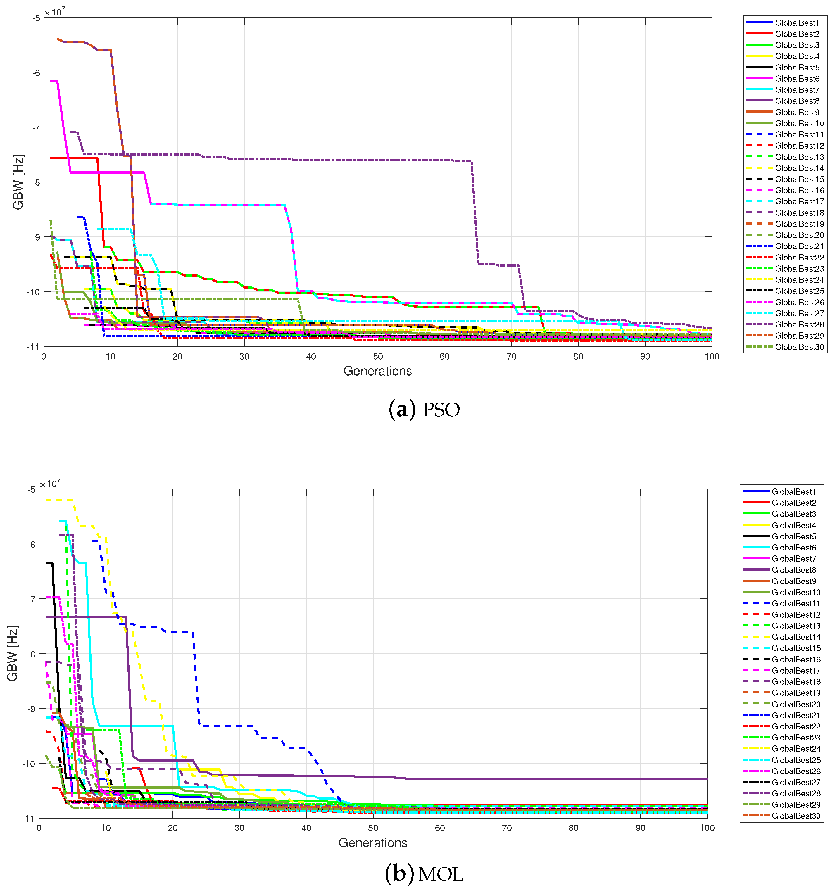
Figure 5 shows the behavior of the best global particle for 30 runs using the PSO and MOL algorithms to size the RFC-OTA. This figure just shows only the feasible solutions. For both PSO and MOL algorithms, it takes some generations to obtain these feasible solutions. It can be appreciated that unlike the Miller OTA, the feasible solutions of the RFC-OTA are more dispersed, however, in each run both the objective function and constraints are fulfilled around 100 generations.
Table 4 and Table 5 show the feasible electrical characteristics of the RFC-OTA applying PSO and MOL. These values demonstrate that the sizes found by the particles meet all the constraints that were determined in the problem definition. A key point for these constraints to be fulfilled and the objective function to be improved is the way the constraints handling is performed. In this work, at the beginning the algorithm looks for the solutions that best comply with the constraints and then is responsible for improving the objective function. A comparison among the solutions generated by PSO and MOL for the 30 runs and for both OTAs is shown in 
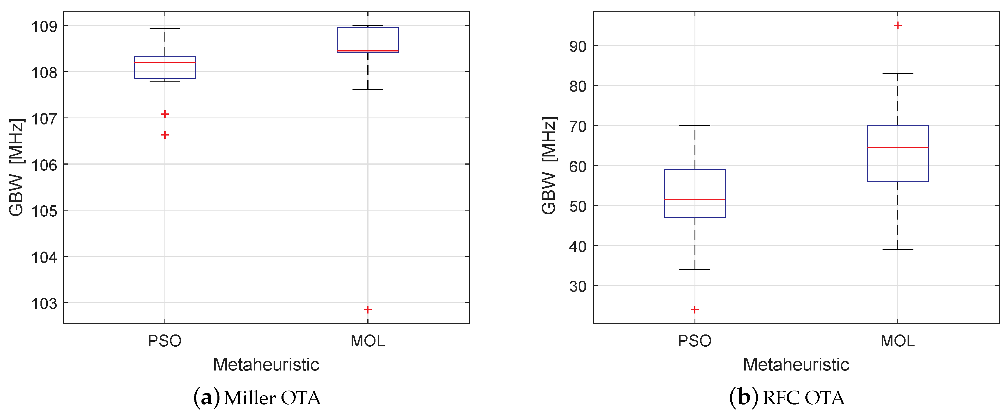
Figure 6. It can be appreciated that MOL finds better feasible solutions on average (with greater GBW), and also it can find better isolated solutions.
As one can infer, sizing the RFC-OTA requires a higher computational effort than the OTA Miller. However, the application of PSO and MOL, provided better figures of merit compared to the literature. For example: according to Table 4 and Table 5, the F o M s value is 3361.9 and 4750 by applying PSO and MOL, respectively. These values are much better than the reported one in [21] as 1029, [3] as 2642, [23] as 260.4, [42] as 1920, [43] as 2101, [27] as 2365, [44] as 404.44, and in [45] as 2540. Thus demonstrating that our proposed sizing approach by guaranteeing DCOP conditions is capable of achieving better results than those found in the state-of-the-art.

5.3. Monte Carlo and PVT Analyses

Montecarlo is a statistical analysis where V T H , T O X , W, L and mismatch are varied randomly in the circuit devices. Nevertheless, to guarantee the robustness of the integrated circuits it is also necessary to carry out a process-voltage-temperature (PVT) analysis, since it performs variations in voltage and/or temperature without taking into account mismatch, and the process variation includes corner analysis.

5.3.1. Monte Carlo Analysis

Monte Carlo method is quite important in the statistical analysis of integrated circuits, besides there is no equation for the forward relation between the simulated data and the model parameters. Therefore, Monte Carlo simulations are commonly performed to analyze experimental data and eventually to acquire predictive capabilities. In this paper, Monte Carlo analysis was performed to the 30 optimized results shown in Figure 4 and Figure 5 during 1000 runs. The data from each Monte Carlo simulation was processed to find statistical data, such as the mean and standard deviation. From these data we selected the 10 best solutions shown in Table 2, Table 3, Table 4 and Table 5. The criterion for selecting these solutions were those with greater GWB average and low standard deviation.
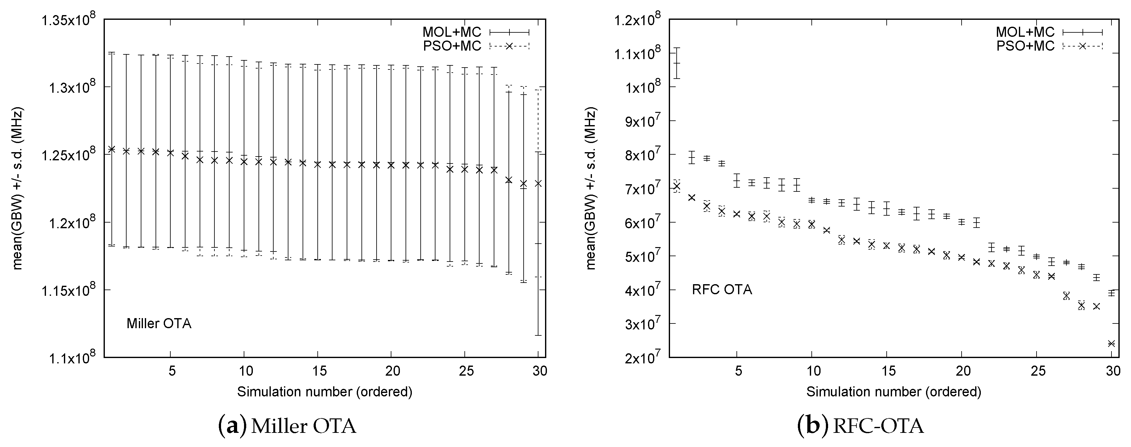
The statistical comparison of all Monte Carlo solutions during 1000-runs was carried out, and the results are shown in Figure 7, where the mean and standard deviation of each OTA are plotted when applying PSO and MOL. An important aspect that should be highlighted is that the sizing of the RFC-OTA is more complex than that of the Miller OTA. However, the variability of the Monte Carlo analysis does not affect the best solution obtained by PSO and MOL.
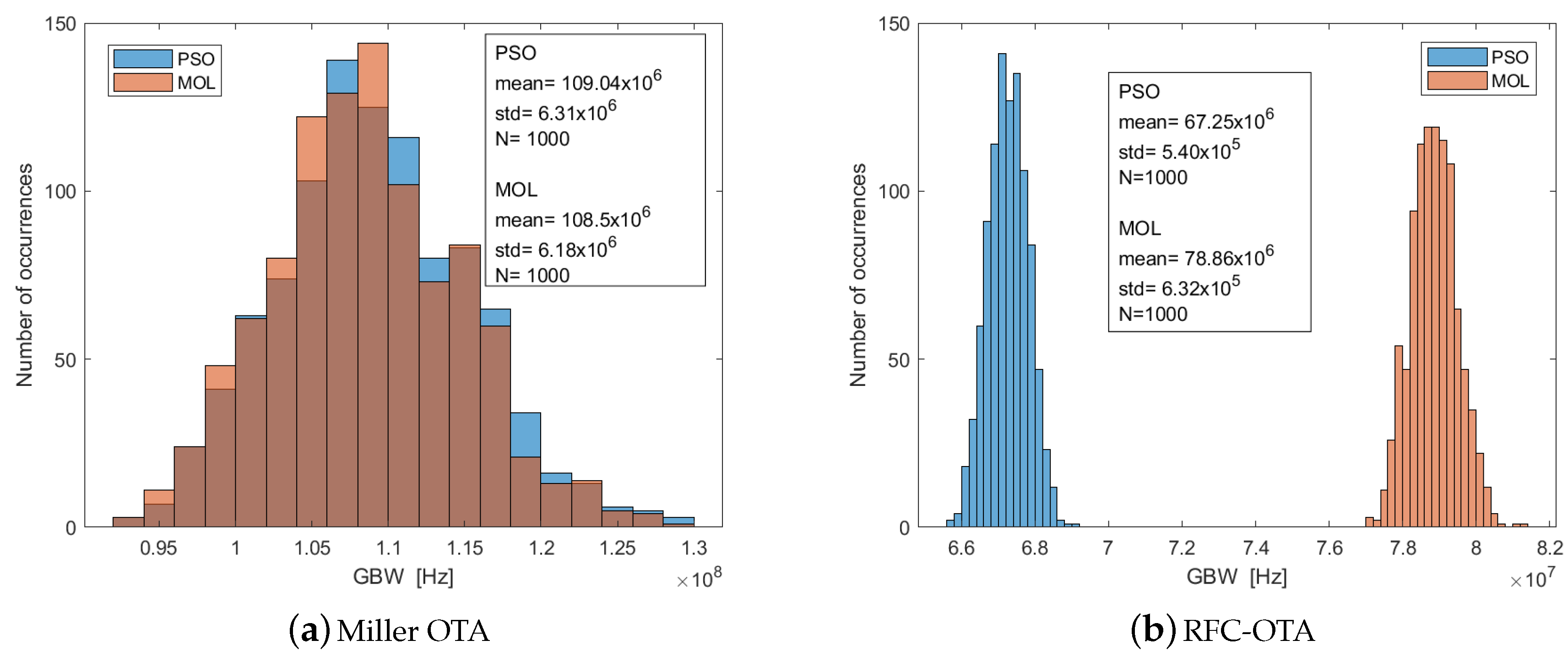
From the above analysis, the best solutions are shown in Figure 8, where one can see the Monte Carlo simulation results for the GBW of the Miller and RFC-OTA, respectively. The results provided by PSO and MOL are almost similar in Figure 8a for the Miller-OTA, but as the RFC-OTA is more complex, PSO and MOL provided different results as shown in Figure 8b. The simulations were carried out assuming 10% deviation (with a Gaussian distribution) in W and L for all the MOS transistors.

5.3.2. PVT Analysis

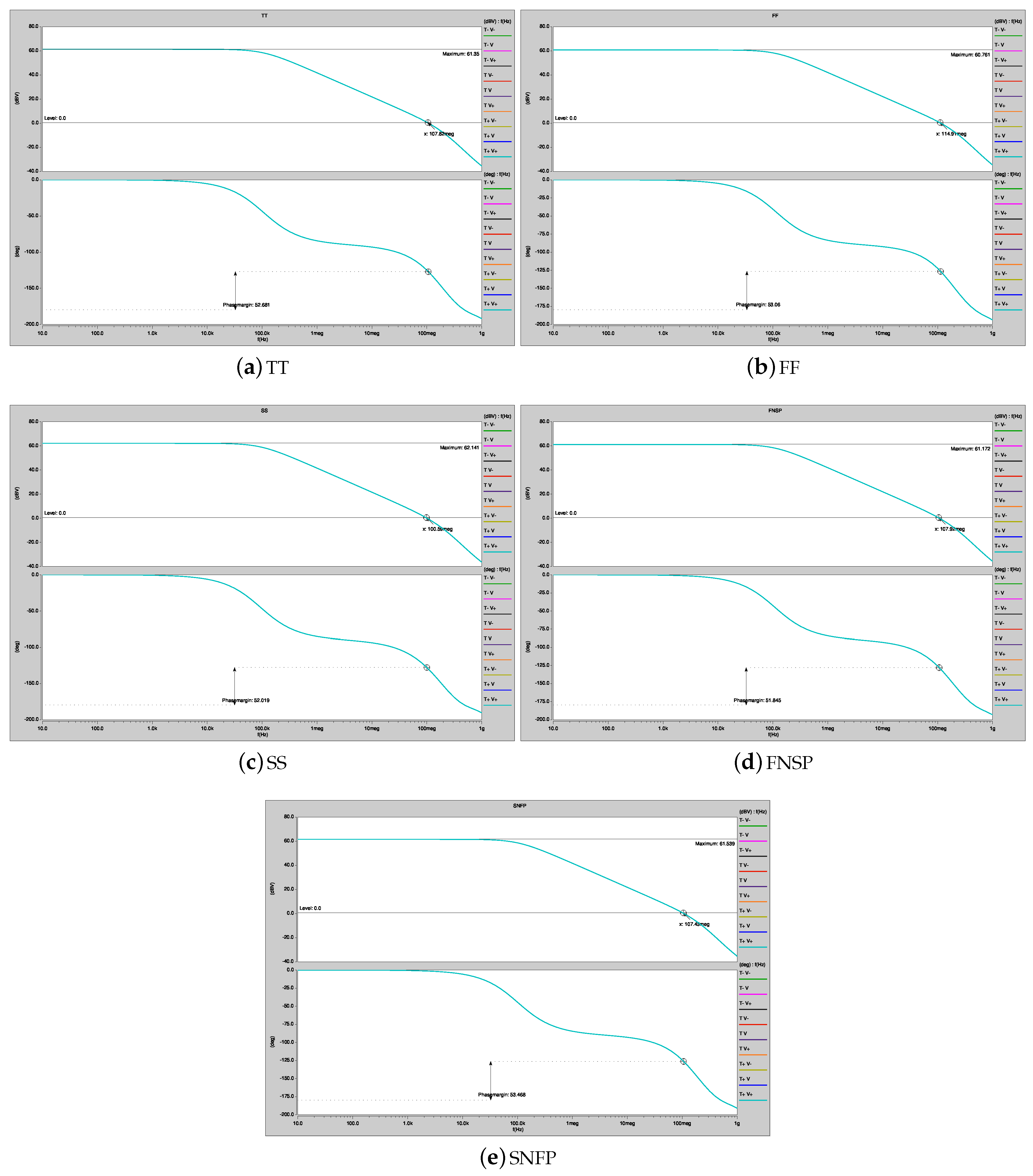
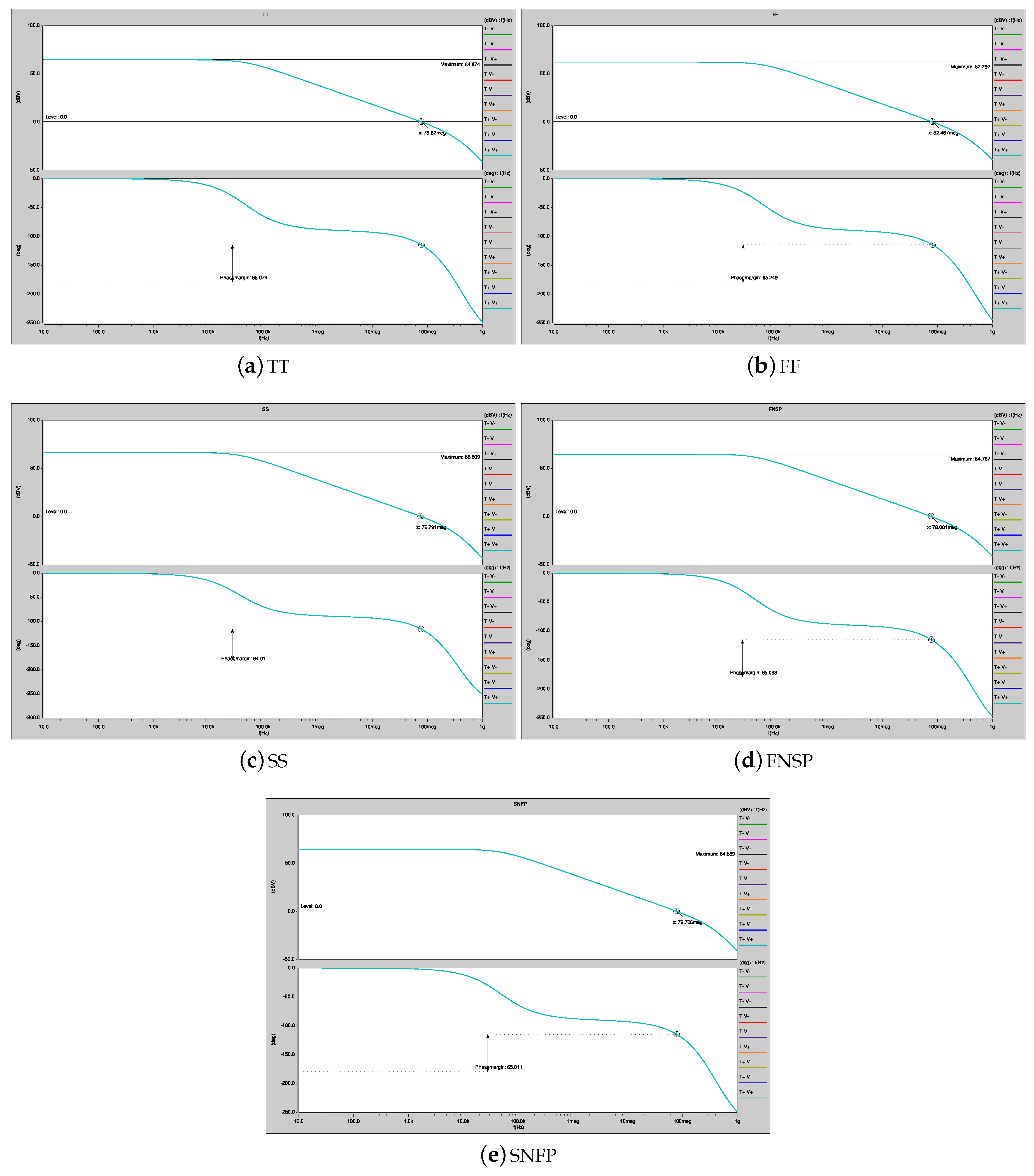
The analog IC design faces a lot of challenges as ensuring that all target specifications are achieved. In this manner, the feasible solutions provided by a metaheuristic yet need to satisfy other statistical analyses like PVT variations. It is worth mentioning that process variations depend on global variations such as wafer imperfections or chemical processes, voltage variations are due to untimely changes in the supply voltages that affect the DCOP of the transistors, and temperature variations occur in most cases when the circuit is near heat-sources or by the same energy of the circuit. In this manner, and as mentioned in Section 2, guaranteeing the DCOP of each transistor is an important aspect because it influences directly the performance of the CMOS OTA. Currently, the conditions in which the ICs work are not ideal, therefore they must maintain their electrical characteristics despite being affected by PVT variations. In this manner, we include PVT analysis to demonstrate that the feasible solutions of the OTAs accomplish the condition given in (2). Therefore, the PVT simulation results for the Miller and RFC-OTA are shown in Figure 9 and Figure 10, and they confirm that the GBW remains within a stable range, as does the DC gain because the DCOP was guaranteed during the optimization. Each figure shows one of the corners of the typical-typical (TT), fast-fast (FF), slow-slow (SS), fastN-slowP (FNSP) and slowN-fastP (SNFP) cases. Each corner case is performed by varying the voltage by ± 10 % of the supply voltage, and the temperature by varying from −20 degrees, 60 degrees to 120 degrees.
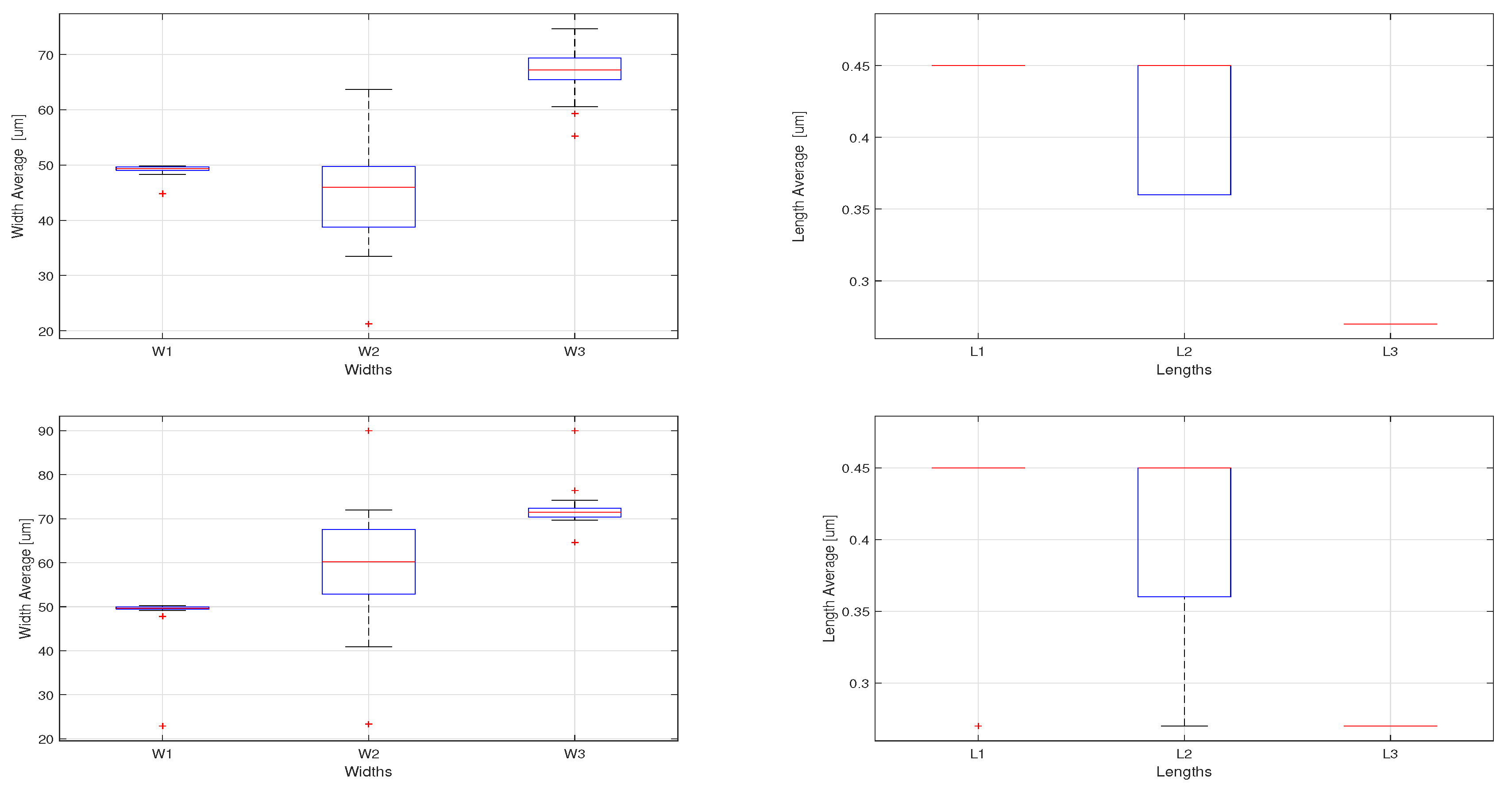
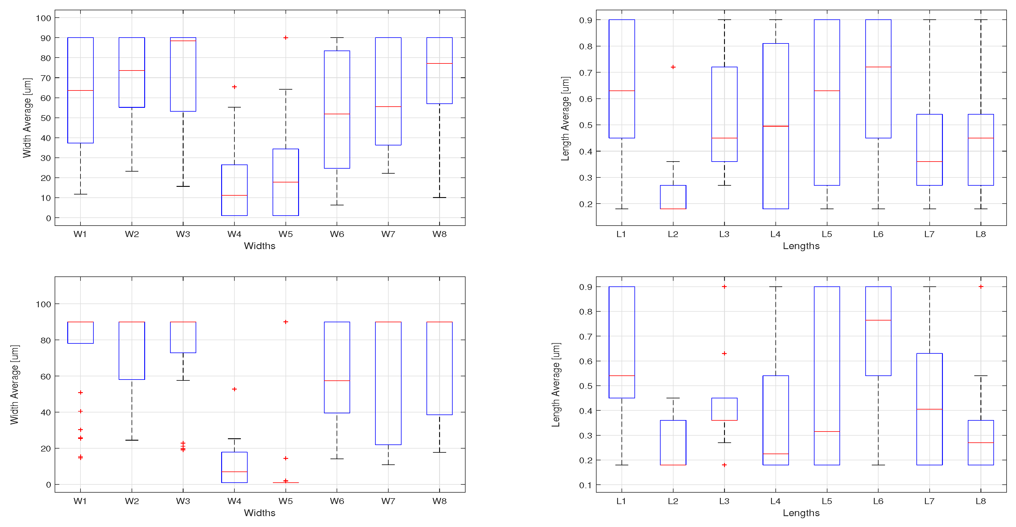
In the optimization process, the OTA Miller was encoded with three widths and three lengths, and the RFC-OTA was encoded with eight widths and eight lengths. The feasible sizes solutions have the ranges shown for the OTA Miller in Figure 11. In the case of the RFC-OTA, the ranges of the feasible sizes are shown in Figure 12. These box plots show the median and quartiles of the data, so that one can choose design variables in the less sensitive values. For example, in the second rows of Figure 11 and Figure 12, one can conclude that the more sensitive values are associated to the length L1 and L3, which were encoded with M1, M2, M4, M5 and M7 according to Table 2. Therefore, this length needs to maintain a value of about 0.45 μ m and 0.18 μ m respectively, in order to achieve the objectives and constraints described in the problem definition.
Analyzing the results of the RFC OTA simulations and Figure 12, it is possible to identify the transistors that are more sensitive. They are the current mirror that bias the differential pair. This is because the bias V c n must bias the current mirrors in cascode configuration. Therefore, to satisfy the objectives it is necessary that the widths and lengths: W4, W5, L4 and L5, remain around the values shown in Figure 12, since outside these ranges the circuit could not meet the target specifications. Some recent research has been done by applying regression techniques [46], and it can be combined to improve the sizing of MOS amplifiers to enhance important characteristics as slew rate [47].

6. Conclusions

Sizing CMOS OTAs is very challenging because there are many target specifications that must be accomplished, and the design variables can have sparse search space ranges. This work highlighted the usefulness of applying metaheuristics like PSO and MOL to size OTAs using CMOS technology, and linking a circuit simulator like SPICE to evaluate electrical characteristics that also have sparse search space ranges. The main goal was oriented to guarantee DCOP conditions of all MOS transistors, and it was accomplished in all the optimization cases applying PSO and MOL. We proposed that the DCOP can be guaranteed if the drain-to-source voltage V D S is at least three times greater than the difference between the gate-to-source and threshold voltages: V G S V T H . This condition was programmed into the PSO and MOL algorithms as our proposed procedure for handling constraints. The feasible sizes of the MOS transistors provided by PSO and MOL were tested under Monte Carlo and PVT variations to guarantee robust design of the Miller OTA and the RFC-OTA. We showed the behavior of both metaheuristics, PSO and MOL during 30 runs, using 10 particles in each run and optimizing GBW over 100 generations. The optimization results confirmed the suitability of applying metaheuristics in the sizing of analog ICs, and the usefulness of our proposed procedure for the handling of constraints to guarantee appropriate DCOP conditions of the feasible sized solutions. As one can infer, both PSO and MOL can be extended to perform the optimal sizing of other integrated circuits, basically one must know the features and target specifications of each particular circuit, so that one can set the design variables, objectives, constraints and corresponding analyzes into the metaheuristics to perform the optimization. Finally, it is worthy mentioning that the optimal sizing by PSO and MOL does not require a particular technology, instead one can use non-CMOS technologies according to the designer’s requirements

Author Contributions

Investigation, E.T.-C., M.A.V.-P. and L.G.d.l.F.; Writing—review and editing, E.T.-C., M.A.V.-P. and L.G.d.l.F. All authors have read and agreed to the published version of the manuscript.

Funding

This research received no external funding.

Conflicts of Interest

The authors declare no conflict of interest.

References

  1. Ramos, F.G.R.; Mussolini, T.P.; Moreno, R.L.; Pimenta, T.C. A CMOS temperature-independent current reference optimized for mixed-signal applications. Integration 2019, 66, 88–95. [Google Scholar] [CrossRef]
  2. Afacan, E. Inversion coefficient optimization based Analog/RF circuit design automation. Microelectron. J. 2019, 83, 86–93. [Google Scholar] [CrossRef]
  3. Feizbakhsh, S.V.; Yosefi, G. An enhanced fast slew rate recycling folded cascode Op-Amp with general improvement in 180 nm CMOS process. AEU-Int. J. Electron. Commun. 2019, 101, 200–217. [Google Scholar] [CrossRef]
  4. Jomehei, M.G.; Sheikhaei, S. A low-power low-noise CMOS bio-potential amplifier for multi-channel neural recording with active DC-rejection and current sharing. Microelectron. J. 2019, 83, 197–211. [Google Scholar] [CrossRef]
  5. Ghosh, S.; De, B.P.; Kar, R.; Mal, A.K. Symbiotic organisms search algorithm for optimal design of CMOS two-stage op-amp with nulling resistor and robust bias circuit. IET Circuits Devices Syst. 2019, 13, 679–688. [Google Scholar] [CrossRef]
  6. Hemmati, M.J.; Dehghani, R.; Hakimi, A. A low-voltage swing-enhanced Colpitts CMOS LC-QVCO based on first-harmonics coupling. Microelectron. J. 2019, 85, 6–16. [Google Scholar] [CrossRef]
  7. Passos, F.; Martins, R.; Lourenço, N.; Roca, E.; Póvoa, R.; Canelas, A.; Castro-López, R.; Horta, N.; Fernández, F.V. Enhanced systematic design of a voltage controlled oscillator using a two-step optimization methodology. Integration 2018, 63, 351–361. [Google Scholar] [CrossRef] [Green Version]
  8. Kote, V.; Kubacak, A.; Vacula, P.; Jakovenko, J.; Husak, M. Automated pre-placement phase as a part of robust analog-mixed signal physical design flow. Integration 2018, 63, 18–30. [Google Scholar] [CrossRef]
  9. Maji, K.; De, B.; Kar, R.; Mandal, D.; Ghoshal, S. CMOS analog amplifier circuits design using seeker optimization algorithm. IETE J. Res. 2019, 1–10. [Google Scholar] [CrossRef]
  10. Shokouhifar, M.; Jalali, A. Simplified symbolic transfer function factorization using combined artificial bee colony and simulated annealing. Appl. Soft Comput. 2017, 55, 436–451. [Google Scholar] [CrossRef]
  11. De Venuto, D.; Mezzina, G.; Rabaey, J. Automatic 3D Design for Efficiency Optimization of a Class E Power Amplifier. IEEE Trans. Circuits Syst. II Express Briefs 2018, 65, 201–205. [Google Scholar] [CrossRef]
  12. Boni, A.; Giuffredi, L.; Pietrini, G.; Magnanini, A.; Tonelli, M. Design-oriented model for power-driven design optimization of SC Sigma-Delta modulators. Int. J. Circuit Theory Appl. 2018, 46, 707–728. [Google Scholar] [CrossRef]
  13. Castejón, F.; Carmona, E.J. Automatic design of analog electronic circuits using grammatical evolution. Appl. Soft Comput. 2018, 62, 1003–1018. [Google Scholar] [CrossRef]
  14. Moreto, R.; Thomaz, C.; Gimenez, S. Impact of designer knowledge in the interactive evolutionary optimisation of analogue CMOS ICs by using iMTGSPICE. Electron. Lett. 2018, 55, 16–18. [Google Scholar] [CrossRef]
  15. Martins, R.; Lourenco, N.; Horta, N.; Yin, J.; Mak, P.I.; Martins, R.P. Many-Objective Sizing Optimization of a Class-C/D VCO for Ultralow-Power IoT and Ultralow-Phase-Noise Cellular Applications. IEEE Trans. Large Scale Integr. (VLSI) Syst. 2019, 27, 69–82. [Google Scholar] [CrossRef]
  16. Passos, F.; Gonzalez-Echevarria, R.; Roca, E.; Castro-López, R.; Fernandez, F. A two-step surrogate modeling strategy for single-objective and multi-objective optimization of radiofrequency circuits. Soft Comput. 2019, 23, 4911–4925. [Google Scholar] [CrossRef] [Green Version]
  17. De, B.P.; Maji, K.B.; Kar, R.; Mandal, D.; Ghoshal, S.P. Design of Optimal CMOS Analog Amplifier Circuits Using a Hybrid Evolutionary Optimization Technique. J. Circuits Syst. Comput. 2018, 27, 1850029. [Google Scholar] [CrossRef]
  18. Sanabria-Borbón, A.; Tlelo-Cuautle, E. Sizing analogue integrated circuits by integer encoding and NSGA-II. IETE Tech. Rev. 2018, 35, 237–243. [Google Scholar] [CrossRef]
  19. Garde, M.P.; Lopez-Martin, A.; Carvajal, R.G.; Ramírez-Angulo, J. Super Class-AB Recycling Folded Cascode OTA. IEEE J. Solid-State Circuits 2018, 53, 2614–2623. [Google Scholar] [CrossRef]
  20. Aminzadeh, H.; Dashti, M.A. Dual loop cascode-Miller compensation with damping factor control unit for three-stage amplifiers driving ultralarge load capacitors. Int. J. Circuit Theory Appl. 2019, 47, 1–18. [Google Scholar] [CrossRef] [Green Version]
  21. Yosefi, G. The high recycling folded cascode (HRFC): A general enhancement of the recycling folded cascode operational amplifier. Microelectron. J. 2019, 89, 70–90. [Google Scholar] [CrossRef]
  22. Khade, A.S.; Vyas, V.; Sutaone, M. Performance enhancement of advanced recycling folded cascode operational transconductance amplifier using an unbalanced biased input stage. Integration 2019, 69, 242–250. [Google Scholar] [CrossRef]
  23. Lv, X.; Zhao, X.; Wang, Y.; Wen, B. An improved non-linear current recycling folded cascode OTA with cascode self-biasing. AEU-Int. J. Electron. Commun. 2019, 101, 182–191. [Google Scholar] [CrossRef]
  24. Garde, M.P.; Lopez-Martin, A.; Algueta, J.M.; Carvajal, R.G.; Ramirez-Angulo, J. Class AB amplifier with enhanced slew rate and GBW. Int. J. Circuit Theory Appl. 2019, 47, 1199–1210. [Google Scholar] [CrossRef]
  25. Cellucci, D.; Centurelli, F.; Di Stefano, V.; Monsurrò, P.; Pennisi, S.; Scotti, G.; Trifiletti, A. 0.6-V CMOS cascode OTA with complementary gate-driven gain-boosting and forward body bias. Int. J. Circuit Theory Appl. 2020, 48, 15–27. [Google Scholar] [CrossRef]
  26. Centurelli, F.; Monsurrò, P.; Trifiletti, A. High-gain, high-CMRR class AB operational transconductance amplifier based on the flipped voltage follower. Int. J. Circuit Theory Appl. 2019, 47, 499–512. [Google Scholar] [CrossRef]
  27. Veldandi, H.; Shaik, R.A. Low-voltage PVT-insensitive bulk-driven OTA with enhanced DC gain in 65-nm CMOS process. AEU-Int. J. Electron. Commun. 2018, 90, 88–96. [Google Scholar] [CrossRef]
  28. Carbajal-Gomez, V.H.; Tlelo-Cuautle, E.; Muñoz-Pacheco, J.M.; de la Fraga, L.G.; Sanchez-Lopez, C.; Fernandez-Fernandez, F.V. Optimization and CMOS design of chaotic oscillators robust to PVT variations. Integration 2019, 65, 32–42. [Google Scholar] [CrossRef]
  29. Guerra-Gomez, I.; Tlelo-Cuautle, E. Sizing analog integrated circuits by current-branches-bias assignments with heuristics. Elektron. Ir Elektrotechnika 2013, 19, 81–86. [Google Scholar] [CrossRef]
  30. Mallick, S.; Kar, R.; Ghoshal, S.; Mandal, D. Optimal sizing and design of CMOS analogue amplifier circuits using craziness-based particle swarm optimization. Int. J. Numer. Model. Electron. Netw. Devices Fields 2016, 29, 943–966. [Google Scholar] [CrossRef]
  31. Razavi, B. Fundamentals of Microelectronics; Wiley: Hoboken, NJ, USA, 2008. [Google Scholar]
  32. Asaithambi, S.; Rajappa, M. Swarm intelligence-based approach for optimal design of CMOS differential amplifier and comparator circuit using a hybrid salp swarm algorithm. Rev. Sci. Instrum. 2018, 89, 054702. [Google Scholar] [CrossRef] [PubMed]
  33. Maji, K.B.; Kar, R.; Mandal, D.; Ghoshal, S. Optimal design of low power high gain and high speed CMOS circuits using fish swarm optimization algorithm. Int. J. Mach. Learn. Cybern. 2018, 9, 771–786. [Google Scholar] [CrossRef]
  34. Singh, C.L.; Anandini, C.; Gogoi, A.J.; Baishnab, K. Automated sizing of low-noise CMOS analog amplifier using ALCPSO optimization algorithm. J. Inf. Optim. Sci. 2018, 39, 99–111. [Google Scholar] [CrossRef]
  35. Wang, D.; Tan, D.; Liu, L. Particle swarm optimization algorithm: An overview. Soft Comput. 2018, 22, 387–408. [Google Scholar] [CrossRef]
  36. Saha, N.; Panda, A.; Panda, S. Speed control with torque ripple reduction of switched reluctance motor by many optimizing liaison technique. J. Electr. Syst. Inf. Technol. 2018, 5, 829–842. [Google Scholar] [CrossRef]
  37. Kaveh, A. Advances in Metaheuristic Algorithms for Optimal Design of Structures; Springer: Berlin/Heidelberg, Germany, 2014. [Google Scholar]
  38. Particle Swarm Optimization in MATLAB. Available online: http://yarpiz.com/50/ypea102-particle-swarm-optimization (accessed on 22 May 2019).
  39. Cabrera, J.C.F.; Coello, C.A.C. Handling constraints in particle swarm optimization using a small population size. In Proceedings of the Mexican International Conference on Artificial Intelligence, Aguascalientes, Mexico, 4–10 November 2007; pp. 41–51. [Google Scholar]
  40. Mojarad, M.; Kamarei, M. Low-voltage high-gain large-capacitive-load amplifiers in 90-nm CMOS technology. AEU-Int. J. Electron. Commun. 2015, 69, 666–672. [Google Scholar] [CrossRef]
  41. Riad, J.; Estrada-López, J.J.; Sánchez-Sinencio, E. Classification and Design Space Exploration of Low-Power Three-Stage Operational Transconductance Amplifier Architectures for Wide Load Ranges. Electronics 2019, 8, 1268. [Google Scholar] [CrossRef] [Green Version]
  42. Zhang, Q.; Zhao, X.; Zhang, X.; Zhang, Q. Multipath recycling method for transconductance enhancement of folded cascade amplifier. AEU-Int. J. Electron. Commun. 2017, 72, 1–7. [Google Scholar] [CrossRef]
  43. Ragheb, A.; Kim, H. Ultra-low power OTA based on bias recycling and subthreshold operation with phase margin enhancement. Microelectron. J. 2017, 60, 94–101. [Google Scholar] [CrossRef]
  44. Wang, Y.; Zhang, Q.; Yu, S.S.; Zhao, X.; Trinh, H.; Shi, P. A Robust Local Positive Feedback Based Performance Enhancement Strategy for Non-Recycling Folded Cascode OTA. IEEE Trans. Circuits Syst. I Regul. Pap. 2020, 1–12. [Google Scholar] [CrossRef]
  45. Yan, Z.; Mak, P.I.; Martins, R. Double recycling technique for folded-cascode OTA. Analog Integr. Circuits Signal Process. 2012, 71, 137–141. [Google Scholar] [CrossRef]
  46. Sanabria-Borbón, A.C.; Soto-Aguilar, S.; Estrada-López, J.J.; Allaire, D.; Sánchez-Sinencio, E. Gaussian-Process-Based Surrogate for Optimization-Aided and Process-Variations-Aware Analog Circuit Design. Electronics 2020, 9, 685. [Google Scholar] [CrossRef] [Green Version]
  47. Zhao, X.; Zhang, Q.; Wang, Y.; Deng, M. Transconductance and slew rate improvement technique for current recycling folded cascode amplifier. AEU-Int. J. Electron. Commun. 2016, 70, 326–330. [Google Scholar] [CrossRef]
Figure 1. Direct current operating point (DCOP) regions in a MOS transistor plotting I D vs V D S .
Electronics 09 01027 g001
Figure 2. Topologies of the two complementary metal-oxide-semiconductor (CMOS) operational transconductance amplifiers (OTAs) used as case of study.
Electronics 09 01027 g002
Figure 3. Layout of the N-type and P-type MOS transistors.
Electronics 09 01027 g003
Figure 4. Evolution of the gain-bandwidth product (GBW) of the Miller OTA for 30 runs applying: (a) Particle swarm optimization (PSO) and (b) many optimizing liaisons (MOL).
Electronics 09 01027 g004
Figure 5. Global evolution of the GBW of the recycled-folded-cascode (RFC) OTA for 30 runs applying: (a) PSO and (b) MOL.
Electronics 09 01027 g005
Figure 6. Box plots of the behavior of the best feasible solutions applying PSO and MOL in the optimal sizing of the OTA Miller and RFC-OTA.
Electronics 09 01027 g006
Figure 7. Mean and standard deviation of the Monte Carlo simulation for all the 30 optimization runs.
Electronics 09 01027 g007
Figure 8. Monte Carlo simulations of the best solutions.
Electronics 09 01027 g008
Figure 9. Simulations of process-voltage-temperature (PVT) variations guaranteeing the DCOP given in (2) for the feasible solutions of the Miller OTA.
Electronics 09 01027 g009
Figure 10. Simulations of PVT variations guaranteeing the DCOP given in (2) for the feasible solutions of the RFC-OTA.
Electronics 09 01027 g010
Figure 11. Box plots of the widths and lengths of the transistors of the Miller OTA applying PSO (in the first row) and MOL (in the second row).
Electronics 09 01027 g011
Figure 12. Box plots of the widths and lengths of the transistors of the RFC-OTA applying PSO (in the first row) and MOL (in the second row).
Electronics 09 01027 g012
Table 1. Electrical characteristics for the sizing of the OTAs.
TopologyMiller OTARecycled-Folded-Cascode OTA
UMC CMOS technology0.18 μ m0.18 μ m
Voltage supply (V)±0.9±0.9
C L (pF)55
DC Gain (dB)≥60≥60
GBW (MHz)>100>20
PM ( )>45>45
CMRR (dB)≥60≥60
SR+ (V/ μ s)≥10≥10
SR− (V/ μ s)≥10≥10
PSRR+ (dB)≥60≥60
PSRR− (dB)≥60≥60
Power Dissipation (mW)<5<10
MOS AREA ( μ m 2 )≤1500≤4500
SAT≥3≥3
Table 2. Electrical characteristics and feasible W/L sizes of the Miller OTA guaranteeing DCOP conditions of the MOS transistors applying PSO for the best 10 runs. The best values are highlighted in bold face.
Solution12345678910
GBW (MHz)108.93108.88108.26108.32107.85107.85108.41108.37108.19108.16
DC GAIN (dB)60.59760.88460.82762.27360.46360.46362.21462.37362.57962.589
PM ( )52.4651.853.3451.7254.0654.0651.4551.7851.5351.6
CMRR (dB)70.86572.58474.88472.00566.555966.555973.55772.00571.114167.7927
SR+ (v/ μ s)45454545454445454545
SR− (v/ μ s)26262626262426262626
PSRR+ (dB)67.54967.71567.39167.77767.1567.1567.82267.77767.84567.831
PSRR− (dB)72.90373.56673.42875.07272.60572.60574.93975.07275.79375.818
Power dissipation (mW)3.683.733.723.753.813.813.733.743.833.73
MOS AREA ( μ m 2 )1306.771255.581049.351179.941075.951075.951255.851183.721085.831073.07
F o M s 5446.55444541354165392.55392.55420.554165409.55408
F o M l 1300130013001300130012001300130013001300
W1 (M1,M2) ( μ m)49.549.3249.1449.7749.2349.2349.8650.7749.6849.68
W2 (M4,M5,M6) ( μ m)63.7255.3543.0249.7749.2349.2355.7149.7740.1439.33
W3 (Mb,M3,M7) ( μ m)67.572.4560.5766.6955.2655.2668.6766.6967.6867.05
L1 (M1,M2) ( μ m)0.450.450.450.450.450.450.450.450.450.45
L2 (M4,M5,M6) ( μ m)0.360.360.360.450.360.360.450.450.450.45
L3 (Mb,M3,M7) ( μ m)0.270.270.270.270.270.270.270.270.270.27
Ib ( μ A)88100100100100100100100100100
Table 3. Electrical characteristics and feasible W/L sizes of the Miller OTA guaranteeing DCOP conditions of the MOS transistors applying MOL for the best 10 runs. The best values are highlighted in bold face.
Solution12345678910
GBW (MHz)107.82108.57108.92108.95108.98109108.98108.98109109
DC GAIN (dB)61.361.19260.7760.77860.71960.61760.65960.6660.59260.57
PM ( )52.6952.0151.2651.7951.8551.851.8751.951.8952.02
CMRR (dB)70.0267.71667.0773.05270.532968.23568.75974.4167.65274.42
SR+ (v/ μ s)45454545454545454545
SR− (v/ μ s)−26−26−26−27−27−27−26−26−26−26
PSRR+ (dB)67.75967.71667.78567.767.6867.67167.66867.66267.65267.626
PSRR− (dB)74.33774.29373.31473.32473.18772.9673.05373.06472.90272.864
Power dissipation (mW)3.83.83.853.843.843.853.853.853.853.85
MOS AREA ( μ m 2 )697.03686.11966.24893.59922.47997.59958.66950.211003.26994.03
F o M s 5429.55428.554465447.5544954505449544954505450
F o M l 1300130013001350135013501300130013001300
W1 (M1,M2) ( μ m)49.1449.1449.549.4149.549.5949.549.549.5949.59
W2 (M4,M5,M6) ( μ m)41.7640.8667.8661.1163.9971.3767.5966.787271.19
W3 (Mb,M3,M7) ( μ m)7270.2976.4172.457272.3671.9171.6471.7370.74
L1 (M1,M2) ( μ m)0.450.450.450.450.450.450.450.450.450.45
L2 (M4,M5,M6) ( μ m)0.360.360.360.360.360.360.360.360.360.36
L3 (Mb,M3,M7) ( μ m)0.270.270.270.270.270.270.270.270.270.27
Ib ( μ A)88100100100100100100100100100
Table 4. Electrical characteristics and feasible W/L sizes of the RFC-OTA guaranteeing DCOP conditions of the MOS transistors applying PSO for the best 10 runs. The best values are highlighted in bold face.
Solution12345678910
GBW (MHz)67535447514948434744
DC GAIN (dB)68677068676471726964
PM ( )66.5162.9262.4565.8856.8861.9350.0659.8365.4269.8
CMRR (dB)106.2103107.60699.932106.95299.225109.857105.176107.55899.235
SR+ (v/ μ s)17181714161716111110
SR− (v/ μ s)−28−42−48−52−40−41−35−37−35−33
PSRR+ (dB)67677068676571727064
PSRR− (dB)99901069991851111199088
Power dissipation7662656566
MOS AREA ( μ m 2 )3293.533501.533482.83605.794076.813345.754217.654081.784012.823536.89
F o M s 3361.9305027183651.232566.42477.32411.853013.252449.322463.54
F o M l 8509008501076800850800753572555
W1 ( μ m)90909011.7970.5637.2647.3449.779090
W2 ( μ m)75.6971.64909090909088.5671.4655.17
W3 ( μ m)71.19048.690909090909090
W4 ( μ m)13.050.997.6555.2626.910.9949.3222.230.990.99
W5 ( μ m)0.9928.6239.510.999033.9619.170.996.5729.61
W6 ( μ m)41.427.0936.9913.9514.411.459027.729087.66
W7 ( μ m)27.8136.3633.48909027.1541.499072.0990
W8 ( μ m)9089.739057.0633.849089.379064.3510.08
L1 ( μ m)0.540.630.90.180.90.90.720.90.90.63
L2 ( μ m)0.270.270.360.720.360.360.360.360.180.18
L3 ( μ m)0.450.450.360.360.540.540.720.90.90.9
L4 ( μ m)0.450.180.810.720.630.180.720.540.270.18
L5 ( μ m)0.720.270.180.270.360.270.90.90.90.18
L6 ( μ m)0.810.630.540.180.270.450.720.90.90.72
L7 ( μ m)0.180.360.180.540.630.180.270.90.540.45
L8 ( μ m)0.360.630.450.180.270.90.540.540.450.18
Ib ( μ A)1009110065100100100739690
Table 5. Electrical characteristics and feasible W/L sizes of the RFC-OTA guaranteeing DCOP conditions of the MOS transistors applying MOL for the best 10 runs. The best values are highlighted in bold face.
Solution12345678910
GBW (MHz)78957166666562616062
DC GAIN (dB)64626569696262686370
PM ( )65.0767.0868.0863.5964.2282.764.3664.3856.5554.71
CMRR (dB)100981011041059711110010487
SR+ (v/ μ s)21242020201218241915
SR− (v/ μ s)75245051515917464317
PSRR+ (dB)63626570706361686368
PSRR− (dB)878494939384901048594
Power dissipation7766666668
MOS AREA ( μ m 2 )3701.184284.094007.164284.094251.32726.972642.063779.434036.813808.75
F o M s 3900475035503300330032503100305030003100
F o M l 105012001000100010006009001200950750
W1 ( μ m)90909090909090909025.83
W2 ( μ m)9076.599090909051.66909090
W3 ( μ m)909090909021.1572.919.89090
W4 ( μ m)22.868.197.20.990.990.9917.8218.7218.2725.29
W5 ( μ m)0.990.990.990.990.991.80.990.99900.99
W6 ( μ m)59.9483.9790909029.5214.22909054.99
W7 ( μ m)14.1321.969090909015.589016.290
W8 ( μ m)9057.3322.23909019.0821.519038.6190
L1 ( μ m)0.630.450.90.90.90.540.90.90.90.18
L2 ( μ m)0.270.270.360.360.360.270.270.360.360.18
L3 ( μ m)0.360.360.360.360.360.180.360.180.360.9
L4 ( μ m)0.360.180.180.180.180.180.90.360.450.9
L5 ( μ m)0.90.180.180.180.180.540.90.180.180.9
L6 ( μ m)0.540.630.90.90.90.360.180.90.90.9
L7 ( μ m)0.180.180.630.540.360.450.180.450.180.63
L8 ( μ m)0.270.270.180.270.270.180.180.540.180.27
Ib ( μ A)100100100100100100100100100100

