Article

Optimizing AC Resistance of Solid PCB Winding

by
Minh Huy Nguyen
and
Handy Fortin Blanchette
*
Department of Electrical Engineering, ÉTS University, 1100 Notre-Dame Street, Montreal, QC H3C 1K3, Canada
*
Author to whom correspondence should be addressed.
Electronics 2020, 9(5), 875; https://doi.org/10.3390/electronics9050875
Submission received: 19 March 2020 / Revised: 14 May 2020 / Accepted: 19 May 2020 / Published: 25 May 2020
(This article belongs to the Special Issue Design and Optimization of High-Frequency Power Converter)

Abstract

:
At high frequency, power losses of a winding due to eddy currents becomes significant. Moreover, the skin and proximity AC resistances are influenced by the width of printed circuit board (PCB) conductors and distance between the adjacent tracks which causes many difficulties to design windings with lowest AC resistances. To clarify this phenomenon, this paper focuses on modeling the influence of skin and proximity effects on AC resistance of planar PCB winding, thereby providing guidelines to reduce the winding AC resistance. An approximate electromagnetic calculation method is proposed and it shows that when the winding proximity AC to DC ratio ( F p r o x i m i t y ) is equal to 1 3 the AC on DC ratio caused by skin effect ( F s k i n ) , the winding is optimized and it has lowest AC resistance. 3-D finite element simulations of 3, 7 and 10-Turn windings, which are divided into 3 groups with the same footprint, are presented to investigate the lowest AC resistance when the track width varies from 3 mm to 5 mm and the frequency range is up to 700 kHz. In order to verify the theoretical analysis and simulation results, an experiment with 3 simulated groups, (9 prototypes in total) is built and has a very good fit with simulation results. Experimental results show that at the optimal width, the AC resistance of the windings can be reduced up to 16.5 % in the frequency range from 200 kHz to 700 kHz.

Graphical Abstract

1. Introduction

Printed circuit board (PCB) winding has been widely used in high frequency electromagnetic devices including planar transformers and spiral coils because of its flexibility in design and high reproducibility. However, using very thin copper layers require windings with larger track width, which causes eddy effects and increases winding losses at high frequencies [1,2]. Research on improving AC resistance of PCB winding were previously done in many ways. Reference [3] presented an idea to reduce winding losses by using an optimal thickness of copper foil for a conventional transformer. However, the result was not general enough since authors only investigated the transformer at a fixed frequency and a specific number of turns. Reference [4] optimized the quality factor of a predefined footprint spiral coil by changing the number of turns and distance between adjacent tracks. But this approach will change the inductance of the winding and therefore, the operating frequency must be changed to accommodate the new inductor. In recent years, the idea of using multi-strands or litz style track has been studied by many researchers and introduced in References [5,6,7] to reduce skin and proximity effect, thus improving the AC to DC ratio of spiral winding. Although showing a good R A C / R D C improvement, the elimination of large copper areas increases the number of layers requires to compensate for the conductive area. Moreover, these studies don’t mention the improvement of absolute AC resistance but the ratio only. Therefore, more measurements are required to confirm the benefits of these methods. Many computational methods were also proposed to model and calculate AC resistance of rectangular track. A correction factor with a 1-D approach was used in Reference [8]. However, this correction factor cannot be clearly calculated and the division of frequency regions for each calculation model causes many difficulties in practical application. A 2-dimensional model mentioned in Reference [9] and numerical solution presented in [10] were effective methods to calculate the AC resistance of long copper track. Nevertheless, the lacking mention of proximity effect on total AC resistance has limited the applicability of such methods to spiral winding. Also, a detailed analysis presented in Reference [11] added supplementary limitations to this approach. By separating the conduction loss and proximity loss, which represent for skin effect and proximity effect, the conduction resistance and proximity resistance can be calculated independently by functions Φ cond and Φ prox, respectively. Unfortunately, H field outside the conductor is needed and it is obtained by numerical computations, making calculations impossible to do directly. Recently, finite element simulation (FEM) method was favored and proved to have more benefits than algebraic calculations [12,13,14]. A comparison between 2-D and 3-D FEM in detail mentioned in Article [15] pointed out the limitations of 2-D simulation and the need to use 3-D computations to increase the accuracy when modeling coreless winding. Despite proving many advantages, the use of FEM simulation does not provide a general solution, so it is only applicable in specific cases.
In hardware design, PCB windings need to be fitted in a given space, for example, the winding is placed in a planar core limited by inner width ( W i n ) and outer width ( W o u t ) as in Figure 1. Although there were many optimizing studies mentioned in previous papers, the way to change parameters or dimensions of the winding to find the optimum point is still not clear. In this paper, an analysis to find the optimal AC resistance of a core-less winding with a fixed footprint is presented. For the calculation, the winding design parameters, including footprint, pitch, number of turns and working frequencies are kept constant. The track width is changed to adjust the skin and proximity ratio, hence, the lowest AC resistance is achieved for each type of planar PCB winding. By combining electromagnetic calculations and FEM simulations, a general conclusion is drawn and therefore, it can be used as a guide to optimize the AC resistance of different types of windings.
The paper is organized as follows—in Section 2, an approximate calculation analysis is performed with some assumptions to find the relationship between the skin and proximity effects of copper track, thereby, pointing out the optimal point. In Section 3, several FEM simulations are conducted with 2 Oz single layer PCB winding to further describe the optimal process with different groups of windings. Experimental results are presented in Section 4 of the paper to verify the simulations and to prove the correctness of the proposed method. Based on results, a procedure to optimize planar PCB winding is recommended in the discussion Section and a summary is drawn in the Conclusion.

2. Optimizing the AC Resistance of Copper Track

In a planar winding with many turns, the non-uniform current density at high frequency is known as the main reason for AC losses and efficiency reduction of transformers and inductors. Copper wires then experience the redistribution of magnetic fields including internal and external magnetic field, known as skin and proximity effects. It causes a decreasing current density in the center of the wire. Therefore, reducing the useful area of the conductor.
In traditional transformers, skin and proximity effects can be reduced by using many small wires in parallel or Litz wire. Unfortunately, the problem with planar winding becomes more complicated when the windings need to be designed for a compact structure. Thus, an understanding of magnetic field distribution and optimal AC resistance is needed to improve the performance of winding with planar structure.

2.1. Skin Effect

At high frequency, the current tends to concentrate at the edge of the conductor, causing skin effect and increasing the AC resistance. The skin effect occurs when the dimensions of the conductor are larger than skin depth and can be readily calculated using Dowell’s equations with 1-D model. Considering a long rectangular conductor with W h laid perpendicular to the X-Y plane carries current density along the Z-axis as shown in Figure 2. This current density causes a magnetic field inside and outside the trace. Defined H as the magnetic field intensity. In 1-D model, H vector is assumed to be uniform and parallel to the X-axis. Therefore, it does not depend on the conductor width but thickness only, H = H x ( y ) . The DC and AC resistance of the conductor is calculated as in Equations (1) and (2) [16,17,18]:
R D C = L σ W h
R s k i n = L 2 σ W h h δ sinh h δ + sin h δ cosh h δ cos h δ ,
where L, σ , δ are the length, conductivity and skin depth of the PCB copper track, respectively. The skin ratio F s k i n = R s k i n / R D C is drawn as in Equation (3):
F s k i n = 1 2 h δ sinh h δ + sin h δ cosh h δ cos h δ .
In converters with rated power to a few KVAs, the switching frequency usually ranges from a few kHz to less than 1 MHz [19] and the PCB winding with copper track thickness 0.035 mm to 0.07 mm, known as 1 Oz and 2 Oz copper weight, is mostly used. To have enough conductive area, the track width (W) of the winding must be chosen very large compared to the thickness (h) and copper skin depth ( δ ) , that is, W = 2 mm to 5 mm compared to h = 0.07 mm and δ = 0.065 mm at 1 MHz. From Equation (3), it can be considered that changing the width of the copper track will not have much effect on F s k i n ratio. Although showing clearly equations and explanation on skin effect, the 1-D model ignores other magnetic field vectors in Y and Z axis thus reducing calculation accuracy. Therefore, 2-D or 3-D models are often recommended [8,11,12] and used in this paper to calculate the skin resistance of a rectangular conductor. The simulation is setup with 2 Oz long copper track in free space, L = 50 mm, h = 0.07 mm, σ = 50.65 × 10 6 ( Ω · m ) 1 and track width varies from 2 mm to 5 mm. Simulated results are then normalized to per unit length and shown a linear change with a inverse track width 1 W as in Figure 3. Besides, the skin ratios F s k i n which are calculated from resistances and shown Figure 4 has a slight change with various track width at a specific frequency. Therefore, the skin resistance can be rewritten in a simpler form as in Equation (4).
R s k i n = F s k i n × R D C = F s k i n × L σ W h .

2.2. Proximity Effect

Differently from skin effect, proximity effect takes into account the influence of adjacent conductors by redistributing current under the influence of an external magnetic field. Defining R p r o x i m i t y and F p r o x i m i t y as the equivalent proximity AC resistance and proximity AC to DC ratio. The total AC resistance of a copper track R A C is the sum of R s k i n and R p r o x i m i t y as in Equation (5) [18].
R A C = R s k i n + R p r o x i m i t y = F s k i n + F p r o x i m i t y × R D C .
Considering a copper track placed under an external field created by a current flowing in a conductor as in Figure 5, where W, S, h and P are the width, distance, thickness and pitch, respectively. Assuming that the pitch is unchanged and the distance between the tracks is large enough, the total external field B n remains unchanged with different track width and causes proximity eddy currents I e d d y and current densities J e d d y . To simplify the calculation, the average external magnetic field B n is used across the track width, which leads to an electric field E ( x ) inside the conductor varying linearly along x-axis and calculated by Equation (6) [20].
E ( x ) = j ω B n x .
Where ω is the angular frequency of the main current. The eddy current density is given by:
J e d d y = σ E ( x ) = j ω σ B n x .
For simplicity, the resistance and field are calculated when the main current I e x = 1 A, the per unit length AC resistance caused by the proximity phenomenon is shown as in Equation (8) [10].
R p r o x i m i t y = S n J e d d y 2 d S n σ I ex 2 = h ω 2 σ 2 B n 2 W / 2 W / 2 x 2 d x σ = 1 12 h ω 2 σ B n 2 W 3 .
The AC to DC resistance ratio is determined in the following equation:
F p r o x i m i t y = R p r o x i m i t y R D C = R p r o x i m i t y 1 σ W h = 1 12 h 2 ω 2 σ 2 B n 2 W 4 .
Finally, the per unit length total AC resistance of the conductor is:
R A C = R s k i n + R p r o x i m i t y = F s k i n × 1 σ W h + 1 12 h ω 2 σ B n 2 W 3 .
The effect of track width on R A C can be observed in Equation (10). As track width increase, skin resistance decreases and proximity resistance increases. Thus, to achieve the minimum AC resistance, the derivative of R A C is set to zero, yielding:
W o p t 4 = 4 F s k i n h 2 σ 2 ω 2 B n 2
where W o p t is the track width at the optimal point. Combining Equations (11) and (9), the relationship between skin and proximity ratio at the optimal point is expressed by:
F p r o x i m i t y = R p r o x i m i t y R D C = F s k i n 3 .
At the optimal point, the total AC to DC ratio F r can be calculated by the skin ratio as in Equation (13)
F r = F s k i n + F p r o x i m i t y = 4 3 F s k i n ,
where the F s k i n is extracted from the 3-D FEM with Ansys Maxwell and previously shown in Figure 4. A summary of average values of F s k i n and optimal values F r _ o p t i m a l with different frequencies is shown in Table 1 for a quick reference and will be used throughout the paper.
For a multi-turns spiral winding, proximity effect increases with the number of turns. When the winding has fewer turns and F r < 4 3 F s k i n , the contribution of proximity effect is less, therefore, increasing the track width to the maximum allowable value will result in the lowest AC resistance. For more turns winding, the magnetic field will concentrate in the innermost turn and gradually decrease in the outer turns. For a specific turn in the winding, the B n field is the superposition of the magnetic field of the remaining turns and it is different depending on the position of the turn inside the winding. Thus, an optimization can be done for each turn. However, it makes the design complicated so a homogeneous structure should be used. Consequently, F r is the AC to DC ratio of the whole winding while F s k i n is the skin ratio of the PCB track. Equation (11) leads out the influence of the frequency on the track width at the optimal point, W o p t 1 ω . When the frequency is high enough, the optimal width changes very slowly with variation of ω . Therefore, the W o p t can be used not only at a specific frequency but for a range of frequencies. In designing, the optimal frequency is chosen at the midpoint of the working frequencies while the optimal frequency range needs to be verified by simulation.

3. Simulation Results

In this section, 3-D FEM is used to find the lowest AC resistance of PCB windings. The shape of windings shouldn’t affect the calculation results [21]. Thus, circular spiral windings are chosen. Simulations are divided into 3 groups, each group having the same design parameters with unchanged footprint. Only track width is modified. A single layer PCB with copper thickness 0.070 mm, conductivity σ = 50.65 × 10 6 ( Ω · m ) 1 and dielectric relative permeability 1.5 is employed in all designs to directly compare AC resistances. Simulations are done as follows: Firstly, 3-D FEM simulations are set up with frequency range 100 kHz–700 kHz and the track width varies from 3 mm to 5 mm. Secondly, AC resistances are extracted and compared together to determine the optimal width for each group of windings and finally, R A C / R D C is used to prove the agreement between calculation and simulation results.

3.1. Case Study 1: Three-Turn PCB Windings

In the first study, the windings have only 3 turns as in Figure 6 with dimensional parameters are listed in Table 2. In this design, the track pitch is kept fixed P = 6 mm and the largest track is assumed to be 5 mm. The center frequency is 500 kHz while selected simulation frequencies are 100 kHz, 200 kHz, 300 kHz, 500 kHz and 700 kHz. Figure 7 and Figure 8 show AC resistances and AC to DC ratios of the all windings in the group. It can be seen the smallest AC resistance is achieved when the track width is equal to 5 mm and its F r deviation is between 0 to 0.1 compared to optimal values in Table 1 (the blue solid line) in all computed frequencies. At 100 kHz, all 5 windings have F r less than the optimal value, therefore, AC resistance is largely influenced by skin effect and tends to decrease when increasing track width. At 500 kHz and 700 kHz, the 5 mm winding has F r ratio closest to the optimal values, hence, it has the lowest AC resistance among all the windings in the group. This study has shown that in fewer turns windings, the proximity effect becomes weaker than skin effect and increasing the track width to the largest value will have the best AC resistance.

3.2. Case Study 2: Seven-Turn PCB Windings

In the second study, the number of turns is increased to 7 to have a greater proximity effect on windings. As in the previous study, the footprints of the whole group are unchanged while the track width varies by 3 mm, 3.5 mm, 4.2 mm, 4.5 mm and 5 mm. The central frequency is also 500 kHz and the range of frequencies is set at 100 kHz, 200 kHz, 300 kHz, 500 kHz and 700 kHz, respectively. Designed parameters are shown in Table 3.
The simulation results including AC resistance and AC to DC ratios are presented in Figure 9 and Figure 10. At 500 kHz, the 5 mm winding has F r = 2.5 , larger than the optimal value F r _ o p t i m a l = 1.89 , therefore, it is necessary to reduce the track width to reduce the effect of proximity phenomenon on the winding. When the track width equals to 4.2 mm, F r F r _ o p t i m a l and the lowest AC resistance is achieved. This optimization is still maintained in a frequency range from 200 kHz to 700 kHz since the F r deviation is about 0.01–0.05 compared to optimal values. At 100 kHz, the 4.5 mm track has the best agreement to optimal line, F r _ 4.5 mm = 1.547 , compared to F r _ 4.2 mm = 1.45 and F r _ o p t i m a l = 1.526 of the 4.2 mm winding and optimal value, respectively. Therefore, it has the lowest AC resistance at this frequency. Once again, the windings with AC to DC ratios matching the optimal line will have the best AC resistance. Although the optimization is initially performed at 500 kHz, the results show that in the 500 kHz bandwidth around the central frequency, this optimum value is still achieved.

3.3. Case Study 3: Ten-Turn PCB Windings

To verify the generalization of the optimization process, in the last study, the 10-turns windings are included to the simulation. The initial track width is also 5 mm, center frequency is 500 kHz and other parameters are shown in Table 4.
At 500 kHz, the 5 mm winding has F r _ 5 mm = 2.5 , which is higher than the optimal value, F r _ o p t i m a l = 1.89 , so it is not the optimal track width at this frequency. Simulated AC resistances shown in Figure 11 shows that the 4 mm track width winding has the smallest AC resistance. This can be explained because the 4 mm winding has the best fit to the AC to DC optimal value shown in the Figure 12, F r _ 4 mm = F r _ o p t i m a l = 1.89 . A similar result to study 2 is also drawn in the frequency range from 200 kHz to 700 kHz by comparing AC to DC ratio of a 4 mm winding to the optimal line within this range. At 100 kHz, the windings with track width 4 mm and 4.5 mm have a little deviation from the optimal value, F r _ 4.5 mm F r _ o p t i m a l F r _ 4 mm F r _ o p t i m a l 0.1 , therefore, they have the smallest AC resistance among the windings in the group ( R A C _ 4.5 mm R A C _ 4 mm 297 m Ω ).
The three studies show the ability to use the AC to DC ratio as a reference for optimizing planar PCB winding. When the winding has fewer turns or the track pitch is large enough, as in Study 1, the influence of the proximity effect is negligible because F r is lower or has a slight deviation from the optimal value in a wide range of frequency. In Studies 2 and 3, the optimal ratio remain unchanged although the number of turns and dimensions are different among the group of windings.

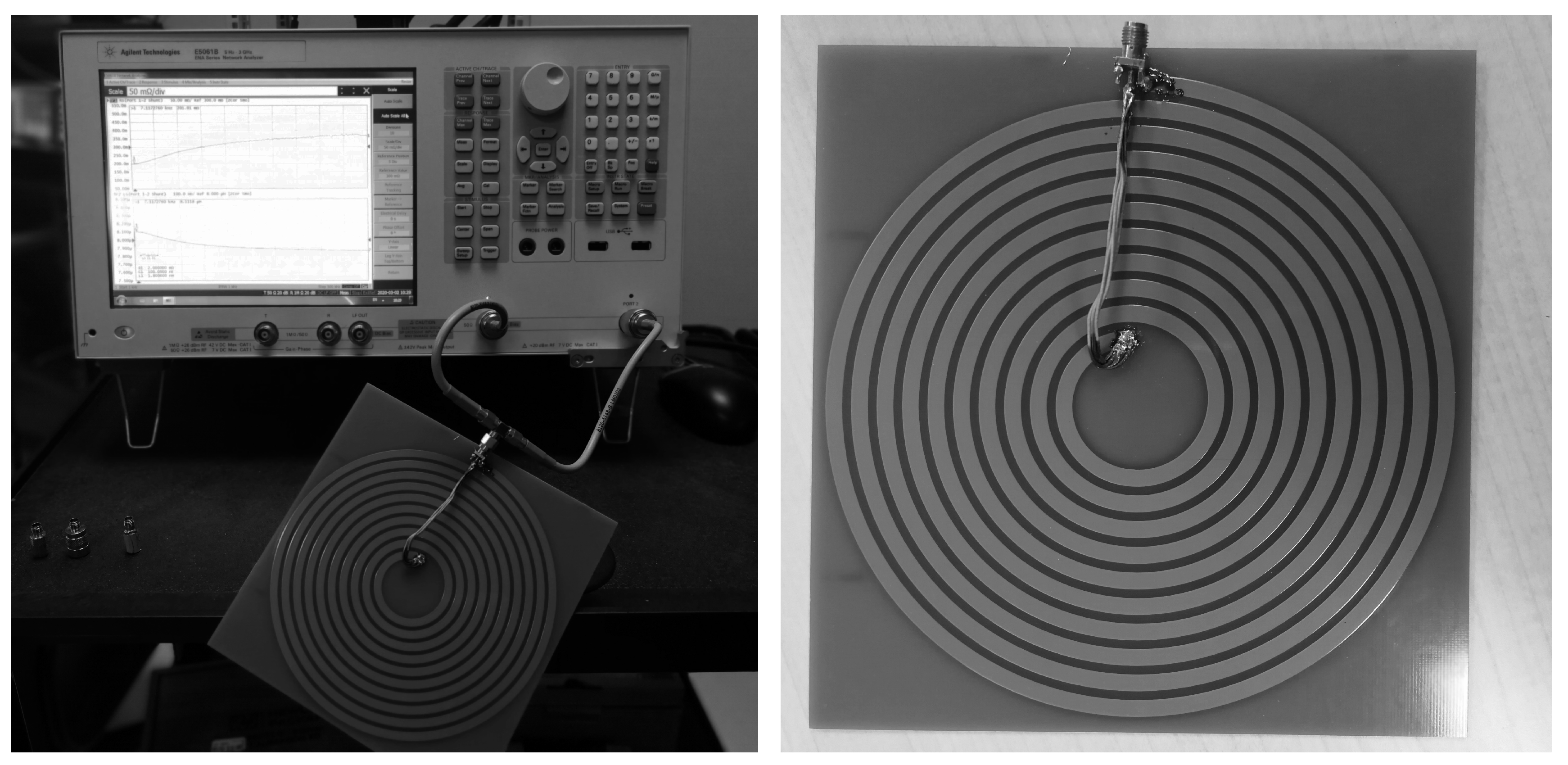
4. AC Resistance Measurements

In this paper, 9 PCB windings were designed and tested in the laboratory to verify the proposed analysis and simulation results. To have a good agreement to the previous simulations, single layer PCB with a copper thickness of 0.070 mm was used and the dimensional parameters are chosen equivalent to the windings used in simulations. All prototypes are divided into 3 groups with 3, 7 and 10 turns and full designed parameters are presented in Table 5. The Agilent vector analyzer (VNA) E5061B is employed to measure the AC resistance of the windings and set up as in Figure 13. In particular, port 1 and 2 of VNA are connected to a splitter by 2 SMA-SMA cables and port 1–2 shunt measurement method is used. The remaining SMA connector is soldered directly to one end of the measured winding, the other end is connected to the SMA connector by 6 parallel litz wires. By doing that, the fixture AC resistance is kept low in the frequency range of interest. Hence, it does not affect the resistance of the winding. To limit the inaccuracy of measurements, the VNA is kept at room temperature during the process and the Open/Short/Broadband Load impedance calibration need to be done before each measurement. The frequency range is set from 200 kHz to 700 kHz, step 1 kHz and the DC resistance is the average value of the resistance in the range 5 kHz to 7 kHz. Winding resistances are directly extracted from the VNA and compared by group with the same number of turns corresponding to studies 1, 2 and 3 in the previous Section while DC resistances of 9 prototypes are shown in Table 6.

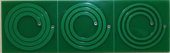
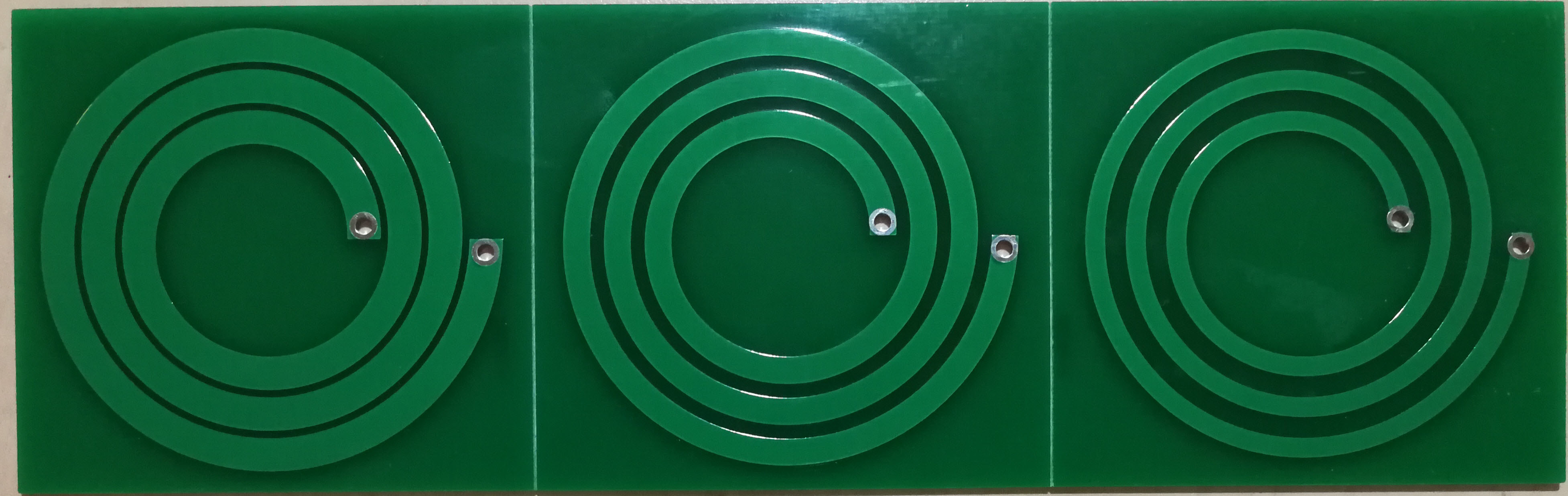
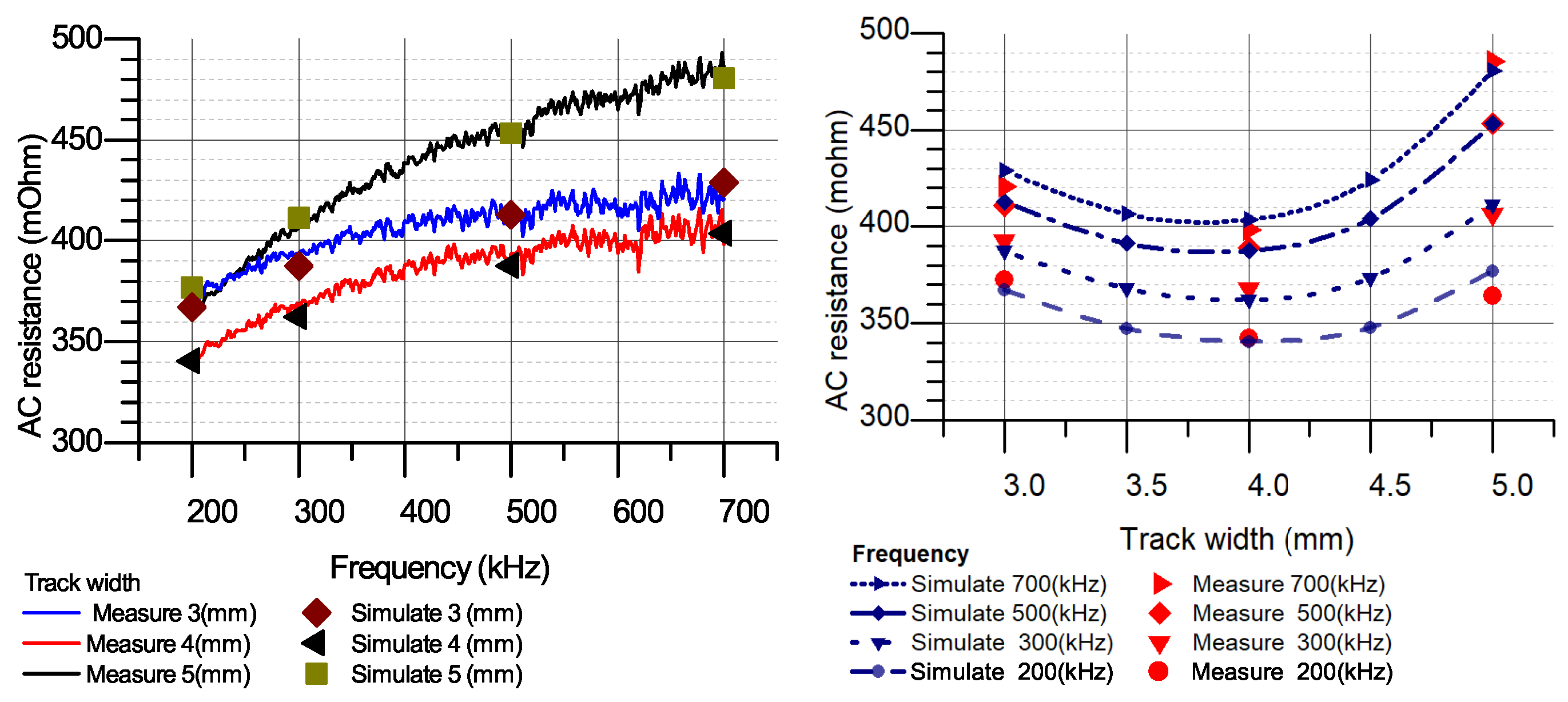
4.1. Group 1: Three-Turn PCB windings

Figure 14 and Figure 15 present the prototypes and AC resistances of 3-Turn windings. Measurement results show that the 5 mm winding has the smallest AC resistance throughout the frequency range from 200 kHz to 700 kHz. At the same time, these measurements have a difference of 1 m Ω to 2 m Ω compared to the simulation results, which corresponds to an error of 5 % . The AC to DC ratios are compared to the optimal line in the Figure 16 and shown that 5 mm winding presents a ratio very close to the optimal line. This result is consistent with computation and simulation results presented in the previous Sections.

4.2. Group 2: Seven-Turn PCB Windings

The results of seven-Turn windings are shown in Figure 17 and Figure 18 including the prototypes and AC resistance measurements. The experimental results are compared to simulations showing the difference under 5 % and the 4.2 mm is the lowest AC resistance winding in the range of frequency 200 kHz to 700 kHz. The AC resistance improvement is most evident at 700 kHz, about 11.5 % , with the AC resistances R A C _ 4.2 mm = 230 m Ω and R A C _ 5 mm = 260 m Ω of the 4.2 mm and 5 mm windings, respectively. The AC to DC ratios are shown in Figure 19 with the difference between the F r _ 4.2 mm and F r _ o p t i m a l lines is about 0.05 to 0.1, which again show the agreement between simulation and experimental results.

4.3. Group 3: Ten-Turn PCB Windings
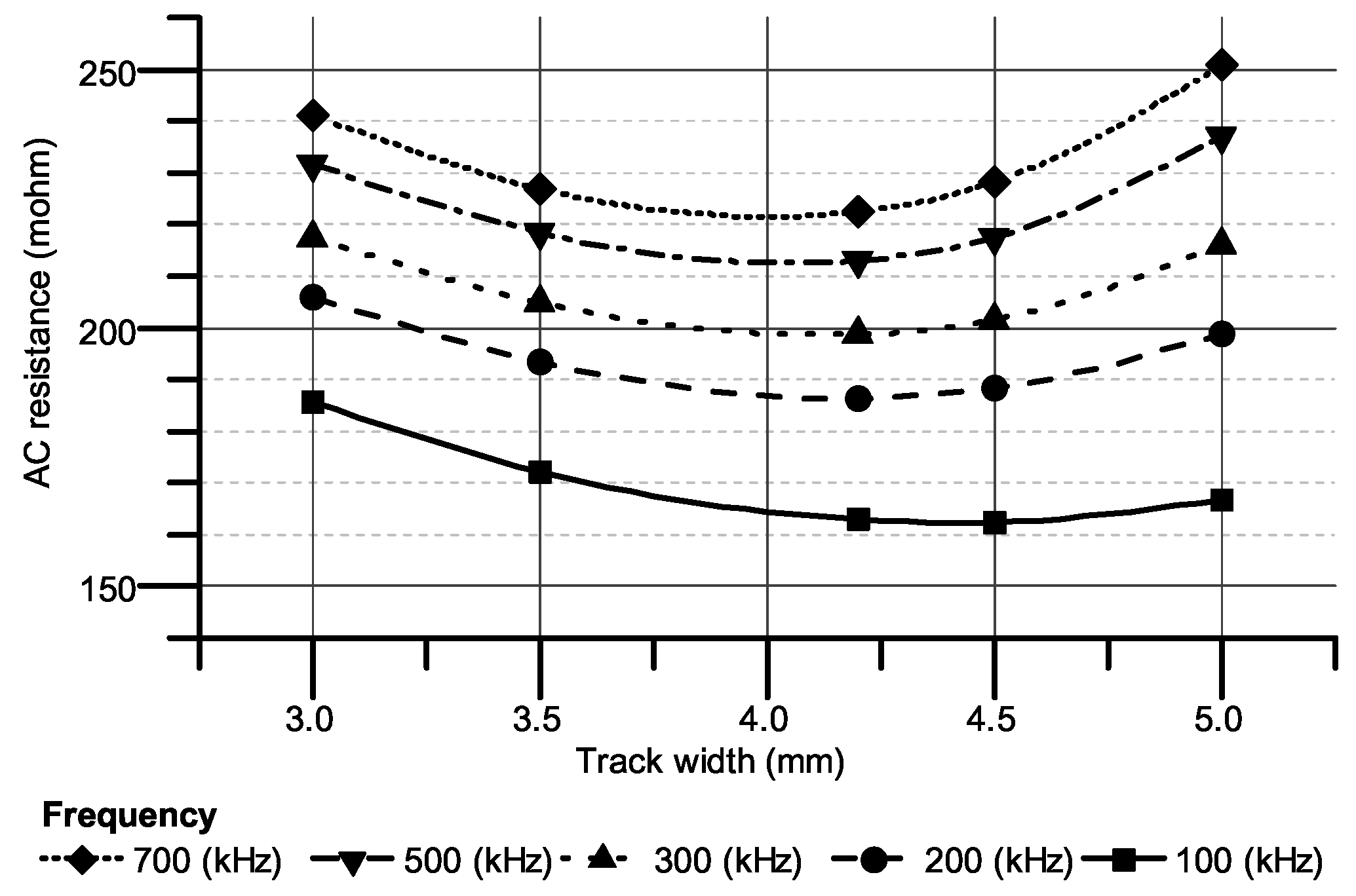
The 10-Turn windings are designed as in Figure 20 and the AC resistances are shown in Figure 21. A similar conclusion with previous two experiments is also drawn when the 4 (mm) winding has the lowest AC resistance. At 700 kHz, the 4 mm and 5 mm windings have AC resistance R A C _ 4 mm = 405 m Ω and R A C _ 5 mm = 485 m Ω , the improvement is about 16.5%. The comparing AC to DC ratios of the 4 mm to the optimal line in Figure 22 shows the compatibility between theory and experimental results. Also, confirming that the 4 mm winding is the optimal design in the group because its ratios have the least differences to the optimal line.
The measured AC to DC ratios of different groups are compared to the optimal values in Table 1 (the blue line) in Figure 23 to prove the correctness of the proposed method. Initially, the F r of maximum allowable track width W = 5 mm of 3 groups are totally different. At 500 kHz, these values are 1.96, 2.58 and 2.71 for 3, 7 and 10-Turn windings, respectively. After adjusting the track width, at optimal designs, the AC to DC ratios of all groups are F r _ 3 T u r n s _ 5 mm = 1.96 , F r _ 7 T u r n s _ 4.2 mm = 1.94 , and F r _ 10 T u r n s _ 4 mm = 1.85 . These results are in accordance with the calculation results F r _ O p t i m a l = 1.89 regardless of number of turns and winding dimension. Moreover, similar results are also recorded in the frequency range from 200 kHz to 700 kHz. Therefore, the 3 groups of windings show a clear explanation about the theory used with 3 achievements:
  • Although initial F r ratios of each group of windings are very different, the optimal track width in each group is also different. However, at optimal points, F r _ o p t i m a l ratios remain unchanged regardless of the number of turns so it can be used as a general standard to optimize AC resistance of PCB winding.
  • The optimal point is not only valid at a specific frequency but a wide range of frequency for different group of windings. Thus, this method is valuable for windings which work in a wide range of frequency.
  • For windings with few turns or windings working in low frequency range, the proximity effect is negligible, therefore, it is not necessary to optimize. The ratio F p r o x i m i t y = ( 1 / 3 ) F s k i n or F r = ( 4 / 3 ) F s k i n can be used as a gap between high and low frequency of a winding.

5. Discussion

Equation (9) points out the relationship between the proximity ratio and track width with an idea that a slight change in track width will cause a significant change of proximity ratio. Consequently, adjusting track width can help to adjust the proximity ratio and the optimal point is achieved when F p r o x i m i t y = ( 1 / 3 ) F s k i n or F r = ( 4 / 3 ) F s k i n . Moreover, the optimal point only varies by F s k i n so it is independent of the number of turns and structure of windings. From the simulation and measurement results, defined W m a x and W o p t i m a l are the maximum allowable and optimal track width of a winding, respectively. A procedure for designing the PCB windings is recommended with a few steps as below:
  • Step 1: The windings need to be designed with the maximum allowable track width W m a x which depends on other parameters like number of turns, required distance between the adjacent turns and dimension of the footprint. Also, the working frequency range needs to be designed from the beginning. After that, the AC to DC ratio at the center frequency is being compared to F s k i n of conductor at this frequency to determine whether the winding need to optimize.
  • Step 2: If F r 4 3 F s k i n , the winding is in optimized condition so no more action need to take place, W o p t i m a l = W m a x .
  • Step 3: If F r > 4 3 F s k i n , the winding need to be optimized by reducing the track width. The F p r o x i m i t y need to be calculated as in Equations (14) and (15):
    F p r o x i m i t y = F r F s k i n
    F p r o x i m i t y _ o p t i m a l = 1 3 F s k i n .
    Finally, the optimal track width W o p t i m a l is drawn according to Equation (9) and Equation (16):
    W o p t i m a l = W max × F p r o x i m i t y _ o p t i m a l F p r o x i m i t y 4 .

6. Conclusions

This paper points out the influence of the skin and proximity effects on AC resistance of a PCB winding. The analysis and simulation results show that by changing the width of the copper track on a fixed footprint, the skin and proximity resistances can be adjusted and the optimal AC resistance is achieved when F p r o x i m i t y is equal to 1 3 F s k i n . The analysis and simulations are verified and the correctness is proved by measurements in the laboratory with three groups of prototypes. The research results show the ability to use the relationship between F p r o x i m i t y and F s k i n as a comparison standard in designing and optimizing spiral winding.

Author Contributions

M.H.N. did the analysis, simulations and verified the results with measurement prototypes. H.F.B. provided supervision and manuscript revised. All authors have read and agreed to the published version of the manuscript.

Funding

This research has been funded by the NSERC under grant number RGPIN 2019-07128.

Conflicts of Interest

The authors declare no conflict of interest.

Abbreviations

The following abbreviations are used in this manuscript:
σ Copper conductivity
δ Copper skin depth
ω Angular frequency
B n External magnetic field
B n Average external magnetic field
EElectric field
FEMFinite element simulation
F s k i n Ratio of AC resistance causes by skin effect to DC resistance
F p r o x i m i t y Ratio of AC resistance causes by proximity effect to DC resistance
F r Ratio of total AC resistance to DC resistance
hTrack thickness
I e d d y Eddy current
I e x Excitation current or main current
J e d d y Eddy current density
LTrack length
PTrack pitch
R A C Total AC resistance causes by skin and proximity effects
R D C DC resistance
R i n Inner radius of a winding
R o u t Outer radius of a winding
R s k i n AC resistance causes by skin effect
R p r o x i m i t y AC resistance causes by proximity effect
VNAVector Network Analyzer Machine
WTrack width
W i n Inner width of a winding
W o u t Outer width of a winding

References

  1. Ropoteanu, C.; Svasta, P.; Ionescu, C. A study of losses in planar transformers with different layer structure. In Proceedings of the 2017 IEEE 23rd International Symposium for Design and Technology in Electronic Packaging (SIITME), Constanta, Romania, 26–29 October 2017; pp. 255–258. [Google Scholar] [CrossRef]
  2. Dai, N.; Lofti, A.W.; Skutt, C.; Tabisz, W.; Lee, F.C. A comparative study of high-frequency, low-profile planar transformer technologies. In Proceedings of the 1994 IEEE Applied Power Electronics Conference and Exposition-ASPEC’94, Orlando, FL, USA, 13–17 February 1994; Volume 1, pp. 226–232. [Google Scholar]
  3. Stadler, A.; Albach, M.; Macary, F. The minimization of copper losses in core-less inductors: Application to foil- and PCB-based planar windings. In Proceedings of the 2005 European Conference on Power Electronics and Applications, Dresden, Germany, 11–14 September 2005. [Google Scholar]
  4. Kim, D.-H.; Park, Y.-J. Calculation of the inductance and AC resistance of planar rectangular coils. Electron. Lett. 2016, 52, 1321–1323. [Google Scholar] [CrossRef]
  5. Serrano, J.; Lope, I.; Acero, J.; Carretero, C.; Burdío, J.M. Mathematical description of PCB-adapted litz wire geometry for automated layout generation of WPT coils. In Proceedings of the IECON 2017-43rd Annual Conference of the IEEE Industrial Electronics Society, Beijing, China, 29 October–1 November 2017. [Google Scholar]
  6. Lope, I.; Acero, J.; Serrano, J.; Carretero, C.; Alonso, R.; Burdio, J.M. Minimization of vias in PCB implementations of planar coils with litz-wire structure. In Proceedings of the 2015 IEEE Applied Power Electronics Conference and Exposition (APEC), Charlotte, NC, USA, 15–19 March 2015. [Google Scholar]
  7. Lope, I.; Carretero, C.; Acero, J.; Burdío, J.M.; Alonso, R. PCB multi-track coils for domestic induction heating applications. In Proceedings of the IECON 2012-38th Annual Conference on IEEE Industrial Electronics Society, Montreal, QC, Canada, 25–28 October 2012. [Google Scholar]
  8. Kutkut, N.H. A simple technique to evaluate winding losses including two-dimensional edge effects. IEEE Trans. Power Electron. 1998, 13, 950–958. [Google Scholar] [CrossRef]
  9. Wang, X.; Wang, L.; Mao, L.; Zhang, Y. Improved Analytical Calculation of High Frequency Winding Losses in Planar Inductors. In Proceedings of the 2018 IEEE Energy Conversion Congress and Exposition (ECCE), Portland, OR, USA, 23–27 September 2018. [Google Scholar]
  10. Antonini, G.; Orlandi, A.; Paul, C.R. Internal impedance of conductors of rectangular cross section. IEEE Trans. Microw. Theory Tech. 1999, 47, 979–985. [Google Scholar] [CrossRef]
  11. Lope, I.; Carretero, C.; Acero, J.; Alonso, R.; Burdío, J.M. AC Power Losses Model for Planar Windings with Rectangular Cross-Sectional Conductors. IEEE Trans. Power Electron. 2013, 29, 23–28. [Google Scholar] [CrossRef]
  12. Su, Y.; Liu, X.; Lee, C.K.; Hui, S.Y. On the relationship of quality factor and hollow winding structure of coreless printed spiral winding (CPSW) inductor. IEEE Trans. Power Electron. 2011, 27, 3050–3056. [Google Scholar]
  13. Meyer, P.; Germano, P.; Perriard, Y. FEM modeling of skin and proximity effects for coreless transformers. In Proceedings of the 2012 15th International Conference on Electrical Machines and Systems (ICEMS), Sapporo, Japan, 21–24 October 2012; pp. 1–6. [Google Scholar]
  14. Rehlaender, P.; Grote, T.; Tikhonov, S.; Niejende, H.; Schafmeister, F.; Böcker, J.; Thiemann, P. A PCB Integrated Winding Using a Litz Structure for a Wireless Charging Coil. In Proceedings of the 2019 21st European Conference on Power Electronics and Applications (EPE ’19 ECCE Europe), Genova, Italy, 3–5 September 2019. [Google Scholar]
  15. Taylor, L.; Margueron, X.; le Menach, Y.; le Moigne, P. Numerical modelling of PCB planar inductors: Impact of 3D modelling on high-frequency copper loss evaluation. IIET Power Electron. 2017, 10, 1966–1974. [Google Scholar] [CrossRef]
  16. Østergaard, C.; Kjeldsen, C.; Nymand, M.; Ramachandran, R. Simulation and measurement of AC resistance for a high power planar inductor design. In Proceedings of the 2019 IEEE 13th International Conference on Compatibility, Power Electronics and Power Engineering (CPE-POWERENG), Sonderborg, Denmark, 23–25 April 2019; pp. 1–5. [Google Scholar] [CrossRef]
  17. Wang, X.; Wang, L.; Mao, L.; Yi, L.; Yang, S. Calculation method of winding loss in high frequency planar transformer. In Proceedings of the 2016 International Conference on Electrical Systems for Aircraft, Railway, Ship Propulsion and Road Vehicles & International Transportation Electrification Conference (ESARS-ITEC), Toulouse, France, 2–4 November 2016; pp. 1–5. [Google Scholar] [CrossRef]
  18. Marian, K. Kazimierczuk, Orthogonality of Skin and Proximity for Individual Foil Layers. In High Frequency Magnetic Components; Wiley: New York, NY, USA, 2014; p. 284. [Google Scholar]
  19. Baliga, B.J. GaN smart power devices and integrated circuits. In Wide Bandgap Semiconductor Power Devices; Woodhead Publishing: Amsterdam, The Netherlands, 2018. [Google Scholar]
  20. Kuhn, W.B.; Ibrahim, N.M. Analysis of current crowding effects in multiturn spiral inductors. IEEE Trans. Microw. Theory Tech. 2001, 49, 31–38. [Google Scholar] [CrossRef] [Green Version]
  21. Qian, G.; Cheng, Y.; Chen, G.; Wang, G. New AC resistance calculation of printed spiral coils for wireless power transfer. In Proceedings of the 2018 19th International Symposium on Quality Electronic Design (ISQED), Santa Clara, CA, USA, 13–14 May 2018. [Google Scholar]
Figure 1. The printed circuit board (PCB) winding inside a planar core.
Electronics 09 00875 g001
Figure 2. A rectangular conductor with its magnetic field.
Electronics 09 00875 g002
Figure 3. The per unit R s k i n of 2 Oz copper track with track width W (left) and inverse track width 1 W (right) simulated by Ansys Maxwel.
Electronics 09 00875 g003
Figure 4. F s k i n of 2 Oz copper track with various track width simulated by Ansys Maxwell.
Electronics 09 00875 g004
Figure 5. The copper track under external field.
Electronics 09 00875 g005
Figure 6. Three-turn W = 5 mm, P = 6 mm PCB winding (left) and W = 3 mm, P = 6 mm (right).
Electronics 09 00875 g006
Figure 7. AC resistances of three-turn PCB windings.
Electronics 09 00875 g007
Figure 8. R A C / R D C of three-turn PCB windings with different track width.
Electronics 09 00875 g008
Figure 9. AC resistances of seven-turn PCB windings.
Electronics 09 00875 g009
Figure 10. R A C / R D C of seven-turn PCB windings with different track widths.
Electronics 09 00875 g010
Figure 11. AC resistances of ten-turn PCB windings.
Electronics 09 00875 g011
Figure 12. R A C / R D C of ten-turn PCB windings with different track width.
Electronics 09 00875 g012
Figure 13. The set up of VNA (left) and a ten-turn spiral winding (right).
Electronics 09 00875 g013
Figure 14. Group-1 prototypes with track width 5 mm (left), 4 mm (middle) and 3 mm (right).
Electronics 09 00875 g014
Figure 15. Group-1 measured and simulated AC resistances with changing in frequency (left) and track width (right).
Electronics 09 00875 g015
Figure 16. Group-1 measured R A C / R D C .
Electronics 09 00875 g016
Figure 17. Group-2 prototypes with track width 5 mm (left), 4.2 mm (middle) and 3 mm (right).
Electronics 09 00875 g017
Figure 18. Group-2 measured and simulated AC resistances with changing in frequency (left) and track width (right).
Electronics 09 00875 g018
Figure 19. Group-2 measured R A C / R D C .
Electronics 09 00875 g019
Figure 20. Group-3 prototypes with track width 5 mm (left), 4 mm (middle) and 3 mm (right).
Electronics 09 00875 g020
Figure 21. Group-3 measured and simulated AC resistances with changing in frequency (left) and track width (right).
Electronics 09 00875 g021
Figure 22. Group-3 measured R A C / R D C .
Electronics 09 00875 g022
Figure 23. Measured F r of 3 group of windings with maximum track width and optimal track width.
Electronics 09 00875 g023
Table 1. The average F s k i n and calculated F r _ o p t i m a l of 2 Oz copper track with the track width varies from 4 mm to 5 mm.
Frequency100 kHz200 kHz300 kHz500 kHz700 kHz
F s k i n 1.151.251.321.411.46
F r _ o p t i m a l 1.531.671.761.891.95
Table 2. Dimensional parameters of three-turn PCB windings.
Profiles/Parameters R in (mm) R out (mm)Number of TurnsPitch (P) (mm)Track Width (W) (mm)
PCB 11533365
PCB 21533364.5
PCB 31533364
PCB 41533363.5
PCB 51533363
Table 3. Dimensional parameters of seven-turn PCB windings.
Profiles/Parameters R in (mm) R out (mm)Number of TurnsPitch (P) (mm)Track Width (W) (mm)
PCB 61557765
PCB 71557764.5
PCB 81557764.2
PCB 91557763.5
PCB 101557763
Table 4. Dimensional parameters of ten-turn PCB windings.
Profiles/Parameters R in (mm) R out (mm)Number of TurnsPitch (P) (mm)Track Width (W) (mm)
PCB 1115751065
PCB 1215751064.5
PCB 1315751064
PCB 1415751063.5
PCB 1515751063
Table 5. Dimensional parameters of PCB prototypes.
GroupParameters/
PCBs
R in
(mm)
R out
(mm)
Number of TurnsPitch (P)
(mm)
Track Width (W)
(mm)
Group 1PCB 11533365
PCB 21533364
PCB 31533363
Group 2PCB 11557765
PCB 21557764.2
PCB 31557763
Group 3PCB 115751065
PCB 215751064
PCB 315751063
Table 6. DC resistances of PCB prototypes.
GroupPCBs R DC measure
(m Ω )
R DC simulate
(m Ω )
Group 1 (Three-Turn PCBs)PCB 126.527.4
PCB 231.533.8
PCB 34144.48
Group 2 (Seven-Turn PCBs)PCB 19394.94
PCB 2111.69104.9
PCB 3154154.59
Group 3 (Ten-Turn PCBs)PCB 1166.86165.41
PCB 2210.6205.315
PCB 3277.5271.84

