Article

A 16 Gbps, Full-Duplex Transceiver over Lossy On-Chip Interconnects in 28 nm CMOS Technology

by
Arash Ebrahimi Jarihani
1,2,*,
Sahar Sarafi
1,
Michael Koeberle
1,
Johannes Sturm
1 and
Andrea M. Tonello
2
1
Department of Engineering & IT, Carinthia University of Applied Sciences, 9524 Villach, Austria
2
Institute of Networked and Embedded Systems, Klagenfurt University, 9020 Klagenfurt, Austria
*
Author to whom correspondence should be addressed.
Electronics 2020, 9(5), 717; https://doi.org/10.3390/electronics9050717
Submission received: 6 April 2020 / Revised: 23 April 2020 / Accepted: 25 April 2020 / Published: 26 April 2020
(This article belongs to the Special Issue Low-Voltage Integrated Circuits Design and Application)

Abstract

:
A high-speed full-duplex transceiver (FDT) over lossy on-chip interconnects is presented. The FDT employs a hybrid circuit to separate the inbound and outbound signals from each other and also performs echo-cancellation with the help of the main and the auxiliary drivers. A hybrid MOS device is utilized for impedance matching and conversion of the received voltage signal into a current signal for amplification. Moreover, a compensation capacitance ( C c ) is used at the output of the main driver to minimize the residual echo signal and achieve a higher data rate. The entire FDT architecture has been designed in TSMC 28 nm CMOS standard process with 0.9 V supply voltage. The performance results validate a 16 Gbps FD operation with a root-mean-square (RMS) jitter of 16.4 ps, and a power efficiency of 0.16 pJ/b/mm over a 5 mm on-chip interconnect without significant effect due to process-voltage-temperature (PVT) variations. To the best knowledge of the authors, this work shows the highest achievable full-duplex data rate, among the solutions reported in the literature to date, yet with low complexity, low layout area of 1581 μ m 2 and competitive power efficiency.

1. Introduction

With recent CMOS technologies, the device sizes are scaled down while the computational speed of the VLSI system is increased. However, the length of the global on-chip interconnects have remained almost the same. Moreover, with the reduction of the width of global interconnects due to scaling, the electrical resistance of the global interconnects got increased. In other words, the on-chip interconnects are RC dominated and very lossy, which decreases the overall bandwidth and the energy-efficiency of the circuitry. Therefore, on-chip interconnects are becoming a power, speed and reliability bottleneck in sub-micron technologies [1] and significantly affect the performance of a network on chip (NoC).
Additional complexity is introduced in on-chip signaling when simultaneous bidirectional, multipoint-to-multipoint and parallel communication is needed. Such interconnects are very common, for example, those used for the on-chip buses to connect different parts of a multi-core processor chip, system on a chip (SoC), and in global address or data-lines for memories. The resistance and delay of interconnects can be reduced by using wider cross-sectional dimensions, however, the area occupied by the interconnect and its capacitance increase, which leads to lower data-rates and higher energy consumption [2,3].
Several unidirectional signaling solutions have been reported to achieve energy-efficient high data rates over on-chip interconnects [4,5,6]. Most of the reported work focuses on the modeling of the interconnects as transmission lines, repeaters, capacitively and resistively driven interconnects, data modulation methods, and current-mode signaling to achieve target specifications [7,8,9,10,11,12,13,14,15,16,17]. For bidirectional data communication, two dedicated unidirectional links may be used. High data rates can be achieved at the cost of increased chip area and power consumption for bidirectional signaling.
In addition to the aforementioned techniques, half-duplex signaling schemes are reported in [18,19,20,21]. This type of signaling allows us to use the same interconnect for both transmitting and receiving the data. Therefore, the effective wire density can be doubled. However, the bandwidth reduces to half due to time-sharing between the transmitting and receiving cycles. The time-sharing problem can be solved if simultaneous bidirectional signaling is used (i.e., full-duplex transmission). FDT is able to transmit and receive data at the same time. Therefore, the required number of interconnections compared to unidirectional signaling schemes decreases.
There are full-duplex transceivers in the literature [22,23,24,25,26,27], which have been extensively explored for off-chip transmission lines in PCBs or cables. Generally, off-chip full-duplex transceivers (FDTs) have high power consumption. Moreover, the behavior and characteristic of on-chip global interconnects are different from the off-chip transmission lines deployed in PCBs, cables and hence, off-chip FDTs are not suitable for on-chip interconnects. Thus, off-chip FDTs cannot be directly used for on-chip interconnects.
Recently, FDTs have been explored for on-chip interconnects [28,29,30,31,32,33]. Initial studies on simultaneous current-mode bidirectional signaling for on-chip interconnection can be found in [28]. In this study, the spice model of a 0.18 μ m CMOS technology solution is used for simulations. The on-chip interconnect is modeled as distributed RC elements. The study shows the power consumption and maximum achievable data rate for various interconnect lengths up to 4.5 mm. However, the overall performance of the proposed circuit is poor. Another current-mode differential bidirectional transceiver with an adaptive impedance matching architecture is presented in [29]. Simulation results using the TSMC 0.18 μ m CMOS process indicate a maximum data rate of 5 Gbps over the on-chip wire of 1 mm with an energy dissipation of 3.8 pJ. Thereinafter, a simultaneous bidirectional transmission scheme has been presented for synchronous data at the two ends of the interconnect achieving a data rate of less than 2 Gbps with increased power consumption [30].
Wary and Mandal [31] provided a detailed analysis of the simultaneous bidirectional signaling. In this current-mode design, transmitting data are phase-shifted and converted to voltage-mode by using a Directional Inverter Buffer (DIB). Then, the modified data is applied to a transconductor circuit performing the weighted addition operation. The signals are converted to current to apply some coefficients for echo cancellation and again voltage modes that may, in turn, increase the uncancelled echo signal, which is critical for simultaneous bidirectional signaling. Nevertheless, the design is complex and a low speed of 4 Gbps (2 Gbps from each side) data-rate is reported. In addition to this, authors in [32] suggest to use a replica based transceiver. Full-duplex data-rate of 10 Gbps is reported, however, the simulation results are at the schematic level. Moreover, a wide channel has been used which is not too much lossy.
Another hybrid circuit topology for simultaneous bidirectional signaling over on-chip interconnects have been proposed in [33]. The designers attempted to mitigate the speed problem by using a MIMO (eight parallel channels and transceivers) structure. Nonetheless, the proposed circuit still has some limitations. Firstly, a short interconnect (3 mm) has been considered. On this interconnect, 2 Gb/s/channel simultaneous bidirectional signaling is reported (16 Gbps in total). Secondly, the eight-bit parallel bus environment occupies a large area without enhancing transmission speed. Thirdly, the energy efficiency of the whole system is limited since 8 parallel structures are used to enhance data-rate.
From the above discussion, it appears evident that there exist still challenges in the realization of high-speed on-chip interconnects. FDT appears a promising approach which however requires careful design to avoid significant self-interference components. In this paper, we propose an alternative FDT architecture that is capable of reaching 16 Gbps transmission using an on-chip interconnect.
In more detail, the major contributions reported in this paper are the following.
A high-speed power-efficient transceiver is proposed for full-duplex signaling over on-chip interconnects. The link utilization is increased by a factor two, thus reducing the link area to half w.r.t. unidirectional transmission. To achieve FDT, a transistor is used as a hybrid device for separating the inbound and outbound signals and performing echo-cancellation with the help of a main and an auxiliary driver. Moreover, the hybrid device employs impedance matching at both ends of the interconnect, which eliminates the necessity of deploying a passive termination for achieving higher bandwidth and therefore higher data-rates.
Finally, the performance of the designed FDT is evaluated by post-layout simulation results using the TSMC 28 nm standard process over a global on-chip interconnect having a typical length of 5 mm [34].
The rest of the paper is organized as follows. Section 2 presents the proposed FDT architecture. Section 3 discusses the circuit design. Section 4 presents the post-layout simulation results followed by the conclusion in Section 5.

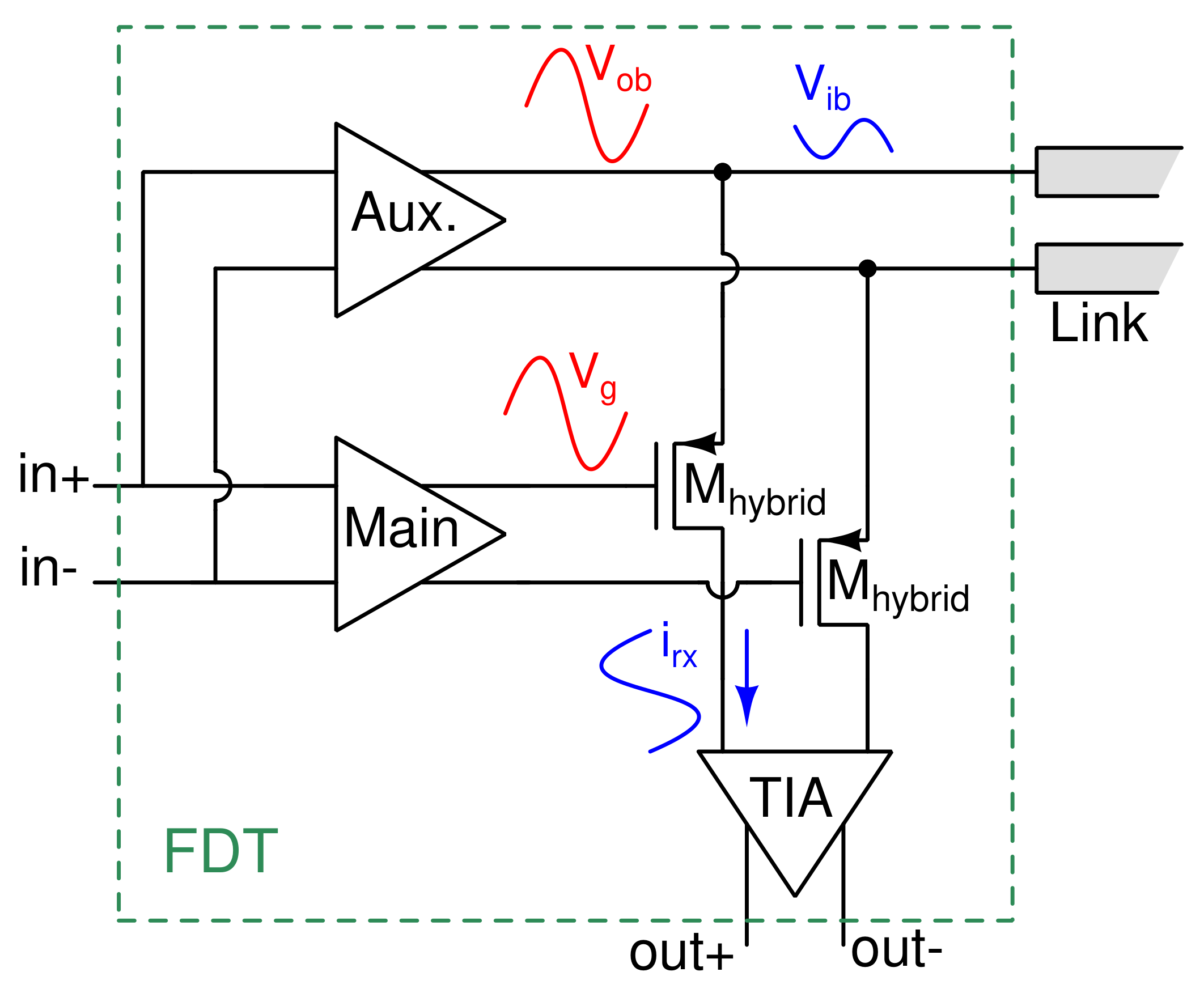
2. Proposed Full-Duplex Transceiver Architecture

Full-duplex transceivers use bidirectional signaling for doubling the data rate. This requires a combination of transmitting and receiving units at both ends of the interconnection. FDT implies the generation of self-interference due to the superposition of the transmitted and received signals. In order to extract the received data from the super-imposed signal, a hybrid structure or echo-cancellation circuitry is required to separate the inbound ( V i b ) and the outbound ( V o b ) signals from each other. Therefore, a new topology with detailed analysis on how to do echo-cancellation and perform simultaneous bidirectional signaling is proposed. A conceptual block diagram of the proposed FDT is shown in Figure 1.
The proposed FDT consists of a main and auxiliary drivers, a hybrid transistor ( M h y b r i d ), and a trans-impedance amplifier (TIA). The hybrid transistor plays an important role to separate the inbound signal from the superimposed signal at the interconnect end.
As known, by virtue of its transconductance ( g m ), M h y b r i d converts changes in its source-gate voltage ( V s g ) to a small-signal drain current [35]. Therefore, by generating the same and equal signals at the gate and the source of the M h y b r i d ( V g = V o b ), no V s g variation comes from the transmitting signal. Consequently, the drain current of the hybrid device is mainly a function of the received signal ( V i b ) from the second transmitter on the other side of the interconnect, which is sensed on V s g . Then, the sensed inbound voltage signal ( V i b ) is converted to the current ( i r x ) by the g m of the hybrid device.
The gate signal ( V g ) of the M h y b r i d is generated by the main driver. However, M h y b r i d operates as a source follower (SF) in the transmitting function of the FDT. Therefore, the generated signal by the main driver at the source of M h y b r i d is V o b , M = α V g , where α = A v ( S F ) < 1. To perform echo-cancellation, the source and the gate voltages of the M h y b r i d must be in-phase and have equal amplitude. For this purpose, an auxiliary driver is employed. It generates the signal V o b , A = β V o b as a function of its steering current and impedance seen by its output. Mathematically, V o b at both end of the interconnect is given by
V o b = V o b , M + V o b , A = α V g + β V o b .
Ideally, α + β should be equal to 1, to perform V o b = V g and have zero echo. As a result, the main and the auxiliary drivers generate the superposition signal V o b altogether. The received signal may contain the unwanted outbound signal V e c h o as uncancelled echo, which is basically due to mismatches between the V o b and V g signals. Finally, the TIA is used to amplify the received current signal ( i r x ) and convert it to voltage to be used by the comparator and data recovery circuitry.

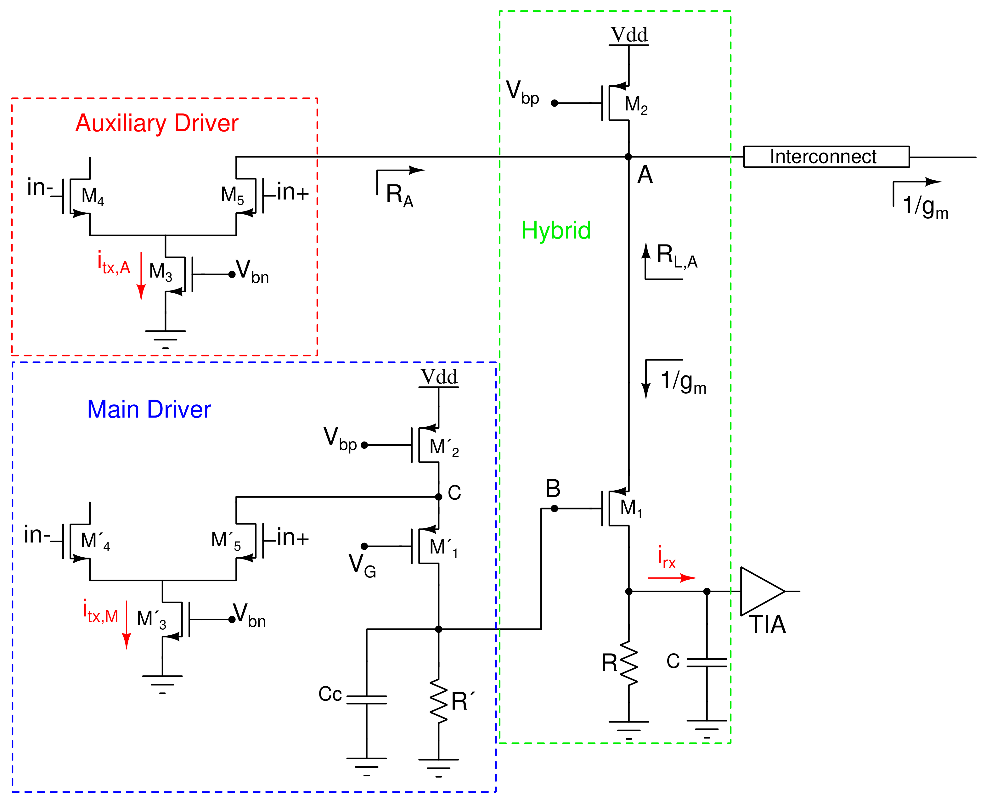
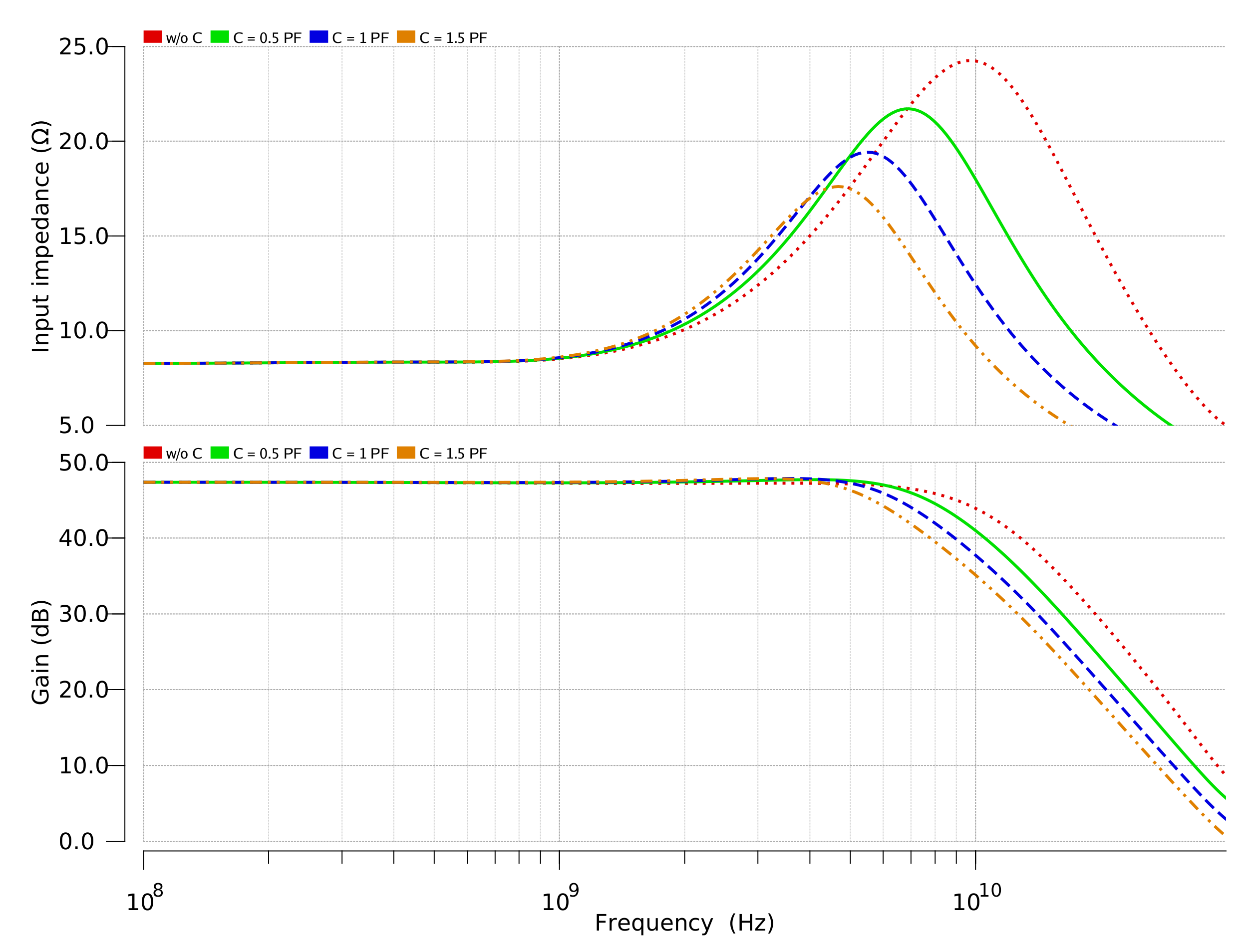
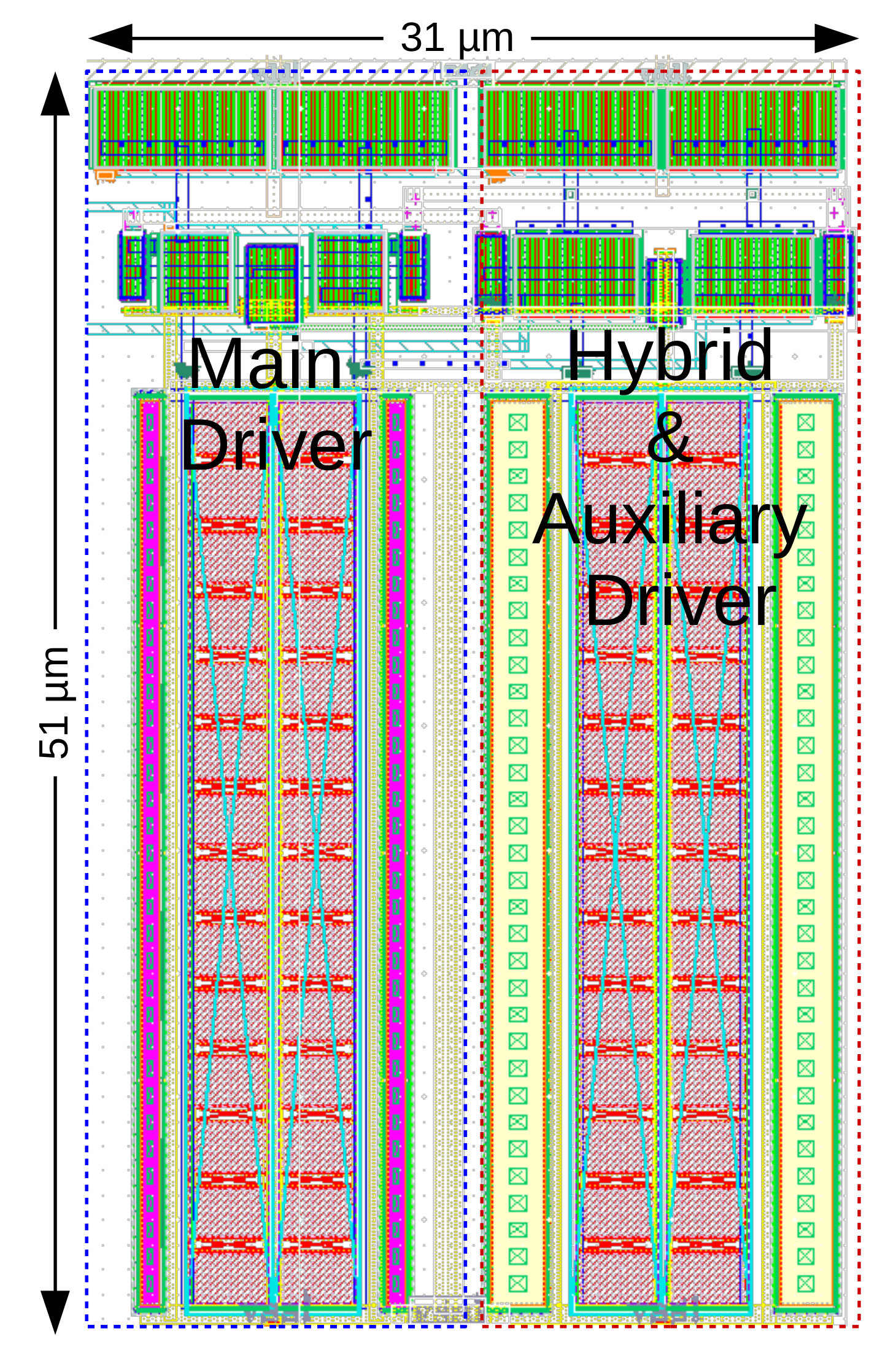
3. Analysis and Circuit Design of the Full-Duplex Transceiver

A transistor-level implementation of the transceiver is shown in Figure 2. To reduce the complexity of the circuit, a single-ended schematic is illustrated. For analysis purposes, the FDT is divided into three parts: hybrid, main and auxiliary drivers.
The major part of the transmitting signal is generated by the main driver. This driver is designed in relation to the hybrid part to have similar process variations.
The portion of the transmitted signal by the main driver ( V o b , M ) can be calculated by the following equations:
A o , M = V g , B i t x , M = [ 1 + ( g m 1 + g m b 1 ) . r o 1 ] . r o 2 . R r o 1 + ( g m 1 + g m b 1 ) . r o 1 . r o 2 + r o 2 + R
α = A v , S F = g m 1 g m 1 + 1 R L , A , w h e r e R L , A = ( R i n t + 1 / g m 1 ) | | r o 2 | | r o 5
V o b , M = α V g , B = A o , M A v , S F i t x , M ,
where V g , B is the gate voltage generated at node B by the main driver, i t x , M is the current steering from the main driver, and R i n t is the resistance of the interconnect.
The auxiliary driver is a simple differential pair, which includes M 3 , M 4 and M 5 devices. Transistors M 4 and M 5 have two operation phases. Based on the pseudo-random binary sequence (PRBS) data that applies to these transistors, they can be ON or OFF. When the transistor is in ON state, it will be operated in a saturation region and leads to a higher output impedance for the driver. Moreover, M 3 is used to adjust the amplitude of the transmitting signal and minimize the uncancelled echo. The minor portion of the transmitting signal which is generated by the auxiliary driver can be expressed as
V o b , A = R A i t x , A , w h e r e R A = 1 / g m 1 | | ( R i n t + 1 / g m 1 ) | | r o 2 .
The hybrid part includes M 1 and M 2 devices and a resistor. While transistor M 1 is the hybrid device, M 2 and resistor (R) are used to bias the hybrid device.
The characteristics of the global on-chip interconnects are different from off-chip transmission lines. For on-chip interconnections, impedance matching with the characteristic impedance ( Z o ) of the interconnect is not necessary. However, the bandwidth of bidirectional signaling can be improved by deploying a low impedance termination at both ends of the interconnect [12]. Therefore, impedance matching is done by matching to the impedance seen from the source of the hybrid device (≈ 1/ g m ).
Matching the signals at nodes A and B for optimum echo-cancellation: The on-chip interconnects are RC dominated. The dominant low-frequency pole at node A can be written as
W p , A = 1 R L , A C A , w h e r e C A = C i n t + C D 2 + C S 1 + C D 5 C i n t .
The capacitance C i n t is approximately 1.05 PF (for the used 5 mm length on-chip interconnect [34]) and total junction capacitances for M 1 , M 2 , and M 5 are approximately 60 fF. Therefore, the influence of the junction capacitances can be neglected at low frequencies.
Likewise, there are two poles at the main driver in nodes C and B, which are related to the internal capacitances of the connected transistors to these nodes. These are high frequency poles ( f 3 d B , C > 40 GHz). However, to have similar signals at nodes A and B and hence lower V e c h o , the capacitive effect of the interconnect should be represented in node B. This can be done by fulfilling the following condition: W p , A = W p , B . Therefore, a compensation capacitance ( C c ) is added to node B to create a dominant low-frequency pole. Thus, the dominant pole at node B is:
W p , B = 1 R B C B , w h e r e R B = r o 1 | | R a n d C B = C c .
With the use of simulations, the magnitude and the phase responses for nodes A and B can be obtained. They are reported in Figure 3. Figure 3a,b show the effect of C c before and after adding it to the main driver output, respectively.
The capacitance C c is added to have not only matched magnitude response but also matched phase response at nodes A and B, which could be a critical issue in time domain echo-cancellation. The compensation capacitance is optimized to have minimum magnitude and phase differences up to 5 GHz. Thus, the structure would be able to support 8 Gbps unidirectional data rate and in turn 16 Gbps full-duplex signaling.
Figure 4 shows that after adding C c , the signal at node A follows the signal at node B with less error during transition (similar rise/fall times).
However, there are some spikes during the transition (switching) time which we refer to as uncancelled echo. These spikes appear in the mid of the received data from the other side due to the transmission line propagation delay. To minimize the peak magnitude of the spikes, the capacitance C is used to realize a filter at the output of the hybrid (TIA input). Figure 5 shows the received current and the effect of C c and C capacitances.
Circuit simulations have been performed for different values of compensation capacitance at the range of ± 30 % . They have shown that the variations in the vertical and horizontal eye openings are less than ± 10 % and ± 5 % , respectively.
After sensing the inbound signal and conversion to current by the hybrid device, a TIA can be used to amplify the received current signal. It should be mentioned that the input impedance and bandwidth of the TIA will be changed due to the use of the capacitance C. Simulations have been implemented to verify the effect of using different values of C and the results are plotted in Figure 6.
The peak value of TIA input impedance and its bandwidth is reduced. However, the variation of input impedance is negligible and the bandwidth ( f 3 d B ) is higher than the required Nyquist frequency for the worst case. Therefore, it does not change the operation of the transceiver at frequencies below 6 GHz and thus the achievable data-rates.

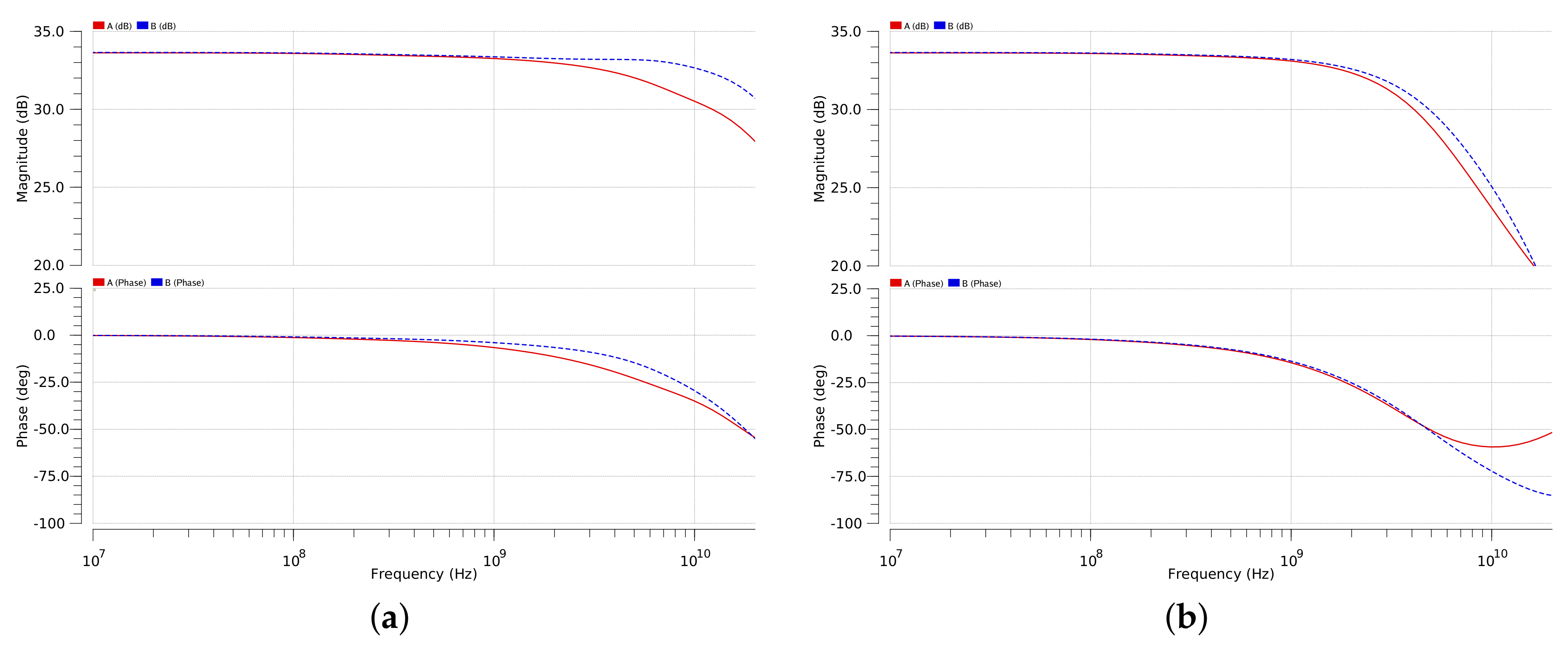
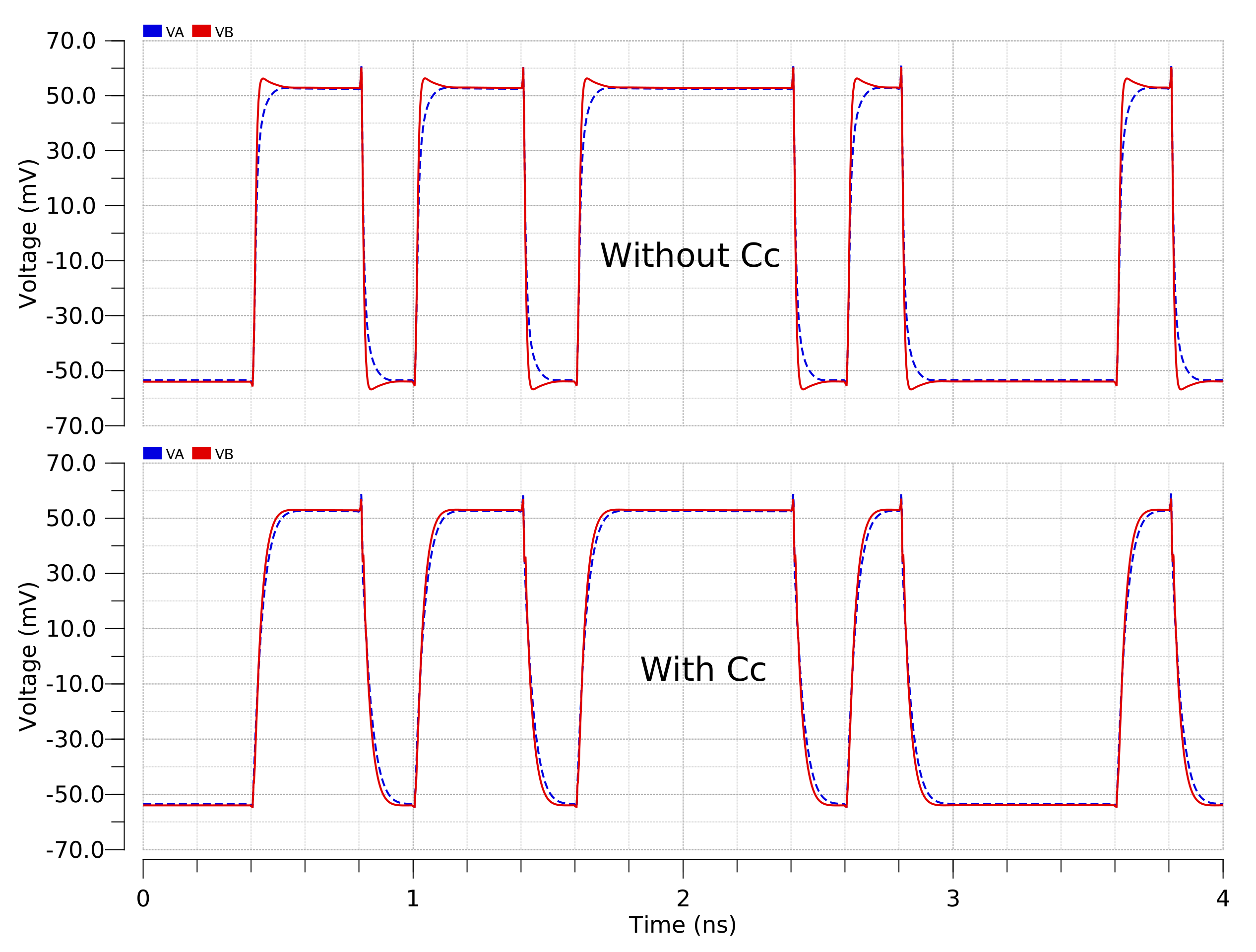
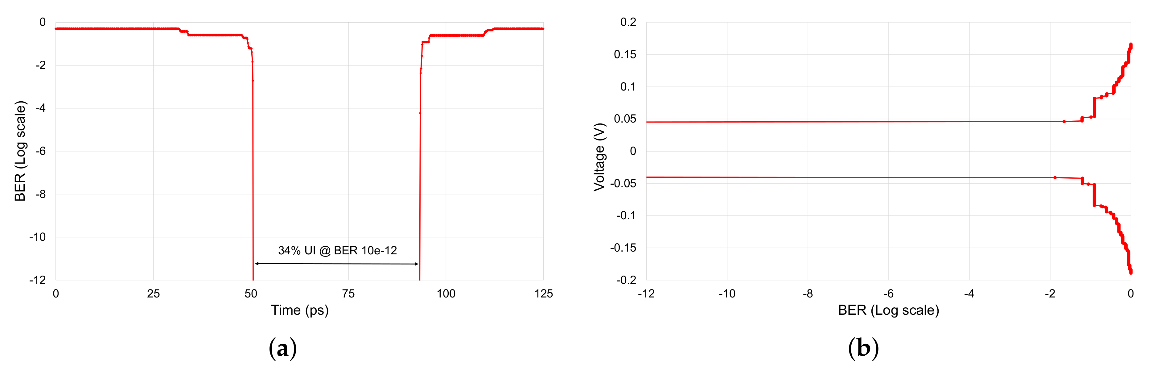
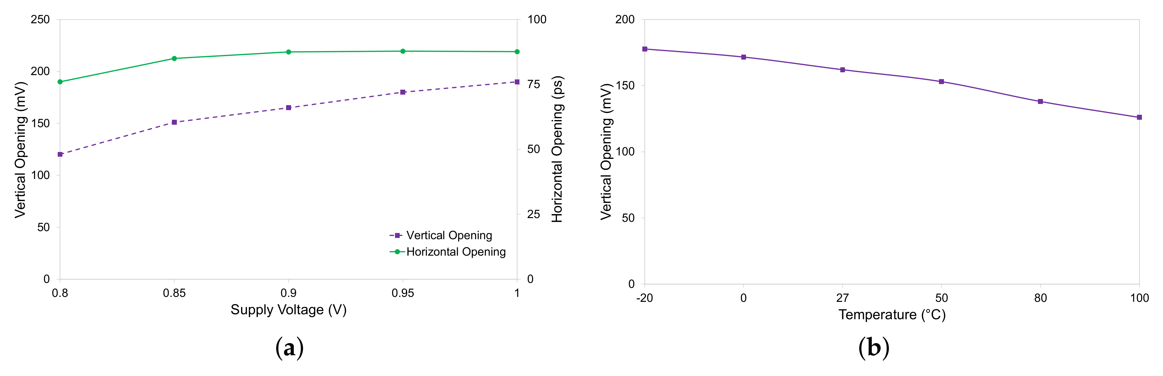
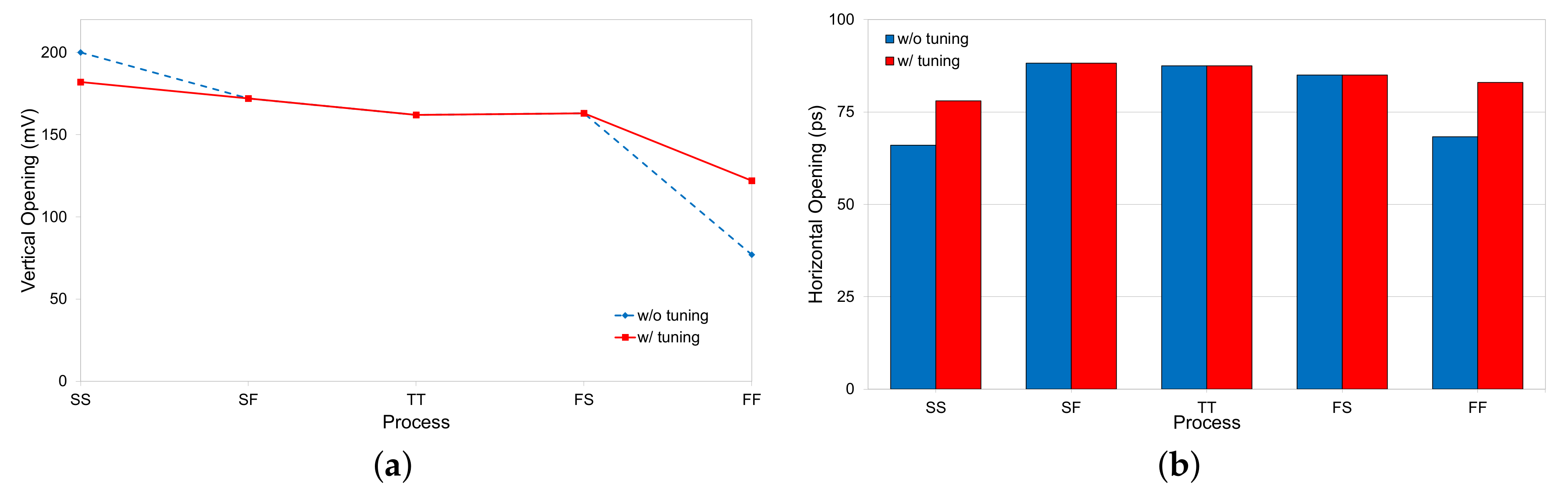
4. Post-Layout Simulation Performance

In this section, the most important performance indicators for the proposed on-chip full-duplex transceiver (e.g., eye-opening, BER, power consumption, robustness against the PVT variations and corner simulations) are analyzed. For this purpose, circuit design for the proposed system has been realized. Figure 7 shows the layout screenshot of the FDT operating at 16 Gbps data rate, which occupies an area of 51 μ m × 31 μ m. In order to verify the performance of the proposed FDT, the post-layout simulations have been performed in 28 nm TSMC CMOS process. The functionality of the FDT is validated over an on-chip interconnect with a length of 5 mm [34]. The link has a width of 0.6 μ m and a spacing of 1 μ m with the adjacent shield layers.
For this purpose, 2 7 1 random bit patterns have been generated using an on-chip PRBS generator [36] and sent to the drivers. The full-duplex operation of the transceiver is realized by transmitting the data streams from the FDT’s at both ends of the interconnect. As a result, a maximum data-rate of 16 Gbps is achieved (8 Gbps from each side with a bit period equal to 125 ps). The differential voltage eye diagrams of the received data are shown in Figure 8 for half-duplex and full-duplex signaling modes.
The plotted eye (full-duplex) has vertical and horizontal openings of 168 mV and 87 ps, respectively. The peak-to-peak and RMS jitter of the eyes for both transceivers are approximately 38.6 and 16.4 ps, respectively. The computed power consumption for each transceiver at 0.9 V supply voltage is 8.827 mW. Therefore, the FDT has a power efficiency of 0.11 pJ/b/mm (0.16 pJ/b/mm including TIA).
In addition, the bit error rate (BER) performance has also been evaluated. Figure 9 shows the BER (in log scale) bathtub curves at 16 Gpbs full-duplex operation. The corresponding timing bathtub curve has 0.34 UI at BER of 10 12 .
The unwanted echo signal can increase because of the mismatches between the main and the auxiliary drivers due to the process-voltage-temperature (PVT) variations. Therefore, to assess the effect, PVT variations are introduced to the FDT at 2×8 Gbps FD operation. The variation in both the vertical and the horizontal eye-opening is observed by changing the supply voltage from 0.8 to 1 V. As can be seen from Figure 10, the vertical eye opening decreases by decreasing the supply voltage and vice versa. By lowering the supply voltage to 0.8 V, the horizontal eye opening decreases approximately 11% only. Moreover, the performance of the FDT is validated while the temperature variations are applied. By increasing the temperature from room temperature to 100 °C and lowering to −20 °C, the eye-opening decreases by 22% and increases by 9%, respectively. However, the horizontal opening remains almost constant for the whole range from −20 °C to 100 °C.
The variations of vertical and horizontal eye openings for different process corners are plotted in Figure 11. The worst-case performances occur in slow-slow (SS) and fast-fast (FF) corners. Nevertheless, the eye in these corners is open enough allowing reliable data detection. It should be mentioned that the mismatch between the voltage swings at nodes A and B due to the process variation at SS and FF corners can be compensated by tuning the current of the auxiliary driver. Therefore, the echo voltage is minimized and the eye-opening is maximized.
Finally, a synthetic comparison of the proposed system with the on-chip full-duplex transceivers reported in the literature is summarized in the Table 1. Some details about these solutions have been given in the introduction. The comparison is made in terms of technology size, supply voltage, interconnect length, offered data rate, energy efficiency, and area occupied. The results show that the proposed solution can offer the highest data rate of 16 Gbps among the other designs with competitive power consumption. The solution described in [32] has better energy efficiency. However, the offered data rate is lower and equal to 10 Gbps. Looking at the design reported in [29] and its achieved data rate, it is expected that this will be affected negatively, if longer on-chip interconnects are used. As an overall result, the proposed FDT solution has a much better overall performance in comparison with the state-of-the-art.

5. Conclusions

In this paper, a high-speed full-duplex transceiver for simultaneously transmitting and receiving data across an on-chip interconnect is presented. A hybrid device is utilized to separate the inbound and the outbound signals from each other and perform echo-cancellation by the combination of the main and the auxiliary drivers. Moreover, the hybrid transistor is used as an active low impedance termination which helps to improve the overall bandwidth of the transceiver. The proposed FDT architecture has been designed in 28 nm, 0.9 V CMOS process. The transceiver has a power efficiency of 0.16 pJ/b/mm for a data rate of 16 Gbps while performing simultaneous bidirectional transmission. The transceiver performance has been assessed through post-layout simulation as a function of process parameters, voltage and temperature variations. It is robust to the introduced PVT variations in the echo cancellation. The post-layout simulations have been carried out over a 5 mm length on-chip interconnect to evaluate the performance of the transceiver.

Author Contributions

Conceptualization, A.E.J.; methodology, A.E.J.; software, A.E.J.; validation, A.E.J. and S.S.; investigation, A.E.J.; writing—original draft preparation, A.E.J.; writing—review and editing, A.E.J., S.S., M.K., and A.M.T.; supervision, J.S. and A.M.T.; project administration, M.K. All authors have read and agreed to the published version of the manuscript.

Funding

This research is funded by the Austrian Research Promotion Agency (FFG) under the Ideation project.

Acknowledgments

The authors would like to thank the Infineon Technologies Austria AG for their support.

Conflicts of Interest

The authors declare no conflict of interest.

References

  1. Banerjee, K.; Souri, S.J.; Kapur, P.; Saraswat, K.C. 3-D ICs: A Novel Chip Design for Improving Deep-Submicrometer Interconnect Performance and Systems-on-Chip Integration. Proc. IEEE 2001, 89, 602–633. [Google Scholar] [CrossRef] [Green Version]
  2. Davis, J.A.; Venkatesan, R.; Kaloyeros, A.; Beylansky, M.; Souri, S.J.; Banerjee, K.; Saraswat, K.C.; Rahman, A.; Reif, R.; Meindl, J. Interconnect Limits on Gigascale Integration (GSI) in the 21st Century. Proc. IEEE 2001, 89, 305–324. [Google Scholar] [CrossRef] [Green Version]
  3. Naeemi, A.; Sarvari, R.; Memdl, J. On-Chip Interconnect Networks at the End of the Roadmap: Limits and Nanotechnology Opportunities. In Proceedings of the 2006 International Interconnect Technology Conference, Burlingame, CA, USA, 5–7 June 2006; pp. 201–203. [Google Scholar] [CrossRef]
  4. Zhang, L.; Zhang, Y.; Chen, H.; Yao, B.; Hamilton, K.; Cheng, C.-K. On-Chip Interconnect Analysis of Performance and Energy Metrics Under Different Design Goals. IEEE Trans. Very Large Scale Integr. VLSI Syst. 2011, 19, 520–524. [Google Scholar] [CrossRef]
  5. Zhang, L.; Zhang, Y.; Tsuchiya, A.; Hashimoto, M.; Kuh, E.S.; Cheng, C.-K. High Performance on-Chip Differential Signaling Using Passive Compensation for Global Communication. In Proceedings of the 2009 Asia and South Pacific Design Automation Conference, Yokohama, Japan, 19–22 January 2009; pp. 385–390.
  6. Weng, S.-H.; Zhang, Y.; Buckwalter, J.F.; Cheng, C.-K. Energy Efficiency Optimization Through Codesign of the Transmitter and Receiver in High-Speed On-Chip Interconnects. IEEE Trans. Very Large Scale Integr. VLSI Syst. 2014, 22, 938–942. [Google Scholar] [CrossRef]
  7. Bai, X.; Zhao, J.; Zuo, S.; Zhou, Y. A 2.5 Gbps, 10-Lane, Low-Power, LVDS Transceiver in 28 nm CMOS Technology. Electronics 2019, 8, 350. [Google Scholar] [CrossRef] [Green Version]
  8. Chang, R.T.; Talwalkar, N.; Yue, C.P.; Wong, S.S. Near Speed-of-Light Signaling over on-Chip Electrical Interconnects. IEEE J. Solid-State Circuits 2003, 38, 834–838. [Google Scholar] [CrossRef] [Green Version]
  9. Jose, A.P.; Shepard, K.L. Distributed Loss-Compensation Techniques for Energy-Efficient Low-Latency On-Chip Communication. IEEE J. Solid-State Circuits 2007, 42, 1415–1424. [Google Scholar] [CrossRef]
  10. Lee, S.-H.; Lee, S.-K.; Kim, B.; Park, H.-J.; Sim, J.-Y. Current-Mode Transceiver for Silicon Interposer Channel. IEEE J. Solid-State Circuits 2014, 49, 2044–2053. [Google Scholar] [CrossRef]
  11. Dobkin, R.; Moyal, M.; Kolodny, A.; Ginosar, R. Asynchronous Current Mode Serial Communication. IEEE Trans. Very Large Scale Integr. VLSI Syst. 2010, 18, 1107–1117. [Google Scholar] [CrossRef] [Green Version]
  12. Kim, B.; Stojanovic, V. An Energy-Efficient Equalized Transceiver for RC-Dominant Channels. IEEE J. Solid-State Circuits 2010, 45, 1186–1197. [Google Scholar] [CrossRef]
  13. Wary, N.; Mandal, P. A Low Impedance Receiver for Power Efficient Current Mode Signaling across on-Chip Global Interconnects. AEU Int. J. Electron. Commun. 2014, 68, 969–975. [Google Scholar] [CrossRef]
  14. Lee, J.; Lee, W.; Cho, S. A 2.5-Gb/s On-Chip Interconnect Transceiver With Crosstalk and ISI Equalizer in 130 Nm CMOS. IEEE Trans. Circuits Syst. Regul. Pap. 2012, 59, 124–136. [Google Scholar] [CrossRef]
  15. Schinkel, D.; Mensink, E.; Klumperink, E.A.M.; van Tuijl, E.; Nauta, B. Low-Power, High-Speed Transceivers for Network-on-Chip Communication. IEEE Trans. Very Large Scale Integr. VLSI Syst. 2009, 17, 12–21. [Google Scholar] [CrossRef]
  16. Hoppner, S.; Walter, D.; Hocker, T.; Henker, S.; Hanzsche, S.; Sausner, D.; Ellguth, G.; Schlussler, J.-U.; Eisenreich, H.; Schuffny, R. An Energy Efficient Multi-Gbit/s NoC Transceiver Architecture With Combined AC/DC Drivers and Stoppable Clocking in 65 Nm and 28 Nm CMOS. IEEE J. Solid-State Circuits 2015, 50, 749–762. [Google Scholar] [CrossRef]
  17. Gaggatur, J.S.; Thulasiraman, D. A Power Efficient Active Inductor-Based Receiver Front End for 20 Gb/s High Speed Serial Link. AEU Int. J. Electron. Commun. 2019, 111, 152886. [Google Scholar] [CrossRef]
  18. Chowdhury, A.R.; Wary, N.; Mandal, P. Energy Efficient Bidirectional Equalized Transceiver with PVT Insensitive Active Termination. In Proceedings of the 2019 32nd International Conference on VLSI Design and 2019 18th International Conference on Embedded Systems (VLSID), Delhi, India, 5–9 January 2019; pp. 25–30. [Google Scholar]
  19. Ito, H.; Kimura, M.; Miyashita, K.; Ishii, T.; Okada, K.; Masu, K. A Bidirectional- and Multi-Drop-Transmission-Line Interconnect for Multipoint-to-Multipoint On-Chip Communications. IEEE J. Solid-State Circuits 2008, 43, 1020–1029. [Google Scholar] [CrossRef]
  20. Dave, M.; Satkuri, R.; Jain, M.; Shojaei, M.; Sharma, D. Low-Power Current-Mode Transceiver for on-Chip Bidirectional Buses. In Proceedings of the 2010 ACM/IEEE International Symposium on Low-Power Electronics and Design (ISLPED), Austin, TX, USA, 18–20 August 2010; pp. 61–66. [Google Scholar]
  21. Wary, N.; Mandal, P. High-Speed Energy-Efficient Bi-Directional Transceiver for on-Chip Global Interconnects. IET Circuits Devices Syst. 2015, 9, 319–327. [Google Scholar] [CrossRef]
  22. Yeung, E.; Horowitz, M.A. A 2.4 Gb/s/Pin Simultaneous Bidirectional Parallel Link with per-Pin Skew Compensation. IEEE J. Solid-State Circuits 2000, 35, 1619–1628. [Google Scholar] [CrossRef] [Green Version]
  23. Tomita, Y.; Tamura, H.; Kibune, M.; Ogawa, J.; Gotoh, K.; Kuroda, T. A 20-Gb/s Simultaneous Bidirectional Transceiver Using a Resistor-Transconductor Hybrid in 0.11-μm CMOS. IEEE J. Solid-State Circuits 2007, 42, 627–636. [Google Scholar] [CrossRef]
  24. Drost, R.J.; Wooley, B.A. An 8-Gb/s/Pin Simultaneously Bidirectional Transceiver in 0.35-μm CMOS. IEEE J. Solid-State Circuits 2004, 39, 1894–1908. [Google Scholar] [CrossRef]
  25. Casper, B.; Martin, A.; Jaussi, J.E.; Kennedy, J.; Mooney, R. An 8-Gb/s Simultaneous Bidirectional Link with on-Die Waveform Capture. IEEE J. Solid-State Circuits 2003, 38, 2111–2120. [Google Scholar] [CrossRef]
  26. Tamura, H.; Kibune, M.; Takahashi, Y.; Doi, Y.; Chiba, T.; Higashi, H.; Takauchi, H.; Ishida, H.; Gotoh, K. 5 Gb/s Bidirectional Balanced-Line Link Compliant with Plesiochronous Clocking. In Proceedings of the 2001 IEEE International Solid-State Circuits Conference, Digest of Technical Papers, ISSCC (Cat. No.01CH37177), San Francisco, CA, USA, 7 February 2001; pp. 64–65. [Google Scholar]
  27. Rao, P.V.S.; Mandal, P. Current-Mode Full-Duplex (CMFD) Signaling for High-Speed Chip-to-Chip Interconnect. Microelectron. J. 2011, 42, 957–965. [Google Scholar]
  28. Huang, H.-Y.; Wu, C.-C.; Chen, S.-L. Simultaneous Current-Mode Bidirectional Signaling for on-Chip Interconnection. In Proceedings of the 2004 IEEE Asia-Pacific Conference on Advanced System Integrated Circuits, Fukuoka, Japan, 5 August 2004; pp. 380–383. [Google Scholar]
  29. Huang, H.-Y.; Pu, R.-I.; Lee, M.-T. Simultaneous Bidirectional Transceiver with Impedance Matching. In Proceedings of the 2008 15th IEEE International Conference on Electronics, Circuits and Systems, St. Julien’s, Malta, 31 August–3 September 2008; pp. 312–315. [Google Scholar]
  30. Huang, H.-Y.; Pu, R.-I. Differential Bidirectional Transceiver for on-Chip Long Wires. Microelectron. J. 2011, 42, 1208–1215. [Google Scholar] [CrossRef]
  31. Wary, N.; Mandal, P. Current-Mode Full-Duplex Transceiver for Lossy On-Chip Global Interconnects. IEEE J. Solid-State Circuits 2017, 52, 2026–2037. [Google Scholar] [CrossRef]
  32. Wary, N.; Mandal, P. Current-Mode Simultaneous Bidirectional Transceiver for on-Chip Global Interconnects. In Proceedings of the 2015 6th Asia Symposium on Quality Electronic Design (ASQED), Kula Lumpur, Malaysia, 4–5 August 2015; pp. 19–24. [Google Scholar]
  33. Duvvuri, D.; Agarwal, S.; Pasupureddi, V.S.R. A New Hybrid Circuit Topology for Simultaneous Bidirectional Signaling over on-Chip Interconnects. In Proceedings of the 2016 IEEE International Symposium on Circuits and Systems (ISCAS), Montreal, QC, Canada, 22–25 May 2016; pp. 2342–2345. [Google Scholar]
  34. Jarihani, A.E.; Sarafi, S.; Koberle, M.; Sturm, J.; Tonello, A.M. Characterization of On-Chip Interconnects: Case Study in 28 Nm CMOS Technology. In Proceedings of the 2019 Austrochip Workshop on Microelectronics (Austrochip), Vienna, Austria, 24 October 2019; pp. 93–99. [Google Scholar]
  35. Razavi, B. Design of Analog CMOS Integrated Circuits; McGraw-Hill: New York, NY, USA, 2001. [Google Scholar]
  36. Bodha, R.R.R.; Sarafi, S.; Kale, A.; Koberle, M.; Sturm, J. A Half-Rate Built-In Self-Test for High-Speed Serial Interface Using a PRBS Generator and Checker. In Proceedings of the 2019 Austrochip Workshop on Microelectronics (Austrochip), Vienna, Austria, 24 October 2019; pp. 43–46. [Google Scholar]
Figure 1. Architecture of the proposed full-duplex transceiver.
Electronics 09 00717 g001
Figure 2. Schematic of the full-duplex transceiver.
Electronics 09 00717 g002
Figure 3. Magnitude and phase responses at nodes A and B: (a) before and (b) after adding C c .
Electronics 09 00717 g003
Figure 4. Transient signals at nodes A and B, before and after adding Cc.
Electronics 09 00717 g004
Figure 5. Received current before and after adding Cc and C capacitances.
Electronics 09 00717 g005
Figure 6. Trans-impedance amplifier (TIA) input impedance and output bandwidth for different C values.
Electronics 09 00717 g006
Figure 7. Layout of the full-duplex transceiver.
Electronics 09 00717 g007
Figure 8. (a) Half-duplex signaling of 8 Gbps and (b) full-duplex data transmission (16 Gbps) of the received signal.
Electronics 09 00717 g008
Figure 9. (a) Horizontal and (b) Vertical bathtub curves for full-duplex signaling of 16 Gbps.
Electronics 09 00717 g009
Figure 10. Variation of eye opening with: (a) supply voltage and (b) temperature variations.
Electronics 09 00717 g010
Figure 11. (a) Vertical and (b) Horizontal opening of the eye at different process cornes with and without tuning the auxiliary driver at worst corners.
Electronics 09 00717 g011
Table 1. Comparison of the proposed full-duplex transceiver with recent literature.
Ref.[29] *[30] # [31] # [32] *[33] *This work **
Technology (nm)180180180656528
Supply Voltage (V)N/A1.81.811.10.9
Interconnect Length (mm)1 mm5 mm5 mm5 mm3 mm5 mm
Data Rate (Gbps)50.92410216
Energy Efficiency (pJ/b)3.89.480.950.381.540.8
Area ( μ m 2 )-42001275-13641581
*: Schematic Simulated results; **: Post-layout Simulated results; #: Measured results.

