A 2.4 GHz 2.9 mW Zigbee RF Receiver with Current-Reusing and Function-Reused Mixing Techniques


Abstract
:1. Introduction
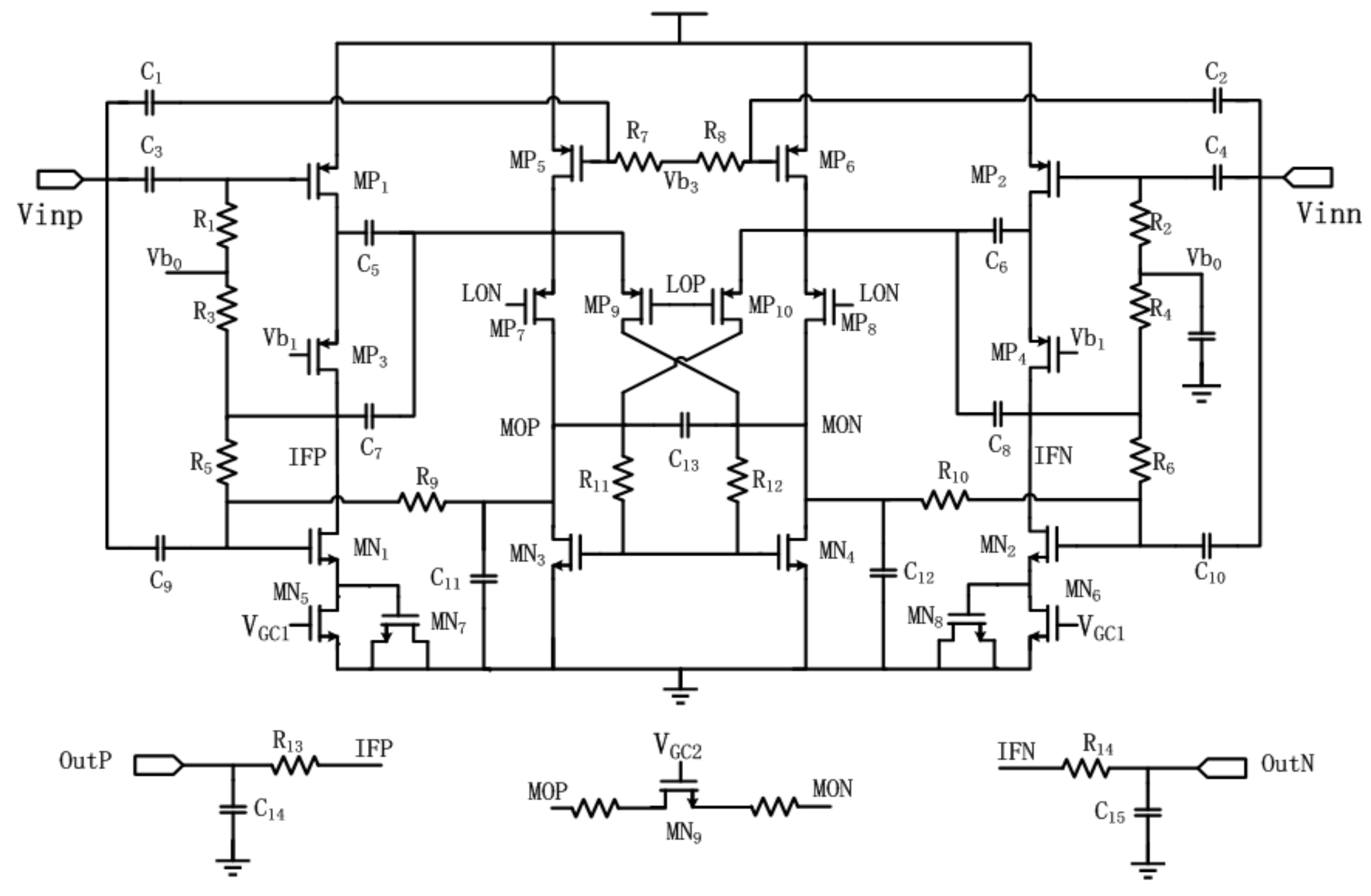
2. Circuit Design
2.1. The Current-Reusing Structure
2.2. The Function-Reused Mixer
2.3. The IF Modules
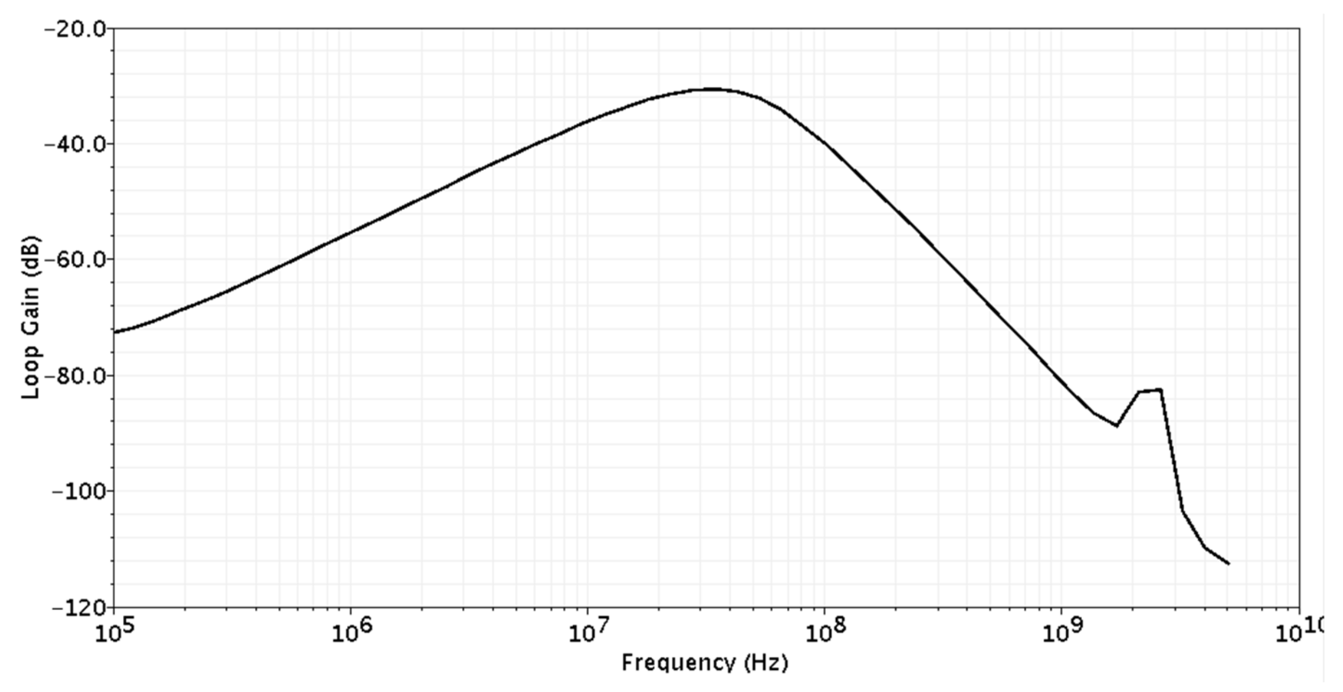
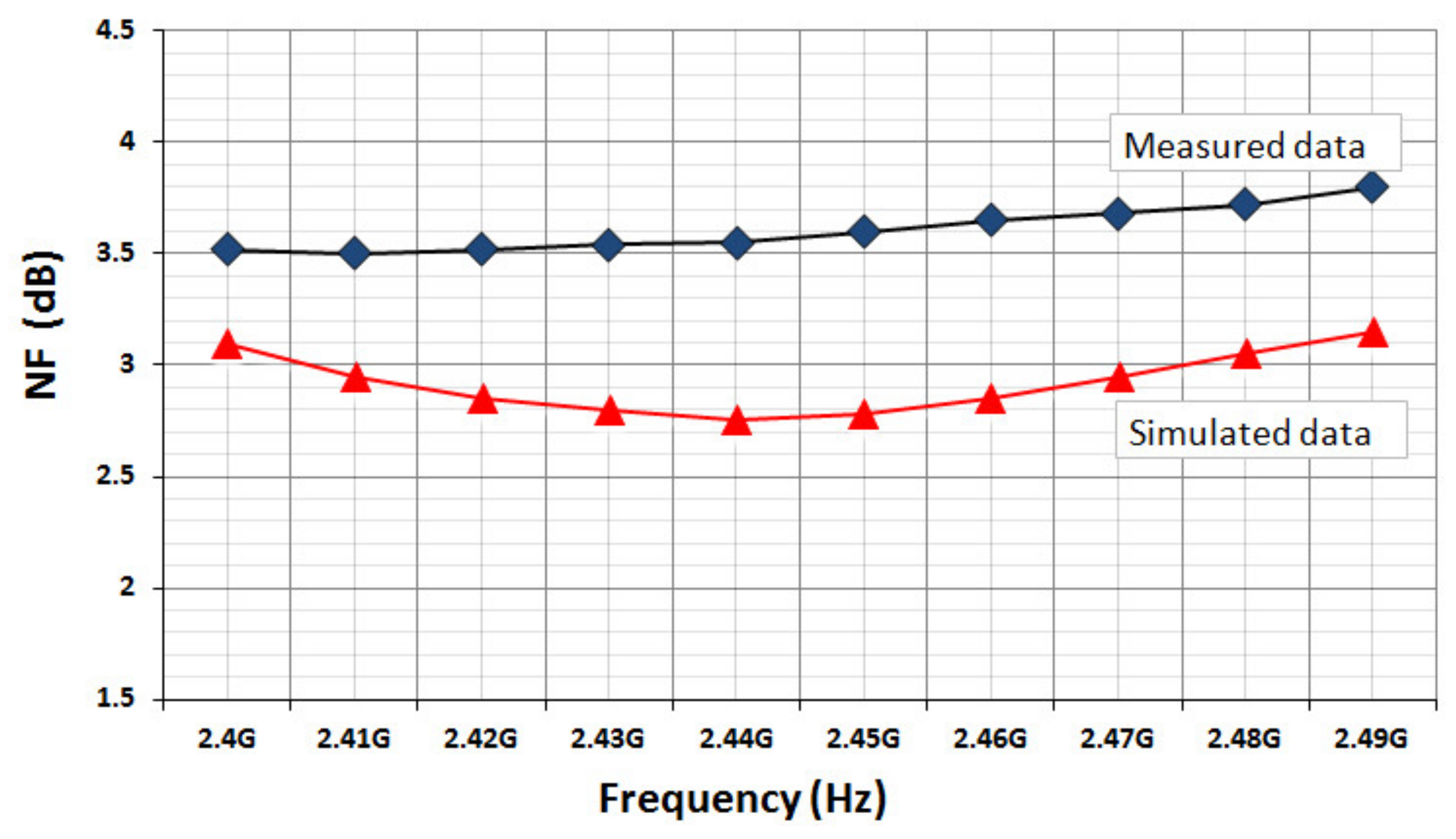
3. Experimental Results
4. Conclusions
Author Contributions
Funding
Conflicts of Interest
References
- Larson, L. RF and microwave hardware challenges for future radio spectrum access. Proc. IEEE 2014, 102, 321–333. [Google Scholar] [CrossRef]
- Liscidini, A.; Mazzanti, A.; Tonietto, R.; Vandi, L.; Andreani, P.; Castello, R. Single-Stage low-power quadrature RF receiver front-end: The LMV cell. IEEE J. Solid State Circuits 2006, 41, 2832–2841. [Google Scholar] [CrossRef]
- Ghosh, D.; Gharpurey, R. A low-power receiver down-converter with high dynamic range performance. In Proceedings of the 2010 IEEE Radio Frequency Integrated Circuits Symposium, Anaheim, CA, USA, 23–28 May 2010; pp. 35–38. [Google Scholar]
- Lin, Z.; Mak, P.I. A 2.4 GHz ZigBee receiver exploiting an RF-to-BB-current-reuse blixer + hybrid filter topology in 65 nm CMOS. IEEE J. Solid State Circuits 2014, 49, 1333–1344. [Google Scholar] [CrossRef]
- Han, J.; Gharpurey, R. Recursive receiver down-converters with multi-326 band feedback and gain-reuse. IEEE J. Solid State Circuits 2008, 43, 1119–1131. [Google Scholar] [CrossRef]
- Lin, Z.; Mak, P.I.; Martins, R.P. A Sub-GHz multi-ISM-band ZigBee receiver using function-reuse and gain-boosted N-path techniques for IoT applications. IEEE J. Solid State Circuits 2014, 49, 2990–3004. [Google Scholar] [CrossRef]
- Simitsakis, P.; Papananos, Y. Design of a low voltage-low power 3.1–10.6 GHz UWB RF front-end in a CMOS 65 nm technology. IEEE Trans. Circuits Syst. II 2010, 57, 833–838. [Google Scholar] [CrossRef]
- Aaron, V.D.; Chirn, C.B. An energy-aware CMOS receiver front end for low-power 2.4-GHz applications. IEEE Trans. Circuits Syst. I 2010, 57, 2675–2685. [Google Scholar]
- Lee, S.Y.; Wang, L.-H.; Chen, T.-Y.; Yu, C.-T. A low-power RF front-end with merged LNA, differential power splitter, and quadrature mixer for IEEE 802.15. 4 (ZigBee) applications. In Proceedings of the 2012 IEEE International Symposium on Circuits and Systems—(ISCAS), Seoul, Korea, 20–23 May 2012; pp. 937–940. [Google Scholar]
- Hu, Z.; Koen, M.A. 1–10 GHz RF and wideband IF cross-coupled Gilbert mixer in 0.13-μm CMOS. IEEE Trans. Circuits Syst. II 2013, 60, 726–730. [Google Scholar]


| Module | NF (dB) | Power Consumption (mW) | Low Gain (dB) | High Gain (dB) | HP-Freq (MHz) | LP-Freq (MHz) | OB-IIP3 (Low Gain) (dBm) |
|---|---|---|---|---|---|---|---|
| LNA | 2.5 | 1.2 | 10 | 20 | 2300 | 2550 | −5 |
| Mixer | 12 | 0.8 | 10 | 30 | 2400 | 2600 | −5 |
| LPF | 30 | 0.3 | 0 | 0 | 0 | 3.5 | 10 |
| PGA | 28 | 0.3 | 12 | 48 | 0.2 | 10 | 10 |
| Total | 2.8 | 2.6 * | 32 | 98 | 2400 | 2550 | −15 |
| [7] | [8] | [9] | [10] | This Work | |
|---|---|---|---|---|---|
| Frequency (GHz) | 3–10.6 | 2.4 | 2.4 | 1–10 | 2.4 |
| Supply voltage (V) | 1.2 | 1.8 | 1.2 | 1.2 | 1 |
| Conversion Gain (dB) | 20.6 | 35.6 | 20.5 | 8 | 45 |
| OB-IIP3 (dBm) | −8.5 | −31 | −7.8 | −4 | −16 |
| NF (dB) | 3.4 | 5.8 | 13.2 | 11.3 | 3.5 |
| Power (mW) | 10.8 | 9 | 1.08 | 8.4 | 2.9 * |
| Chip area (mm2) | 0.91 | - | 1.69 | 0.28 | 0.7 ** |
| FoM * | 17 | 12 | 18 | 6.5 | 26 *** |
© 2020 by the authors. Licensee MDPI, Basel, Switzerland. This article is an open access article distributed under the terms and conditions of the Creative Commons Attribution (CC BY) license (http://creativecommons.org/licenses/by/4.0/).
Share and Cite
Cai, Z.; Shi, M.; Hu, S.; Wang, Z. A 2.4 GHz 2.9 mW Zigbee RF Receiver with Current-Reusing and Function-Reused Mixing Techniques. Electronics 2020, 9, 697. https://doi.org/10.3390/electronics9040697
Cai Z, Shi M, Hu S, Wang Z. A 2.4 GHz 2.9 mW Zigbee RF Receiver with Current-Reusing and Function-Reused Mixing Techniques. Electronics. 2020; 9(4):697. https://doi.org/10.3390/electronics9040697
Chicago/Turabian StyleCai, Zhikuang, Mingmin Shi, Shanwen Hu, and Zixuan Wang. 2020. "A 2.4 GHz 2.9 mW Zigbee RF Receiver with Current-Reusing and Function-Reused Mixing Techniques" Electronics 9, no. 4: 697. https://doi.org/10.3390/electronics9040697