Article

Gaussian-Process-Based Surrogate for Optimization-Aided and Process-Variations-Aware Analog Circuit Design

by
Adriana C. Sanabria-Borbón
1,*,†,
Sergio Soto-Aguilar
1,†,
Johan J. Estrada-López
2,*,
Douglas Allaire
3 and
Edgar Sánchez-Sinencio
1
1
Electrical and Computer Engineering Department, Texas A&M University, College Station, TX 77843, USA
2
Faculty of Mathematics, Autonomous University of Yucatán, Mérida, Yucatán 97000, Mexico
3
Department of Mechanical Engineering Texas A&M University, College Station, TX 77843, USA
*
Authors to whom correspondence should be addressed.
These authors contributed equally to this work.
Electronics 2020, 9(4), 685; https://doi.org/10.3390/electronics9040685
Submission received: 14 March 2020 / Revised: 16 April 2020 / Accepted: 18 April 2020 / Published: 23 April 2020
(This article belongs to the Section Circuit and Signal Processing)

Abstract

:
Optimization algorithms have been successfully applied to the automatic design of analog integrated circuits. However, many of the existing solutions rely on expensive circuit simulations or use fully customized surrogate models for each particular circuit and technology. Therefore, the development of an easily adaptable low-cost and efficient tool that guarantees resiliency to variations of the resulting design, remains an open research area. In this work, we propose a computationally low-cost surrogate model for multi-objective optimization-based automated analog integrated circuit (IC) design. The surrogate has three main components: a set of Gaussian process regression models of the technology’s parameters, a physics-based model of the MOSFET device, and a set of equations of the performance metrics of the circuit under design. The surrogate model is inserted into two different state-of-the-art optimization algorithms to prove its flexibility. The efficacy of our surrogate is demonstrated through simulation validation across process corners in three different CMOS technologies, using three representative circuit building-blocks that are commonly encountered in mainstream analog/RF ICs. The proposed surrogate is 69 X to 470 X faster at evaluation compared with circuit simulations.

1. Introduction

1.1. Motivation

While highly automated Computer-aided design (CAD) tools are now commonly used for optimization, synthesis, placement, and routing of digital circuits, despite significant efforts, design automation has not been yet standardized for analog design [1]. The creation of automatic design tools that can address all the challenges of analog/RF integrated circuit (IC) design is not a trivial task. Conflicting design specifications, large non-continuous non-convex search spaces, increasingly complex device models in modern technologies, stringent power and area requirements, as well as shorter time-to-market cycles, are some of the main challenges of analog/RF design [2].
The traditional analog/RF design process starts by selecting the topology and translating the specifications from the architecture level to the circuit level [2,3]. Subsequently, the sizes of the devices and the biasing conditions are selected such that the performance of the circuit meets the specifications. Commonly, the sizing and biasing steps are iterative processes that use simplified approximations followed by verification with circuit simulations. Therefore, achieving a first-time design that meets the specifications relies heavily on the experience of the designer and computationally expensive simulations [4]. Due to the stringent time-to-market demands, this procedure commonly lacks exploration of the available design space, and it does not guarantee that the solution found is near-optimal. In fact, circuits are often over-designed to ensure accuracy and robustness, which can lead to an excessive cost on silicon area or power consumption.
To reduce design effort while achieving high-performance circuits, extensive research has been done on optimization-based electronic design automation (EDA) tools for automatic analog/RF IC design [1,3,5,6]. A circuit sizing and biasing task can be formulated as a constrained multi-objective optimization problem by translating the circuit parameters, performance metrics, and specifications into design variables, objective functions, and constraints. The main advantage of using an optimization algorithm for circuit sizing is that it considers all the design variables and design specifications simultaneously while exploring the available solution space.
In general, optimization techniques for EDA tools can be classified depending on whether the optimization approach uses equation-based models (low-fidelity, low-cost) or circuit simulations (high-fidelity, high-cost) [7] for the evaluation of the fitness function [8]. These two approaches display a trade-off between the accuracy of the model and the complexity of its evaluation. Optimization algorithms require a large number of evaluations proportional either to the number of iterations, the number of runs or the size of the population, depending on the type of algorithm. Therefore, inserting the circuit simulator (high-fidelity model) in the optimization loop could become impractical for large-scale problems due to the required computational cost. On the contrary, it has been shown that equation-based surrogate models can provide a sufficient functional level description with less computational complexity, at the cost of a reduction in accuracy [3]. Another advantage of these models is that after being created, they can be stored and reused [9].
Several techniques for generating equation-based models are summarized in Reference [6]. The equations can be generated manually by the experienced designer or automatically by symbolic tools [10]. As an example, Binkley et al. [11] present an all-equation optimization approach that uses the inversion level concept for the sizing of individual CMOS transistors.
Various approaches have proposed to leverage the low complexity of analytic equation-based models as with the accuracy of the circuit simulations. For instance, ASTRX/OBLX [12] uses asymptotic waveform evaluation to speed-up small-signal analysis in the simulator. Also, in Reference [10] the search space of the simulator-based optimization is reduced by using an optimization watchdog feature. Another approach combines simulation-based genetic optimization with multivariate regression techniques for an efficient space boundary exploration [13]. In Reference [9] Gaussian process-based regression models were used as surrogate models in Bayesian optimization, although effective, the surrogate is completely-application specific, requiring new models to be generated for each circuit topology and technology. Moreover, in Reference [14] g m / I D method [15] and circuit equations are used for a smart reduction of the search space before optimization using the simulator. Still, all these approaches require a large number of computationally expensive circuit simulations within the optimization loops. A more complete surrogate model composed of circuit equations, a physics-based transistor model, and mathematical expressions of the process parameters extracted from curve fitting was reported in Reference [16]. Although the surrogate proved to be an effective tool for circuit design, its accuracy was limited by the selection of the fitting method and it does not address process variations.

1.2. Our Approach and Contributions

In this paper, we propose a low-cost yet high-accuracy surrogate model embedded in an optimization-based framework for automatic sizing and biasing of analog circuits. The main purpose of this surrogate implementation is to combine the low complexity of equation-based models of the performance of the circuits and the MOS transistor parameters with a highly accurate technology characterization. To achieve this goal, the proposed surrogate has three main components: Gaussian process regression (GPR) models of technology parameters across corners, a physics-based model of the MOSFET device, and a set of equations of the performance metrics of the circuit under design. Our proposed high-accuracy surrogate is modular and flexible to different circuit topologies and fabrication technologies. Each of the building blocks can be replaced according to the needs of the design. For example, moving from one technology process to another only requires characterizing the new technology and creating the GPR models of the device’s parameters. The surrogate uses the updated GPR models for the evaluation of the advanced compact model (ACM) equations and the topology-specific metrics.
The surrogate allows evaluating the circuit performance metrics for a set of design variables (inputs). Therefore, it can be embedded in an optimization algorithm where the optimization variables correspond to the circuit design variables, and the objectives and constraints represent circuit performance metrics. Thus, the proposed approach is not limited to a particular optimization algorithm, allowing our framework to utilize the most well-suited algorithm for the particular circuit being optimized. To prove the flexibility of our approach, the proposed surrogate is embedded in two state-of-the-art optimization algorithms: a gradient-based method and a heuristics-based algorithm. Also, the generality of the surrogate model to different technologies and circuit topologies is demonstrated for several test cases. As proof of concept, our technique is tested using three CMOS fabrication processes (TSMC 180 nm, IBM 130 nm, TSMC 65 nm), and three circuit examples: a second-order Butterworth active-RC filter, a capacitor-less low dropout (CL-LDO) voltage regulator, and a current-starved voltage controlled oscillator (CSVCO).
The main contributions of this paper are:
  • A high-accuracy surrogate model for circuit optimization with low-computational effort compared with circuit simulations.
  • The use of Gaussian processes regression models for high accuracy prediction of device parameters across corners based on the technology characterization.
  • A flexible optimization framework easily configurable for different fabrication processes, circuit topologies, and optimization algorithms.
The organization of this paper is as follows. Section 2 gives a brief overview of multi-objective optimization algorithms, particularly the two that are used to demonstrated the surrogate model. In Section 3 the proposed surrogate model is presented, along with each of its components. Then, the experimental results of the model creation and several test cases are presented in Section 4. Finally, conclusions and future work are drawn in the last section.

2. Multi-Objective Constrained Optimization for Automatic Circuit Design

In this section, we provide a background on the multi-objective optimization techniques that are used for the optimization framework demonstration of our proposed surrogate model.

2.1. Multi-Objective Optimization

Multi-objective optimization algorithms perform optimization of multiple specifications simultaneously [9]. Therefore, instead of a single solution, multi-objective algorithms provide the trade-off of the multiple objectives represented in the Pareto front [17]. The Pareto front is a set of solution points that can not be improved in one objective without getting degraded in another [13,18]. The general formulation of a constrained optimization problem is as follows:
minimize   f 1 ( x ) , f 2 ( x ) , f n ( x )
s . t .   x lb x x ub ,   e ( x , p ) = 0 ,   and   g ( x , p ) < 0 .
Therefore, the goal is to minimize the objective functions f i where i = 1 , 2 , . . n , while being subject to the minimum x lb and maximum x ub boundaries of the design variables x , equality constraints e , and inequality constraints g .
Optimization algorithms can be classified in two main categories according to the operations performed to find solutions: deterministic or gradient-based [19,20], and stochastic or heuristics-based [12,18,21,22,23]. If a problem has an objective function that allows the calculation of gradients and a search space with a global minimum, using deterministic algorithms is usually the fastest way to find a solution. However, depending on the complexity of the solution space, gradient-based approaches can get stuck on local optimal solutions, resulting in poor exploration of the search space. When gradients are not available or when the solution space is non-convex or non-continuous, heuristic algorithms may be preferable.

2.1.1. Gradient-Based Optimization Algorithms

There are several deterministic algorithms for nonlinear constrained optimization [24]. Such algorithms are iterative and are designed to provide, at least, local optimum solutions. These algorithms use different approaches to include constraints like interior point methods, penalty functions and augmented Lagrangian methods [24].
Sequential quadratic programming (SQP) is a popular gradient-based optimization method for nonlinear constrained optimization. SQP closely mimics Newton’s method as it generates search directions at each iteration by solving quadratic sub-problems [24]. SQP is particularly effective at handling problems with significant non-linearity in their constraints [24], which makes this algorithm well suited for our application, as many analog circuit specifications exhibit non-linear relationships with circuit design parameters. In fact, SQP has been successfully employed previously for circuit automatic design [16,18]. The minimization function in the gradient-based optimization is built as the weighted sum of the optimization functions. It also includes the linearization function of the constraints using Lagrangian multipliers as described in Reference [24].

2.1.2. Evolutionary Optimization Algorithms

Evolutionary algorithms (EAs), also called genetic algorithms (GAs), are population-based iterative optimization processes [23]. In EAs each possible solution is encoded in a chromosome. Then, the execution begins with a randomly generated initial population of N Chromosomes. At each iteration or generation, the operators of crossover and mutation are used to evolve, that is, to generate a new population from the previous one based on fitness. The crossover operator combines the parent’s population to generate offspring while the mutation operator introduces random modifications to certain individuals to increase the design space exploration [5]. Although there are several kinds of EAs, non-dominated genetic algorithms are popular for procuring diversity on the Pareto front [23].
Non-dominated sorting genetic algorithm II (NSGA-II) is an example of EA, proposed as an improved version of NSGA [25]. NSGA-II is computationally fast and it uses elitism and crowding distance calculations to maintain diversity in the non-dominated Pareto front [25]. Also, this algorithm uses a real coded GA as search engine, simulated binary crossover (SBX) and polynomial mutation [23,25]. These operators determine how the generated children will be different from their parents, and therefore, they define the space exploration. NSGA-II has been successfully used in the past for the optimization of circuits [5,23,26,27].

2.2. Analog Circuit Design as an Optimization Problem

The formulation of the design of analog circuits as an optimization problem starts with the definition of the netlist of the circuit topology, and the characterization of the fabrication process available for this task [28]. Then, the optimization variables are defined from the design or tuning parameters, and the specifications or figures of merit (FoMs) are assigned to optimization objectives and constraints. Depending on the topology of the circuit and the target application, some specifications are better defined as optimization objectives and others as constraints. For example, a particular application may require an amplifier with a certain gain and bandwidth at the minimum power consumption possible. Thus, for the scope of this work, the design of an analog circuit is defined as a constrained optimization problem; where the search space of all viable solutions is large and of unknown shape, making a brute force approach of trying all possible combinations non-practical.

3. Proposed Surrogate Model for Optimization-Based EDA Tools

A surrogate model or metamodel is a ’model of a model’ used in EDA tools to replace the computationally expensive circuit simulation models and speed up optimization tasks [28]. The main characteristics of a surrogate model are accuracy, efficiency, robustness, simplicity, and transparency. In this work, we propose the creation of a low-cost surrogate model to be embedded in a modular and flexible optimization framework for the automatic design of analog/RF circuits.

3.1. General Optimization Architecture

The structure of a general and modular optimization framework for automatic IC design is shown in Figure 1. Optimization is an iterative process that starts by generating the initial values of the variables at random. At each iteration, the optimization algorithm uses the proposed surrogate model for the evaluation of the objective function and the constraints. When the stop criteria are met, the optimization ends providing a set of solutions. Examples of stop criteria are the maximum number of evaluations, the maximum number of iterations, and the minimum tolerance on the objective function. Finally, the solutions are verified with circuit simulations under process corners, and only the ones that meet the specifications are selected to build the Pareto front.
The proposed surrogate model has three main components described from bottom to top:
  • The Gaussian process regression models of parameters of the process technology trained from characterization data.
  • The physics-based model of the parameters of the MOS transistor.
  • The circuit equations of the performance metrics of the circuit topology.

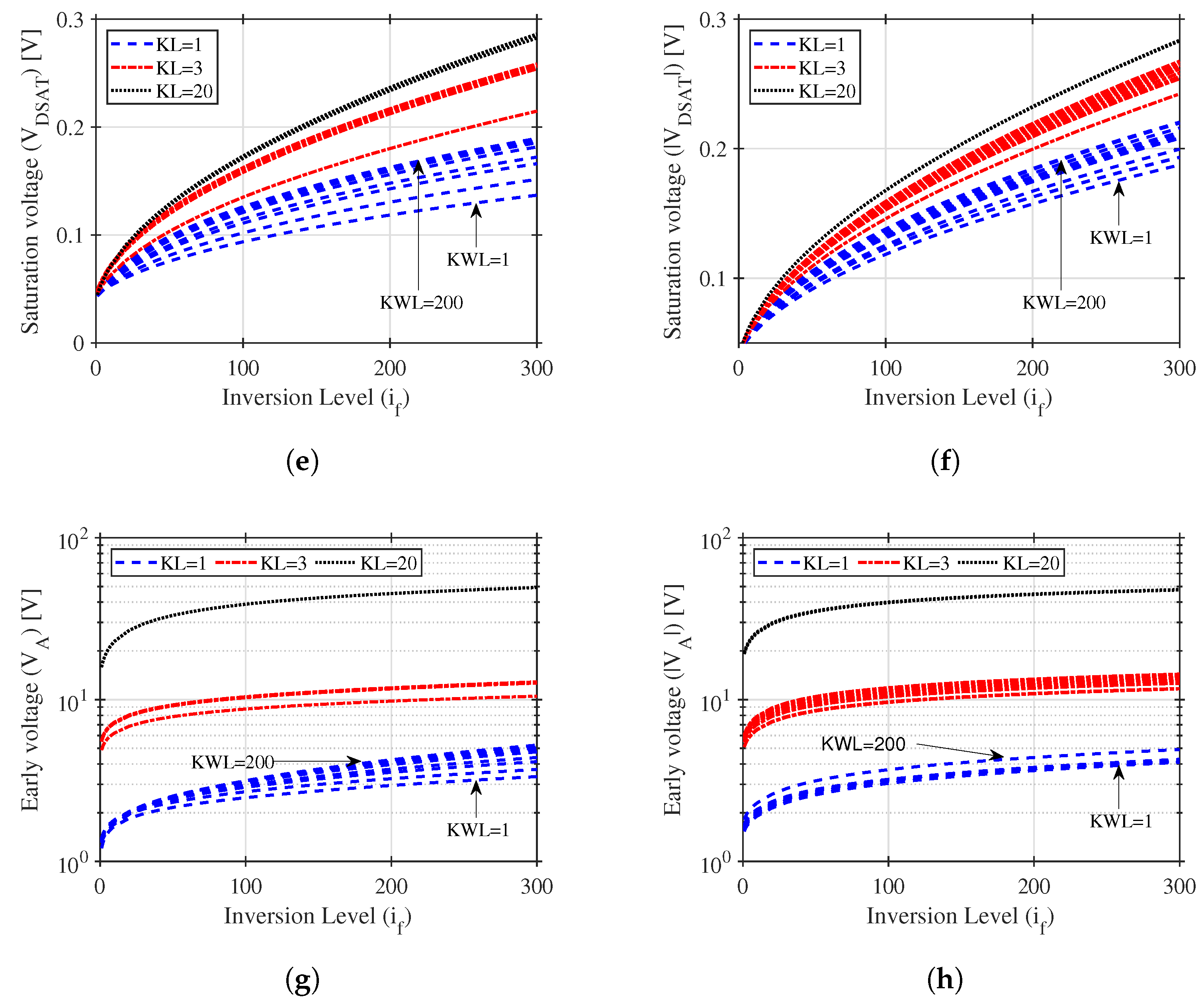
3.2. Advanced Compact MOSFET (ACM) Model

ACM is a model based on the device physics of the MOS transistors similar to other charge-based models like EKV and BSIM5 [20,29,30]. The ACM model provides higher accuracy compared to the square-law model traditionally used for circuit design. This model is built with a small set of equations valid for all the regions of operation of the MOSFET transistor, providing continuous modeling of the I/V characteristics of the device from deep saturation (strong inversion) to sub-threshold operation (moderate to weak inversion). A particular subset of the ACM equations are of interest for the formulation of our surrogate: the source trans-conductance g m (Equation (1)), the inversion level i f (Equation (2)), and the normalization current I S (Equation (3)).
g m = 2 I D ϕ t n 1 + 1 + i f
i f = I D I S
I S = W L μ n C o x ϕ t 2 2 ,
where I D is the drain current, ϕ t is the thermal voltage, ( W / L ) is the device aspect ratio, n is the slope factor, μ is the mobility, and C o x is the oxide capacitance per unit area. The inversion level of the transistor is of particular importance as it provides information about the operating point of the transistor without computing the potential at the gate of the device.
Although the base ACM model does not include short-channel effects or the dependency of the mobility on the transversal field, the model can be expanded to account for these effects [29,30]. However, many of the additional parameters needed to properly model these higher-order effects can be challenging to extract from simulation accurately. Instead, in our proposed model, we rely on non-parametric regression to account for higher-order effects and process variations.

3.3. Gaussian Process-Based Regression Models of the Process Characterization

The scaling trend on CMOS devices has resulted in not only smaller channel lengths and thinner gate-oxides, but also in the introduction of increasingly complex device structures and doping profiles [2,29]. To accurately predict the behavior of modern MOSFETs, device models have become more elaborated, introducing hundreds of device parameters, and making them impractical to use outside of the simulators available in specialized CAD software tools. To build our surrogate model, the behavior of the key parameters of the device must be accurately formulated as functions of design variables that are at the control of the designer. For our surrogate model, the parameters required are the oxide capacitance per unit of area ( C o x ), the normalization current ( I S ), the threshold voltage ( V T H ), the saturation voltage ( V D S A T ) and the early voltage ( V A ), the latter of which is used to estimate the output conductance of the transistor ( g d s = I D / V A ).
Once the parameters have been characterized against design variables, a prediction model must be created that can accurately approximate the data and can be used in conjunction with the remaining parts of our surrogate. Since the behavior of the parameters in question is complex and irregular, particularly with devices that exhibit significant short-channel and narrow-channel effects, using traditional equation-based curve-fitting techniques can become challenging and impractical. Therefore, it is attractive to consider non-parametric methods, that when properly configured, can approximate such complex irregular behaviors with significant ease and low error. In this work, Gaussian process regression is used to generate prediction models for the parameters in our surrogate.

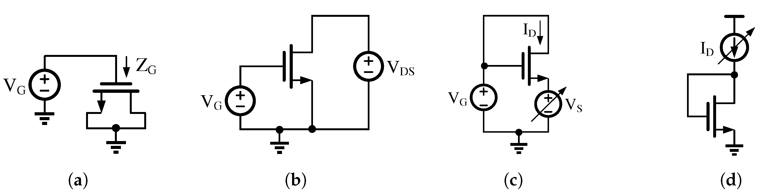
3.3.1. Characterization of the Parameters of CMOS Transistors

In theory, the normalization current I S (Equation (3)) depends only on the aspect ratio W / L of the transistor. However, in modern-day technologies, I S also varies with the dimensions of the device, as they can have a direct impact on the device’s mobility ( μ ). This makes the inversion level of a transistor a function of both W and L. Moreover, both the saturation voltage V D S A T and the early voltage V A exhibit a dependency on the inversion level of the transistor [30,31,32]. Finally, due to a combination of both short-channel and narrow-channel effects in modern CMOS processes, the threshold voltage ( V T H ) is also a function of both W and L [29].
The transistor is configured in a particular setup to characterize each parameter of CMOS transistors. Figure 2a shows the extraction setup for the oxide capacitance, where an AC signal is injected at a specific frequency while sweeping the DC bias at the gate, the capacitance is then computed from the impedance seen at the gate when the transistor is in the accumulation region. Figure 2b shows the schematic for the characterization of V T H , where W and L are varied. Also, the transistor is configured as shown in Figure 2c to extract the normalization current for each value of W and L. The voltage at the source terminal controls the forward inversion level while the diode-connection configuration avoids the effects of the reverse inversion [30]. The normalization current is then extracted from the g m / I D curve of the transistor based on Equation (1). Finally, the information of the normalization current is used to bias the transistor in specific forward inversion levels (Figure 2d) for which the early voltage and the saturation voltage are extracted. Figure 3 shows some samples of the data extracted from the characterization of the TSMC 180 nm process. The sizes of the transistor are normalized with respect to the minimum dimensions of the technology, such that L = K L L m i n and ( W / L ) = K W L ( W m i n / L m i n ) . Moreover, the characterization data is extracted for all process corners of interest and for each fabrication process to build the surrogate.

3.3.2. Gaussian-Processes-Based Regression Models

Large data-sets of the device’s parameters are acquired through the characterization process. The next step to complete our surrogate is to generate regression models capable of accurately estimating the required device’s parameters over all the possible design values. One alternative of doing this is through polynomial regression, as done previously in Reference [16]. However, the parametric nature of this approach limits the precision achievable in modeling the complex combination of short-channel and narrow-channel effects on modern CMOS devices. Non-parametric methods, on the other hand, can achieve higher precision by allowing the number of parameters to increase as dictated by the sample size.
Gaussian Process Regression (GPR) is a type of non-parametric method used in classification and regression models for Bayesian optimization or machine learning [9]. GPR models have gained popularity due to its probabilistic nature, which can model fairly complicated functional forms with high accuracy [9,23,33]. Instead of specifying a particular function for regression, a Gaussian Process defines a probability distribution over a function-space defined by the data-set. When a GPR model is evaluated, an inference takes place, providing a function y = f ( x ) within the function-space. The mean function m ( x ) and covariance function k ( x 1 , x 2 ) are what define a GPR model and determine the function-space generated from the data-set. While the mean function is commonly assumed constant and in many cases set to zero, the covariance function establishes the expected similarity or nearness between data points. By carefully choosing the covariance function one can embed the model with prior knowledge about the objective function to improve the predicting accuracy of the model [34]. A regression GP model is built from a training set D ( X , y ) where X = { x 1 , x 2 , , x N } denotes the input vectors with N observations, and y represents the corresponding outputs [34,35].
The mathematical software MATLAB® has in-built functions for training GPR models, make output predictions, calculate the regression loss, and even perform hyper-parameter optimization [36]. The function for the training of GP regression models fitrgp has a large number of parameters with several configuration options [36]. Therefore, in this work, a script selects the options of the fitrgp function that minimizes the prediction error. Such parameters are the kernel or the covariance function, the fitting method, the prediction method, and the active set selection method. For instance, Table 1 summarizes the best configuration for the training of GP models for the TSMC 180 nm technology. The GPR models of C o x , V T H , V A , I S , and V D S A T are created using the optimal parameters. The prediction function receives the GPR model and a set of design variables’ values and returns the corresponding value of the parameter. The main advantage of using a regression model is that it can predict the parameter values not only for the characterization data but also for points in between.

3.4. Circuit Performance Equation-Based Model

So far, the components of the surrogate model represent the fabrication process and the MOSFET device but are independent of the circuit topology. The third component corresponds to the equations-based model describing the performance metrics of an analog IC circuit. Such equations are derived using macromodel device representation and conventional circuit analysis techniques [2]. For the scope of this work, the equations were extracted manually. However, tools for automatic model generation using symbolic analysis [37], graph-based analysis [1] or signal path analysis could be used as an alternative if needed.
In Section 4, we compile three analog circuits with equations of their performance metrics that will be used to demonstrate the usefulness of the surrogate model. The circuit equations use the GPR models to compute the small-signal parameters needed for each particular transistor, provided the device dimensions and current bias are known. C o x , V T H and I S are evaluated directly from device dimensions. I S is used to compute the inversion level of the transistor (Equation (2)), which is necessary to calculate the device’s transconductance (Equation (1)) and evaluate the GPR models for V D S A T and V A .

3.5. Process Variations-Aware Automatic Design

Although smaller technologies allow high device integration, they tend to suffer from higher process variations in the fabrication process that are particularly harmful to the performance of analog integrated circuits. Several techniques for process-aware design rely on either worst-case analysis or Monte Carlo analysis. The worst-case analysis use corner models to estimate performance variations. Despite being a simple and fast approach, it might be pessimistic and can lead to over-design. On the other hand, Monte-Carlo analysis is a statistical method that can approximate variations with low error. However, it requires hundreds of samples, making it computationally expensive for large designs with time-consuming simulations.
Since the main goal of this surrogate model is to reduce the computational complexity of models, we use worst-case analysis to ensure robust solutions. The GPR models created from the characterization of the technology includes information of the nominal and corner models. This allows the surrogate to estimate the robustness of the solutions to process variations.

4. Experimental Results

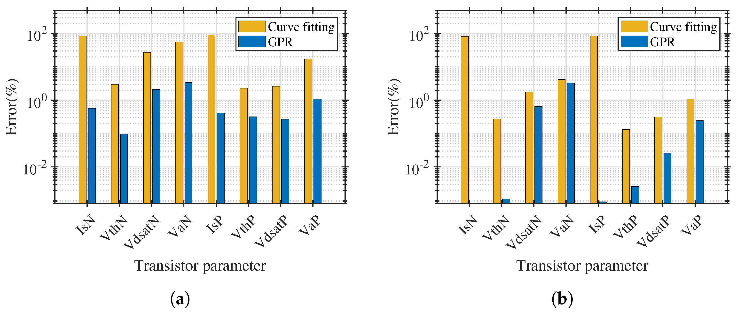
4.1. Error of the GPR-Based Surrogate Model

In this subsection, we evaluate the accuracy of the GPR model used in this work. As mentioned in Section 3 the process-dependent parameters of CMOS devices are characterized in terms of design variables and stored. Figure 4 shows the comparison of the percentage error of the parameter’s prediction using the curve-fitting-based models from Reference [16], and the GPR models developed in this work, with respect of circuit simulations (high-fidelity model). The accuracy of the models is evaluated for a small (Figure 4a) and large (Figure 4b) device size of the NMOS and PMOS devices on the TSMC 180 nm process. Note that the Y-axis has a logarithmic scale to visualize the error of the GPR that in all cases is lower than using a curve-fitting approach for prediction. Because the curve fitting model highly depends on the type of function and the number of coefficients used for the fitting, its accuracy is limited. As shown in Figure 4, the prediction error of the GPR models is smaller than 4% for all the parameters. Note that the prediction error of the NMOS’ normalization current ( I s N ) in Figure 4b is lower than 0.0001 % , and therefore, it is not visible on the plot.

4.2. Experimental Setup

The surrogate model is built for three technology nodes and three different circuit topologies. For each process, the model includes data of the nominal corner (TT) and the worst-case corners (SS, FF); all of them are considered simultaneously in the optimization. Then, the model is inserted on the iterative loop of state-of-the-art optimization algorithms, SQP and NSGA-II, to demonstrate the compatibility of our approach with different algorithms. The configuration of the main parameters of the algorithms used for the experiments is summarized in Table 2. The stop criterion is probably the most relevant parameter. The execution of the SQP algorithm ends when the solver takes a step that is smaller than the function tolerance, and the constraints are satisfied within the constraint tolerance [36]. If the execution does not achieve the minimum function tolerance, the algorithm stops when it reaches the maximum number of iterations or the maximum number of function evaluations. On the other hand, the NSGA-II algorithm stops when it reaches the maximum number of generations. Additionally, each optimization algorithm runs 10 times for the same optimization problem, keeping only the best results. Another difference in the operation of the algorithms is the construction of the Pareto front. While NSGA-II builds the Pareto using in-built functions for ranking and crowding distance calculation, that is not the case of the SQP algorithm. The gradient-based optimization with nonlinear constraints minimizes the weighted sum of all the objective functions. Therefore, each point of the Pareto front is obtained by modifying the weights of the objectives. Finally, NSGA-II requires distribution indexes for the operators of crossover and mutation [25].
The surrogate is self-contained and easily adaptable to other optimization techniques like differential evolution [10,14,23], simulated annealing [12], particle swarm optimization [4], Bayesian optimization [9], and even learning-based techniques like neural networks or support vector machines [8]. The optimization framework is implemented in MATLAB® using in-built functions combined with optimization toolboxes [25,36]. Finally, the solutions are evaluated by circuit simulation (high-fidelity model) using the Cadence® Spectre® Simulator, and any solutions not found in compliance with the specifications, on all the corners, are discarded. All experiments were executed in a Linux workstation with an Intel Xeon CPU with frequency 2.3 GHz and 131 GB of RAM memory.

4.3. Active-RC Second Order Filter

Filters are key building blocks in signal processing, allowing the suppression or selection of specific frequency bands. The requirements of the filter type, order, bandwidth, and selectivity may change depending on the application. In this test case, the proposed framework provides designs of the Tow-Thomas 2nd-order Butterworth active-RC low-pass filter (LPF) as shown in Figure 5a. This filter topology is widely used because of its ease of tunability and relatively low sensitivity to component variation. The transfer function of the filter in standard second-order form is shown on Equation (4), where Q represents the selectivity (5) and ω 0 indicates the center frequency (6). These expressions do not take into account the effect of the frequency response of the amplifiers, which can lead to Q-enhancement and center-frequency errors [38]. Instead, these effects are taken into consideration on the bandwidth requirements of the amplifiers.
H L P ( s ) = ω 0 2 s 2 + s ω 0 / Q + ω 0 2
Q = R Q / R
ω 0 = 1 / R C .
The two-stage internally-compensated topology shown in Figure 5b is used on the implementation of the amplifiers in the filter ( A 1 , A 2 , and A 3 ). This amplifier consists of two gain stages: 1st-stage a PMOS differential pair with NMOS active-load, and 2nd-stage an NMOS common-source amplifier. The miller-capacitor ( C C ) performs stability compensation via pole-splitting.
From the transfer function of the filter, it can be straightforward to obtain a set of capacitor and resistor values to meet certain specifications of ω o and Q. However, on an integrated solution, the selection of these values can have a significant impact on the power and area cost of the circuit. Depending on the technology, the density of the available passives will change, and the sizing of the resistors and capacitors to implement a specific time-constant will have direct consequences on the loading and stability requirements of the amplifiers as well as the noise performance of the filter. To successfully design a power and area efficient filter, one must optimize the resistor and capacitors in conjunction with the sizing of transistors in the amplifiers to guarantee a certain desired performance. Within this context, the optimization problem is defined as follows:
Minimize ( α a · Area ( x , p ) + α p · Power ( x , p ) )
x = [ K I B , K L , K W L B 1 , K W L I , K W L L , K W L S , K W L B 2 , K C C , K C ]
subject   to   x lb x x ub ,   and   g ( x , p ) 0
g ( x , p ) = [ A 0 , U G F , P M , O S , I C M R , S R , V N ]
where x is the set of normalized optimization variables, which includes: biasing conditions ( I B = K I B × 1 μ A ), transistor’s length ( L = K L × L m i n ), aspect ratios ( W / L i = K W L i ) and capacitor values ( C C = K C C × 100 f F , C = K C × 1 p F ), with L m i n as the minimum channel length of the technology. The set of constant parameters is p = [ Q , F C ] , which is meant to represent system-level requirements outside of the control of the design, where F C = 2 π ω 0 for Q = 0.707 (Butterworth filter). The resistor values of the filter are not considered design variables, as they are automatically derived by specifying the capacitor (C) value and the filter specifications. In addition, the non-equality constraints g considered are the amplifier’s DC gain ( A 0 ), unity-gain frequency ( U G F ), phase margin ( P M ), input common-mode range ( I C M R ), output swing ( O S ), slew rate ( S R ) and input-referred spot noise ( V I N ). Although linearity is not explicitly considered as a constraint in the surrogate, it can be adjusted as needed by changing the gain specification of the amplifiers, taking advantage of the linearization properties of negative feedback [39]. For other topologies that can not rely on negative feedback to improve linearity, a specific linearity specification could be included in the surrogate.

4.3.1. Surrogate of the Filter’s Performance Metrics

To complete the surrogate model for the circuit, a system of equations was formulated using known approximations of the performance metrics of the amplifier. The amplifier’s DC gain is A 0 = g m I g m S R 1 R 2 , where R 1 = 1 / ( g d s L + g d s I ) and R 2 = 1 / ( g d s S + g d s B 2 + 1 / R L ) are the output impedances associated with each stage of the amplifier, with R L as the load seen by the amplifier due to the resistors in the filter. The unity gain frequency is shown on Equation (7), where ω p 1 and ω p 2 are the poles at the output of each gain stage in the amplifier, given by Equations (8) and (9) respectively. The phase margin is given by P M 180 ° tan 1 U G F / ω p 1 tan 1 U G F / ω p 2 tan 1 U G F / ω z , with ω z = g m s / C C as the feed-forward zero created by the miller capacitor. The input common-mode range is computed as: I C M R = V D D | V D S A T B | | V D S A T I | V T H L V D S A T L , and the output swing as: O S = V D D | V D S A T B 2 | V D S A T S 2 , where V D D represents the nominal supply-voltage for the given technology. The slew-rate is approximated to be the minimum of either S R 1 = I B / C C or S R 2 = I B 2 / ( C C + C ) , where I B 2 = ( K W L B 2 / K W L B 1 ) × I B is the current bias of the amplifier’s second stage. Noise equations to compute input-referred spot noise from both white and flicker noise sources are also included [40].
U G F 1 8 π 4 A 0 2 ω p 1 2 ω p 2 2 2 ω p 1 2 ω p 2 2 + ω p 1 4 + ω p 2 4 ω p 1 2 ω p 2 2
ω p 1 = 1 R 1 C C + R 2 ( C C + C L ) + g m s R 1 R 2 C C
ω p 2 = R 1 C C + R 2 ( C C + C L ) + g m s R 1 R 2 C C R 1 R 2 C C C L
Finally, for the objective functions: power consumption is given by P W R = 3 × ( 2 I B + I B 2 ) ( V D D ) and the area cost (A) of the design is calculated as shown by Equation (10). Where C P A is the capacitance per unit of area, R S is the sheet resistance and W R is the resistor width, all of which are process-dependent parameters.
A = 3 × ( L ) 2 ( 2 K W L B 1 + K W L B 2 / K W L B 1 ) K W L B 1 + 2 K W L I + 2 K W L L + K W L S + 2 × ( C C + C ) / C P A + ( 5 + Q ) R / R S ( W R ) 2 .
The surrogate also includes equations to make sure that all transistors are properly biased outside the triode region ( V D S A T < V D S ) based on the common-mode signal level at the input ( V C M ) and above weak inversion ( i f > 1 ) [29,32].

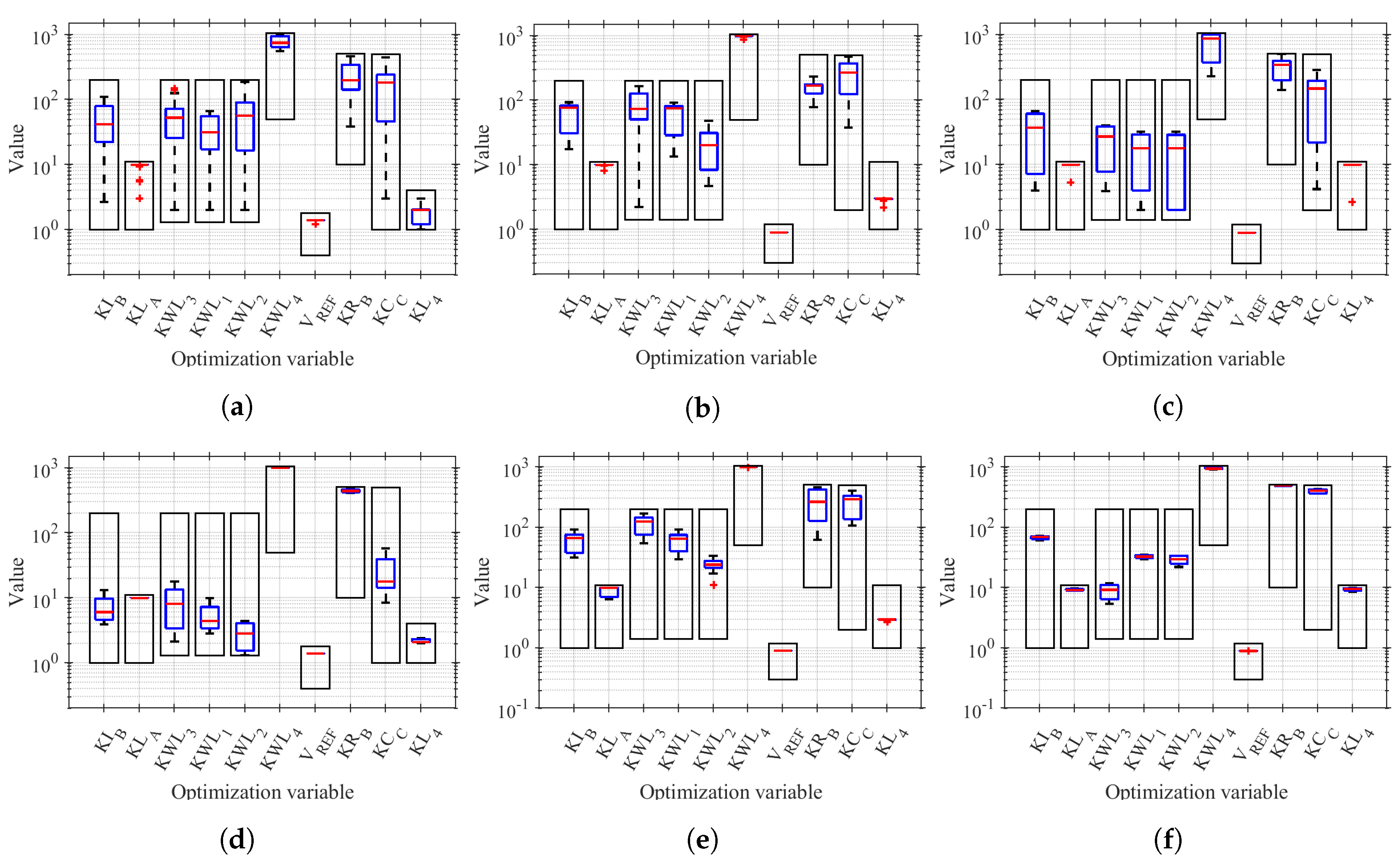
4.3.2. Results of Filter’s Automatic Design

As described in Section 3, once the optimizer generates a set of solutions, they are verified through circuit simulation in the high-fidelity model to obtain the final performance metrics. Figure 6 shows the design trade-off between minimization objectives (power, area) for the three technology processes (TSMC 180 nm, IBM 130 nm, TSMC 65 nm) and both optimization algorithms (SQP, NSGA-II) with a specification of F C = 100 KHz. From the Pareto we can take notice that the solutions generated in the 180 nm process can provide lower area costs than in the 130 nm, this is due to the fact that the sheet resistance ( R S ) of the selected resistor in the 130 nm process was smaller, resulting in a larger area consumption in comparison with the solutions in the 180 nm process. Similarly, the higher density of passives on the 65 nm process allows for much lower area metrics compared to the other technologies. However, the power consumption is also higher, likely due to the reduced intrinsic gain of the smaller process. Also, worth mentioning is that even though the NSGA-II optimizer generated a larger set of solutions, only a small subset of them were competitive enough to be included in the Pareto comparison with SQP.
Figure 7 shows a set of box plots comparing the design variables ( x ) in the Pareto’s solutions, allowing us to gain insight in which design variables are more tightly restricted for an optimal design, an overlay box with each variable allowed range is included for reference. For example, in all cases the biasing current ( I B ) is kept low, even going so far as to reach the lower boundary set for the variable in some cases, which relates to the direct impact its value has on the power consumption objective.
Table 3 shows a summary of constraints for one set of Pareto solutions (SQP optimization, 180 nm technology) evaluated through process variations for different desired filter cut-off frequencies ( F C ), where the U G F specification was set to be at least 10 times larger than the F C parameter to minimize the effect of Q-enhancement and center-frequency errors. The comparison on the table reveals how different constraints become active or inactive as the bandwidth requirements change, where an active constrain is one that is satisfied by a narrower margin, indicating it might be a bottleneck for the design. For example, as the frequency requirements increase, the A 0 specification is more narrowly satisfied while the S R constrain is relaxed, which is a direct consequence of the increased biasing required to reach a higher U G F specification. The U G F requirement is also more tightly met at higher F C specifications, which is to be expected since it directly conflicts with the minimization of power consumption in the optimizer. All solutions are viable and comply with the desired specifications across corners. In all cases, the cut-off frequency specification is satisfied within a worst-case 8 % error, which is consistent with the UGF requirement set for the optimizer. Thus, for the case of the 2nd-order Butterworth LPF, the proposed surrogate model design framework was demonstrated to generate viable solutions across process variation, technologies, frequency requirements, and optimization algorithms, all while providing insightful trade-offs in the constraints and objectives of the design.

4.4. Capacitor-Less Low-Dropout (CL-LDO) Voltage Regulator

In the second case example, we present the optimization of a capacitor-less low-dropout (CL-LDO) voltage regulator with a PMOS pass transistor and a single-stage error amplifier as shown in Figure 8 [41]. This circuit provides a clean and stable output voltage V O set by the reference voltage V R E F and the voltage divider implemented by R F 1 and R F 2 . The dropout voltage V D O = V I N V O is the minimum difference between input and output voltage to maintain regulation. The pass transistor M 4 is sized such that its output impedance r d s = 1 / g d s complies with the load current and the voltage across V D O . This topology uses a type-A error amplifier due to its inherent good power supply rejection (PSR) [41]. Most importantly, this LDO topology does not require an external large capacitor at the output for stability purposes. Instead, the circuit is internally compensated by an integrated compensation capacitor C C that adds to the already large parasitic capacitors of the pass transistor. The CL-LDO is a particularly good fit for optimization-aided design, as the circuit requirements must be satisfied across the load range, particularly balancing the trade-off between good PSR and sufficient stability.
For the purpose of this example, the LDO shown will be designed to meet a set of specifications of power supply rejection (PSR) at different frequencies, phase margin, input common-mode range and output swing of the error amplifier. With the objective of minimizing the quiescent power P q u i e s c e n t [ W ] and the power supply rejection at DC ( P S R @ D C [ V / V ] ). The total active area is not considered for optimization because it is dominated by the area of the pass transistor, which is defined by the range of the load current. The optimization problem is defined as follows:
minimize   P quiescent ( x , p ) ,   PSR @ DC ( x , p )
subject   to   x lb x x ub ,   and   g ( x , p ) 0
x = [ K I B , K L A , K W L 3 , K W L 1 , K W L 2 , K W L 4 , V R E F , K R B , K C C , K L 4 ] ,
where the set of normalized design variables x , includes the biasing conditions of the amplifier ( I B = K I B × 1 μ A ), transistors lengths ( L i = K L i × L m i n ) and aspect ratios ( W / L = K W L i ), reference voltage ( V R E F ), the output sampling resistor ( K R B ) and compensation capacitor ( C C = K C C × 1 pF ). Note that K R B × 1 k Ω = R F 1 + R F 2 .

4.4.1. Surrogate of the LDO’s Performance Metrics

Small signal analysis techniques are used to build the component of the surrogate related to the performance metrics of the circuit under design.
Figure 9 shows the small-signal macromodel for calculating the PSR of the LDO. The transfer function of the macromodel ( V O ( s ) / V I N ( s ) ) was obtained by using circuit analysis techniques like modified nodal analysis (MNA). Similarly, the macromodel for obtaining the expression of the loop gain and the phase margin is shown in Figure 10.
In order to simplify the analysis let us define the auxiliary variables: R 1 = 1 / ( r d s 1 | | r d s 2 ) , R 2 = r d s 4 | | V o / I L , C 1 = C g s 4 + C g b 4 + C E A , C 2 = C g d 4 + C C and C I N = C g s 1 . The symbolic expressions of three poles (11)–(13) and the zero f z = g m P / ( 2 π C 2 ) were extracted from the loop transfer function.
The phase margin is evaluated as P M = 180 ° tan 1 ( U G F / f p 1 ) tan 1 ( U F G / f p 2 ) tan 1 ( U G F / f p 3 ) tan 1 ( U G F / f z ) , where U G F is the unity gain frequency. While these expressions are impractical for hand calculations, they are compatible with the proposed surrogate model enabling high accuracy. Finally, biasing conditions are included in the constraints to ensure that the transistors do not operate in the linear region V D S A T < V D S . Also, the minimum inversion level is controlled such that the transistors will operate in moderate to strong inversion levels i f > 1 . Thus, the equation V D S A T 4 < ( V I N V O ) is included in the set of constraints. Biasing equations of the error amplifier are also included: ( V T H 1 + V D S A T 1 + V D S A T 3 ) < V R E F and ( V R E F < ( V I N + V T H 1 | V T H 2 | | V D S A T 2 | ) .
f p 1 R 2 + R f 1 + R f 2 ( 2 π ) C L R 2 R f 1 + C I N R 2 R f 2 + C L R 2 R f 2 + C I N R f 1 R f 2 + C 2 R 2 ( R f 1 + R f 2 ) + C 1 R 1 ( R 2 + R f 1 + R f 2 ) + C 2 R 1 ( R 2 + R f 1 + R f 2 + g m P R 2 ( R f 1 + R f 2 ) )
f p 2 C L R 2 R f 1 + C I N R 2 R f 2 + C L R 2 R f 2 + C I N R f 1 R f 2 + C 2 R 2 ( R f 1 + R f 2 ) + C 1 R 1 ( R 2 + R f 1 + R f 2 ) + C 2 R 1 ( R 2 + R f 1 + R f 2 + g m P R 2 ( R f 1 + R f 2 ) ) ( 2 π ) C I N C L R 2 R f 1 R f 2 + C 2 C I N ( R 2 R f 1 + R 1 ( R 2 + R f 1 + g m P R 2 R f 1 ) ) R f 2 + C 2 C L R 1 R 2 ( R f 1 + R f 2 ) + C 1 R 1 ( C I N ( R 2 + R f 1 ) R f 2 + C 2 R 2 ( R f 1 + R f 2 ) + C L R 2 ( R f 1 + R f 2 ) )
f p 3 C I N C L R 2 R f 1 R f 2 + C 2 C I N ( R 2 R f 1 + R 1 ( R 2 + R f 1 + g m P R 2 R f 1 ) ) R f 2 + C 2 C L R 1 R 2 ( R f 1 + R f 2 ) + C 1 R 1 ( C I N ( R 2 + R f 1 ) R f 2 + C 2 R 2 ( R f 1 + R f 2 ) + C L R 2 ( R f 1 + R f 2 ) ) ( 2 π ) C I N ( C 2 C L + C 1 ( C 2 + C L ) ) R 1 R 2 R f 1 R f 2 .

4.4.2. Results of the LDO’s Automatic Design

As with the previous test case, the CL-LDO circuit was designed using three different fabrication processes (TSMC 180 nm, IBM 130 nm, and TSMC 65 nm), and two optimization algorithms: SQP and NSGA-II, for a total of 6 experiments. The circuit parameters and the specification constraints are summarized on Table 4.
The resulting set of solutions build the Pareto fronts in Figure 11. The trade-off between power consumption and PSR is evident in the Pareto fronts. The PSR of this LDO topology is related to the gain of the error amplifier. Since higher gain requires higher power consumption, the two objectives can not be improved simultaneously. Comparing the Pareto fronts obtained using both optimization algorithms we do not observe a clear dominance of one algorithm on finding the best solutions for all designs. Regardless, the surrogate model fits well both optimization algorithms and enables them to find different sets of valid solutions. The large set of solutions found by the algorithms and verified with circuit simulations prove the high-accuracy of the surrogate model including process variations.
The variable with the smallest distribution is V R E F that consistently tends to the same value across all solutions. We also observe a clear tendency for the algorithms to maximize K L A (since its maximum value is 10) to increase the gain of the error amplifier and therefore increase the |PSR|. The aspect ratio of the pass transistor K W L 4 in most of the cases tends to the maximum allowed value. The other variables have a larger distribution of values over their ranges and their tendency is similar for both algorithms. Moreover, the range of the values obtained using NSGA-II is narrower than the one obtained with SQP.
Box plots of the values of each optimization variable were created to determine the diversity of the solutions in the Pareto front as shown in Figure 12. For comparison purposes, Figure 12 also shows the whole range of each design variable.
To verify the constraints, we extracted the min, mean and max values of the specifications estimated through circuit simulations. The results of the optimization case SQP/130 nm are reported in Table 5, while the ones of the case NSGA-II/130 nm are presented in Table 6. Within these constraints evaluated for the nominal corner only, the PSR@10kHZ and the PSR@100kHZ appears to be active constraints, while other constraints like phase margin seem more relaxed (non-active). The fact that the designs display over-design of the phase margin specification has several possible explanations. First, that despite it is not an active constraint in the nominal corner TT, it becomes one once it is evaluated for the case of the worst-corners. Second, that there is some discrepancy in the surrogate model, particularly on the estimation of the capacitances and resistances associated with the dominant and output nodes. Third, that given the range or search space of each variable, there is no such solution that could reduce the phase margin while still satisfying the PSR constraints.

4.5. Current-Starved Voltage Controlled Oscillator (CSVCO)

Oscillators are a fundamental block in transceivers and Phase-Locked-Loops (PLLs) [42]. One of the most conventional implementations of an oscillator is the ring oscillator, which consists of an odd number of inverter cells arranged in a feedback loop. Current limiting transistors are added to control the frequency of oscillation, to the top and bottom of the inverter cell, commonly known as current starving.
In this test case we optimize the performance of the five-stage CSVCO shown in Figure 13 [21]. As shown in the schematic, the control voltage is generated by a current source I B and a diode-connected transistor.
The optimization problem is defined as follows:
minimize { P ( x ) , L ( Δ f , x ) }
subject   to   x lb x x ub ,   e ( x , p ) = 0 ,   and   g ( x , p ) 0
x = [ K I B , K L I , K W L N , K W L N I , K W L P , K W L P I , K L C ] ,
where the set of normalized design variables x , includes the biasing conditions for the current limiting transistors ( I B = K I B × 1 μ A ), transistors lengths ( L i = K L i × L m i n ) and aspect ratios ( W / L = K W L i ) for the transistor in the inverter and the biasing circuit.

4.5.1. Surrogate of the CSVCO’s Performance Metrics

Equations (14) and (15) describe some of the most important performance metrics of the CSVCO such as oscillation frequency ( f o s c ), total power (P), and phase noise ( L ) [21,43,44].
f o s c = I D N · V D D · C t o t C t o t 5 2 ( C o x W N I L + C o x W P I L )
P = P s h o r t c i r c u i t + P a v e r a g e L ( Δ f ) = 8 k T V D D f o s c 2 3 η P V c h a r Δ f 2 ,
where, I D is the inverter’s current, V D D is the supply voltage, C t o t is the total capacitance at the output of each inverter stage. W N I / L and W P I / L represent the aspect ratios of the NMOS and PMOS transistors, respectively.
Therefore, the optimization will provide the circuit sizing such that it meets the constraint of oscillation frequency while minimizing power and phase noise. Note that Δ f is the offset frequency from the carrier where the phase noise is sampled, and it is set to Δ f = 1 MHz for this experiment. Similar to the previous test cases, several constraints are also included to ensure that the transistors operate within moderate to strong inversion. However, this model does not account for errors in the current copy done by the current mirrors.

4.5.2. Results of the CSVCO’s Automatic Design

Figure 14 shows the trade-off between phase noise and power consumption when sizing the CSVCO for a frequency of oscillation f o s c = 1 GHz for the TSMC 180 nm and IBM 130 nm processes, or f o s c = 10 GHz for the TSMC 65 nm process. From the Pareto fronts, we observe that the range of solutions found by the NSGA-II algorithm is narrower to the one found by the SQP.
That is also reflected in Figure 15, where we observe a larger distribution of the variables of the solutions found using the SQP algorithm than the NSGA-II. Still, in both cases, the surrogate is accurate enough to allow both algorithms to find valid solutions across coroners verified through simulation.
The constraints were also verified with circuit simulation to ensure that all solutions included in the Pareto provide a sustained oscillation at f o s c = 1 GHz (TSMC 180, IBM 130) or f o s c = 1 GHz (TSMC 65), and that under corners, the error of this frequency is no larger than 1%.

4.6. Summary

The main contribution of this work is a surrogate model that is computationally inexpensive, allowing fast evaluation of the objective functions and constraints for the optimization-aided automatic circuit design.
An example of the evolution of the objective function through the optimization processes of both algorithms is illustrated in Figure 16. As expected, the objective function, considered here as a linear combination of the minimization objectives, reduces with the iterations (generations) until reaching the stop criteria. The SQP algorithm stops when the calculated step is smaller than the function tolerance, while the NSGA-II stops after reaching the maximum number of generations.
The test cases presented in this work are summarized in Table 7. The time required for the evaluation of objectives and constraints is compared when using the proposed surrogate and when using circuit simulations (using Ocean Cadence). Using the circuit simulator embedded in the optimization algorithm requires to write the parameters in the ocean file, source the software, run the simulation, and read the results. For example, in the case of the LDO, these operations take 0.6 s, 24.82 s, 1.18 s, and 5.5 ms, respectively. On the other hand, using the GP models require to load the models (41.58 s) and evaluate the model (17.84 ms). However, launching the simulation software and loading the GPR models happens only once in every execution of the optimization algorithm although these times seem large, they are negligible compared with the whole optimization run. Instead, the real target is to minimize the time required to evaluate a single solution since that will be repeated thousands of times in an execution. The number of evaluations in a single run depends on the number of iterations or generations, the size of the population, the stop criteria of the algorithm, and the number of multi-runs. Table 7 shows the comparison of the evaluation of a single candidate solution for all corners when using our surrogate vs the circuit simulator.
Note that the simulation time is heavily dependent on the type of analysis require to quantify certain metrics. For instance, measuring the slew rate requires a lengthy transient simulation in comparison to the phase margin that can be estimated with a faster AC simulation.
All results presented in the three test cases have been validated through simulation to verify all constraints are satisfied across process corners. Although the surrogate model uses highly accurate equations, avoiding simplification as much as possible, a margin of error in prediction is expected with respect to the high-fidelity model. One method to quantify the effectiveness of the surrogate for optimization-aided design is the success rate, which refers to the percentage of solutions generated through optimization using the surrogate that successfully comply with all specifications after being validated by circuit simulation. Table 8 summarizes the success rate of all the test cases across the three technology processes considered. Evaluating the solutions that fail to satisfy circuit simulations can help identify opportunities to enhance the surrogate’s precision. For example, in the case of the filter design in the TSMC 65 nm process, the specification of the Op-Amp’s DC gain is the most significant active-constraint. Due to the lower intrinsic gain of the smaller process, the constraint is usually narrowly met. Then, even small errors in precision on the surrogate can cause the solution to fall under the constraint limit. Most of the solutions deemed invalid in the SQP-optimized case fall under a 1 dB error in the DC gain specification, and if accounted for, result in an overall success rate improvement from 57.14 % to 83.33 % . In the LDO optimization, some of the solutions fail to meet all specifications for both low-load and high-load conditions. This error is mainly caused by the error in the estimation of the pass transistor parameter’s, the largest device; this error reduces by increasing the resolution in the characterization of the early voltage. The error in the VCO optimization is mostly caused by the mismatch on the current copy of the current mirrors, even a small error in the current copy causes a deviation in the oscillation frequency larger than 1 % when verified across corners.
Introducing additional details to the circuit model, such as current-mirror mismatch modeling could help improve the surrogate model in this regard. However, the additional effort required to increase the complexity of the model may not be justified if the valid solutions generated by the surrogate prove to be sufficient for the target application.

5. Conclusions

In this paper, we presented a low-computational cost and accurate surrogate model for automatic IC sizing. This surrogate has three main elements that make it modular and reusable for the design of analog circuits across topologies and CMOS processes. In particular, Gaussian process regression is used to generate high accuracy prediction models of key device parameters based on characterization data of devices through process variations, expanding the capabilities of the transistor model to account for short-channel and narrow-channel effects. The process-aware nature of our surrogate reduces the iterative circuit verification to reach a viable circuit solution, despite the required initial effort to create it. Moreover, the created model can be easily re-used, such that a circuit can be re-designed for new applications by only updating the objectives and constraints. The low-cost surrogate allows for faster evaluation, which can enable the optimization of larger problems, demonstrating an improvement in evaluation time from 69 X to 470 X compared to the high-fidelity model.
The topology-dependent component of the surrogate requires the analog designer to obtain the expressions of the performance metrics. Therefore, to add a new topology, some initial effort is required. However, once the model is created, the designer can store it in a database, and reuse it for optimization across technologies and various performance metrics. Having a database of the models of different topologies could also allow a comparison of their performances to aid the designer in the topology selection.
The proposed surrogate is integrated into a multi-objective constrained optimization framework with interchangeable state-of-the-art optimization algorithms. Then, the usage of our surrogate for automatic analog circuit design was tested on three different circuit topologies using three fabrication processes. The ability of our proposed surrogate to evaluate the circuit performance from the design variables was demonstrated by the generation of viable solutions across process corners independent of the optimization algorithm. Additionally, the use of our surrogate in conjunction with multi-objective optimization allows the designer to improve the exploration of the space of solutions and to gain insight into design trade-offs through the Pareto front.
Future work should focus on the characterization and modeling of the post-layout parasitic components and include them in the surrogate to enable efficient parasitic-aware automatic analog design.

Author Contributions

A.C.S.-B. and S.S.-A. have equal contributions on the development of the surrogate and its experimental validation. D.A. provided conceptual contribution in the area of Gaussian processes and optimization. J.J.E.-L. and E.S.-S. provided contribute writing—review and editing, funding acquisition and supervision of the project. All authors have read and agreed to the published version of the manuscript.

Funding

The authors would like to thank Texas Instruments, Qualcomm, and Silicon Labs for partial support.

Conflicts of Interest

The authors declare no conflict of interest.

References

  1. Scheffer, L.; Lavagno, L.; Martin, G. EDA for IC implementation, circuit design, and process technology. In Electronic Design Automation for Integrated Circuits Handbook; Scheffer, L., Lavagno, L., Martin, G., Eds.; CRC Taylor & Francis: Boca Raton, FL, USA, 2006. [Google Scholar]
  2. Razavi, B. Design of Analog CMOS Integrated Circuits; McGraw-Hill Education: New York, NY, USA, 2017. [Google Scholar]
  3. Gielen, G.G.E.; Rutenbar, R.A. Computer-aided design of analog and mixed-signal integrated circuits. Proc. IEEE 2000, 88, 1825–1854. [Google Scholar] [CrossRef]
  4. Fakhfakh, M.; Cooren, Y.; Sallem, A.; Loulou, M.; Siarry, P. Analog circuit design optimization through the particle swarm optimization technique. Analog Integr. Circuits Signal Process. 2010, 63, 71–82. [Google Scholar] [CrossRef]
  5. Fakhfakh, M.; Tlelo-Cuautle, E.; Siarry, P. Computational Intelligence in Analog and Mixed-Signal (AMS) and Radio-Frequency (RF) Circuit Design; Springer: Cham, Switzerland, 2015; pp. 1–491. [Google Scholar]
  6. Rutenbar, R.A.; Gielen, G.G.E.; Roychowdhury, J. Hierarchical Modeling, Optimization, and Synthesis for System-Level Analog and RF Designs. Proc. IEEE 2007, 95, 640–669. [Google Scholar] [CrossRef]
  7. Goswami, M.; Kundu, S. Constrained Low-power CMOS Analog Circuit Design via All-Inversion Region MOS Model. In Proceedings of the 2014 IEEE Fourth International Conference on Consumer Electronics Berlin (ICCE-Berlin), Berlin, Germany, 7–10 September 2014; pp. 277–278. [Google Scholar]
  8. Rocha, F.; Martins, R.; Lourenço, N.; Horta, N. Electronic Design Automation of Analog ICs Combining Gradient Models with Multi-Objective Evolutionary Algorithms; Springer Briefs in Applied Sciences and Technology; Springer International Publishing: Cham, Switzerland, 2014. [Google Scholar]
  9. Lyu, W.; Xue, P.; Yang, F.; Yan, C.; Hong, Z.; Zeng, X.; Zhou, D. An efficient Bayesian optimization approach for automated optimization of analog circuits. IEEE Trans. Circuits Syst. I Regul. Pap. 2018, 65, 1954–1967. [Google Scholar] [CrossRef]
  10. Kubar, M.; Jakovenko, J. A Powerful Optimization Tool for Analog Integrated Circuits Design. Radioengineering 2013, 22, 921–931. [Google Scholar]
  11. Binkley, D.M.; Hopper, C.E.; Tucker, S.D.; Moss, B.C.; Rochelle, J.M.; Foty, D.P. A CAD methodology for optimizing transistor current and sizing in analog CMOS design. IEEE Trans. Comput. Aided Des. Integr. Circuits Syst. 2003, 22, 225–237. [Google Scholar] [CrossRef]
  12. Ochotta, E.S.; Rutenbar, R.A.; Carley, L.R. Synthesis of high-performance analog circuits in ASTRX/OBLX. IEEE Trans. Comput. Aided Des. Integr. Circuits Syst. 1996, 15, 273–294. [Google Scholar] [CrossRef] [Green Version]
  13. De Smedt, B.; Gielen, G.G.E. WATSON: Design space boundary exploration and model generation for analog and RFIC design. IEEE Trans. Comput. Aided Des. Integr. Circuits Syst. 2003, 22, 213–224. [Google Scholar] [CrossRef]
  14. Sanabria Borbon, A.; Tlelo-Cuautle, E.; de la Fraga, L. Optimal Sizing of Amplifiers by Evolutionary Algorithms with Integer Encoding and gm/ID Design Method. In NEO 2016. Studies in Computational Intelligence; Maldonado, Y., Trujillo, L., Schütze, O., Riccardi, A., Vasile, M., Eds.; Springer: Cham, Switzerland, 2018; Volume 731, pp. 263–279. [Google Scholar]
  15. Jespers, P.; Murmann, B. Systematic Design of Analog CMOS Circuits; Cambridge University Press: Cambridge, UK, 2017. [Google Scholar]
  16. Soto-Aguilar, S.; Sanabria-Borbón, A.; Sánchez-Sinencio, E. Surrogate-based Optimization-aided Design for Low Power Analog Circuits. In Proceedings of the 2018 IEEE 61st International Midwest Symposium on Circuits and Systems (MWSCAS), Windsor, ON, Canada, 5–8 August 2018; pp. 566–569. [Google Scholar]
  17. Graeb, H.; Schlichtmann, U. Pareto optimization of analog circuits considering variability. Int. J. Circuit Theory Appl. 2009, 22, 283–299. [Google Scholar] [CrossRef]
  18. Mueller-Gritschneder, D.; Graeb, H. Computation of yield-optimized pareto fronts for analog integrated circuit specifications. In Proceedings of the Design, Automation and Test in Europe, DATE, EDAA, Dresden, Germany, 8–12 March 2010; pp. 1088–1093. [Google Scholar]
  19. Damera-Venkata, N.; Evans, B.L. An automated framework for multicriteria optimization of analog filter designs. IEEE Trans. Circuits Syst. II Analog Digit. Signal Process. 1999, 46, 981–990. [Google Scholar] [CrossRef] [Green Version]
  20. Hershenson, M.D.M.; Boyd, S.P.; Lee, T.H. Optimal design of a CMOS op-amp via geometric programming. IEEE Trans. Comput. Aided Des. Integr. Circuits Syst. 2001, 20, 1–21. [Google Scholar] [CrossRef] [Green Version]
  21. Rout, P.K.; Acharya, D.P.; Panda, G. A Multiobjective Optimization Based Fast and Robust Design Methodology for Low Power and Low Phase Noise Current Starved VCO. IEEE Trans. Semicond. Manuf. 2014, 27, 43–50. [Google Scholar] [CrossRef]
  22. Mandal, P.; Visvanathan, V. CMOS op-amp sizing using a geometric programming formulation. IEEE Trans. Comput. Aided Des. Integr. Circuits Syst. 2001, 20, 22–38. [Google Scholar] [CrossRef]
  23. Liu, B.; Gielen, G.; Fernández, F.V. Automated Design of Analog and High-frequency Circuits. In Studies in Computational Intelligence; Springer: Berlin/Heidelberg, Germany, 2014; Volume 501. [Google Scholar]
  24. Nocedal, J.; Wright, S.J. Numerical Optimization, 2nd ed.; Nocedal, J., Wright, S.J., Eds.; Springer Series in Operations Research and Financial Engineering; Springer: New York, NY, USA, 2006. [Google Scholar]
  25. Deb, K.; Pratap, A.; Agarwal, S.; Meyarivan, T. A fast and elitist multiobjective genetic algorithm: NSGA-II. IEEE Trans. Evol. Comput. 2002, 6, 182–197. [Google Scholar] [CrossRef] [Green Version]
  26. Tlelo-Cuautle, E.; Sanabria-Borbon, A.C. Optimising operational amplifiers by evolutionary algorithms and gm/Id method. Int. J. Electron. 2016, 103, 1665–1684. [Google Scholar] [CrossRef]
  27. Lourenço, N. GENOM-POF: Multi-Objective Evolutionary Synthesis of Analog ICs with Corners Validation. In Proceedings of the 14th International Conference on Genetic and Evolutionary Computation (GECCO), Philadelphia, PA, USA, 7–11 July 2012; pp. 1119–1126. [Google Scholar]
  28. Mohanty, S.P. Nanoelectronic Mixed-Signal System Design; McGraw-Hill Education: New York, NY, USA, 2015. [Google Scholar]
  29. Schneider, M.C.; Galup-Montoro, C. CMOS Analog Design Using All-Region MOSFET Modeling; Cambridge University Press: Cambridge, UK, 2010. [Google Scholar]
  30. Cunha, A.I.A.; Schneider, M.C.; Galup-Montoro, C. An MOS transistor model for analog circuit design. IEEE J. Solid-State Circuits 1998, 33, 1510–1519. [Google Scholar] [CrossRef] [Green Version]
  31. Radin, R.L.; Moreira, G.L.; Galup-Montoro, C.; Schneider, M.C. A simple modeling of the early voltage of MOSFETs in weak and moderate inversion. In Proceedings of the 2008 IEEE International Symposium on Circuits and Systems, Seattle, WA, USA, 18–21 May 2008; pp. 1720–1723. [Google Scholar]
  32. Binkley, D.M. Tradeoffs and Optimization in Analog CMOS Design; John Wiley and Sons Ltd.: Chichester, UK, 2008. [Google Scholar]
  33. Liu, B.; He, Y.; Reynaert, P.; Gielen, G. Global optimization of integrated transformers for high frequency microwave circuits using a Gaussian process based surrogate model. In Proceedings of the 2011 Design, Automation Test in Europe, Grenoble, France, 14–18 March 2011; pp. 1–6. [Google Scholar]
  34. Rasmussen, C.E.; Williams, C.K.I. Gaussian Processes for Machine Learning; MIT Press: Cambridge, MA, USA, 2006. [Google Scholar]
  35. Zhang, S.; Lyu, W.; Yang, F.; Yan, C.; Zhou, D.; Zeng, X.; Hu, X. An Efficient Multi-Fidelity Bayesian Optimization Approach for Analog Circuit Synthesis. In Proceedings of the 56th Annual Design Automation Conference 2019 (DAC’19), Las Vegas, NV, USA, 2–6 June 2019; Association for Computing Machinery: New York, NY, USA, 2019. [Google Scholar]
  36. Matworks. Matlab Documentation R2019b. Available online: https://www.mathworks.com/help/releases/R2019b/index.html (accessed on 10 January 2020).
  37. Gielen, G.G.; Sansen, W.M. Symbolic Analysis for Automated Design of Analog Integrated Circuits; Kluwer Academic Publishers: Norwell, MA, USA, 1991. [Google Scholar]
  38. Franco, S. Design with Operational Amplifiers and Analog Integrated Circuits, 4th ed.; McGraw-Hill, Inc.: New York, NY, USA, 2015. [Google Scholar]
  39. Vereecken, W.; Steyaert, M. Ultra-Wideband Pulse-based Radio, 1st ed.; Springer: New York, NY, USA, 2009. [Google Scholar]
  40. Bruton, L.T.; Trofimenkoff, F.N.; Treleaven, D.H. Noise performance of low-sensitivity active filters. IEEE J. Solid-State Circuits 1973, 8, 85–91. [Google Scholar] [CrossRef]
  41. Torres, J.; El-Nozahi, M.; Amer, A.; Gopalraju, S.; Abdullah, R.; Entesari, K.; Sanchez-Sinencio, E. Low Drop-Out Voltage Regulators: Capacitor-less Architecture Comparison. IEEE Circuits Syst. Mag. 2014, 14, 6–26. [Google Scholar] [CrossRef]
  42. Razavi, B. RF Microelectronics; Prentice Hall Communications Engineering and Emerging Technologies Series; Prentice Hall: New York, NY, USA, 2012. [Google Scholar]
  43. Hajimiri, A.; Limotyrakis, S.; Lee, T.H. Jitter and phase noise in ring oscillators. IEEE J. Solid-State Circuits 1999, 34, 790–804. [Google Scholar] [CrossRef] [Green Version]
  44. Ghai, D.; Mohanty, S.P.; Kougianos, E. Design of Parasitic and Process-Variation Aware Nano-CMOS RF Circuits: A VCO Case Study. IEEE Trans. Very Large Scale Integr. Syst. 2009, 17, 1339–1342. [Google Scholar] [CrossRef]
Figure 1. Proposed surrogate model inserted on a modular optimization framework for automatic IC design.
Electronics 09 00685 g001
Figure 2. Schematics for device characterization of (a) Oxide Capacitance ( C o x ). (b) Threshold Voltage (VTH). (c) Normalization current (IS). (d) Saturation voltage (VDSAT). early voltage (VA).
Electronics 09 00685 g002
Figure 3. Sample of characterization data of a given CMOS technology in typical corner (TT) (a) NMOS: V T H . (b) PMOS: V T H . (c) NMOS: I S . (d) PMOS: I S . (e) NMOS: V D S A T . (f) PMOS: | V D S A T | . (g) NMOS: V A . (h) PMOS: | V A | .
Electronics 09 00685 g003aElectronics 09 00685 g003b
Figure 4. Comparison of the percentage error of prediction of CMOS parameters using models based on curve-fitting and Gaussian process regression (GPR) for sizes (a) KL = 1, KWL = 4. (b) KL = 10, KWL = 50. These models were built from the characterization data.
Electronics 09 00685 g004
Figure 5. Active-RC second order filter under design (a) circuit topology. (b) Transistor level schematic of the second order internally compensated amplifier.
Electronics 09 00685 g005
Figure 6. Pareto front of the optimization of filter (FC = 100 KHz) using SQP and NSGA-II optimization algorithms in (a) TSMC 180 nm CMOS process. (b) IBM 130 nm CMOS process. (c) TSMC 65 nm CMOS process.
Electronics 09 00685 g006
Figure 7. Values of the optimization variables from solutions in the Pareto front for the filter optimization (FC = 100 KHz) obtained with: (a) SQP-180 nm, (b) SQP-130 nm, (c) SQP-65 nm, (d) NSGA-II-180 nm, (e) NSGA-II-130 nm, and (f) NSGA-II-65 nm.
Electronics 09 00685 g007
Figure 8. Circuit schematic of the capacitor-less low dropout (LDO) with type-A single stage error amplifier internal frequency compensation provided by C C .
Electronics 09 00685 g008
Figure 9. Small-signal macromodel of the LDO for the calculation of the power supply rejection (PSR).
Electronics 09 00685 g009
Figure 10. Small-signal macromodel of the LDO for the calculation of the phase margin.
Electronics 09 00685 g010
Figure 11. Pareto front of the optimization of the LDO circuit using SQP and NSGA-II optimization algorithms and (a) TSMC 180 nm. (b) IBM 130 nm. (c) TSMC 65 nm CMOS process.
Electronics 09 00685 g011
Figure 12. Values of the optimization variables of the solutions in the Pareto front obtained with: (a) SQP-180 nm, (b) SQP-130 nm, (c) SQP-65 nm, (d) NSGA-II-180 nm, (e) NSGA-II-130 nm and (f) NSGA-II-65 nm
Electronics 09 00685 g012
Figure 13. Circuit schematic of a 5-stage current starved voltage controlled oscillator (VCO). The control voltage is generated with a biasing current and a diode connected transistor.
Electronics 09 00685 g013
Figure 14. Pareto front of the optimization of the CSVCO circuit using SQP and NSGA-II optimization algorithms and (a) TSMC 180 nm process. (b) IBM 130 nm process. (c) TSMC 65 nm CMOS process.
Electronics 09 00685 g014
Figure 15. Values of the optimization variables of the solutions in the Pareto front obtained with: (a) SQP-180 nm, (b) SQP-130 nm, (c) SQP-65 nm, (d) NSGA-II-180 nm, (e) NSGA-II-130 nm and (f) NSGA-II-65 nm.
Electronics 09 00685 g015aElectronics 09 00685 g015b
Figure 16. History of the objective function through the iterative optimization process using (a) SQP algorithm. (b) NSGA-II algorithm.
Electronics 09 00685 g016
Table 1. Optimal options of the function fitrpg for the training of the Gaussian Process (GP) model from the characterization of the process parameters in typical corner.
I S
NMOS
I S
PMOS
V TH
NMOS
V TH
PMOS
V DSAT
NMOS
V DSAT
PMOS
V A
NMOS
V A
PMOS
KernelFuncExp.ArdExp.ArdExp.ArdExp.Exp.Exp.Exp.ArdExp.
BasisFuncLinearNoneConstantNoneConstantConstantNoneNone
FitMethodFicFicSrSrSdSdFicSr
ActiveSetMethodSgmaSgmaRandomRandomEntropyRandomSgmaRandom
PredictMethodExactExactExactExactExactExactExactExact
ResubLoss1.37 × 10 5 3.5 × 10 7 6.26 × 10 8 11.52 × 10 8 5.18 × 10 7 2.35 × 10 7 6.29 × 10 6 2.47 × 10 5
Table 2. Parameters of the optimization algorithms used for this experiment sequential quadratic programming (SQP) and NSGA-II.
Parameter of the AlgorithmSQPNSGA-II
Algorithm implementationfmincon: sqp [36]NSGA2 toolbox [25]
Multi-start/Runs1010
Stop criteriaFunction tolerance = 1 × 10 17 Max. generations = 500
Max. Fun. evaluations = 8 × 10 5 Population size = 30
Other parametersMax. iterations = 2 × 10 6 Dist. index for crossover = 20
Constraint tolerance = 1 × 10 6 Dist. index for mutation = 20
Table 3. Performance metrics of the Pareto front solutions obtained through SQP optimization of the 2nd-order active-RC low-pass filter optimization in a TSMC 180 nm process (Noise ( V N ) reported at 10 kHz).
ParameterSpec FC = 100 KHz FC = 1 MHz FC = 10 MHz
MinMeanMaxMinMeanMaxMinMeanMax
A 0 [dB]>4055.5457.5961.3552.2155.6958.5842.4745.6549.24
U G F / F C >1019.2820.9831.8713.5915.0316.2611.7112.2713.34
P M [°]>4042.1745.4948.1642.3145.7549.2144.6246.9148.68
I C M R [V]>0.61.141.181.231.111.201.300.760.850.95
O S [V]>11.291.361.651.251.321.371.391.431.47
S R [V/ μ s]>0.42.132.383.6310.4012.2415.0685.8491.49103.63
0.560.661.154.735.536.4156.0257.1560.07
V N [ μ V/ Hz ]<20.891.041.221.221.341.411.051.111.18
Table 4. Circuit parameters and specification constraints for the optimization of the LDO in two different CMOS processes.
Process V IN V O C L I L , min I L , max PSR@1 kHzPSR@10 kHzPSR@100 kHzPM
TSMC 180 nm1.8 V1.6 V100 pF533.3 μ A5.3 mA<−50 dB<−45 dB<−25 dB>45°
IBM 130 nm1.2 V1 V100 pF333.3 μ A3.3 mA<−40 dB<−40 dB<−25 dB>45°
TSMC 65 nm1.2 V1 V100 pF333.3 μ A3.3 mA<−40 dB<−40 dB<−25 dB>45°
Table 5. Performance metrics of the Pareto front solutions obtained through SQP optimization of the CL-LDO in a 130 nm process measured with simulations.
MetricSpec.Low LoadHigh Load
MinMeanMaxMinMeanMax
|PSR@1kHz| [dB]>4040.2648.8154.4048.6254.0863.18
|PSR@10kHz| [dB]>4040.0445.5850.7144.7748.6754.41
|PSR@100kHz |[dB]>2527.8730.9934.5127.0230.7435.29
Phase Margin [°]>4549.3359.9168.6273.4081.0785.64
Table 6. Performance metrics of the Pareto front solutions obtained through NSGA-II optimization of the CL-LDO in the IBM 130 nm process measured with simulations.
MetricSpec.Low LoadHigh Load
MinMeanMaxMinMeanMax
|PSR@1kHz| [dB]>4040.3748.9759.7245.7856.6774.05
|PSR@10kHz| [dB]>4040.1947.1254.4545.3150.6056.27
|PSR@100kHz |[dB]>2531.5433.7536.4931.7133.9337.06
Phase margin [°]>4550.3953.3255.9970.8573.7877.42
Table 7. Summary of the test cases under optimization using the proposed surrogate model.
CircuitNo. of Design VariablesNo. of ConstraintsEvaluation Time Surrogate [s]Evaluation Time Simulation [s]Evaluation Time Improvement
Filter921 0.123 57.708 470 X
LDO1024 0.051 3.54 69 X
VCO715 0.063 18 285 X
Table 8. Summary of success rate from surrogate evaluation to simulation verification across corners.
CircuitTSMC180IBM130TSMC65
SQPNSGA-IISQPNSGA-IISQPNSGA-II
Filter90.48%68.57%100.00%100.00%57.14%100.00%
LDO76.67%70.00%70.00%83.33%56.67%75.45%
VCO60.00%66.67%70.00%93.33%86.67%60.00%

