Article

Simple Setup for Measuring the Response to Differential Mode Noise of Common Mode Chokes

by
Pablo González-Vizuete
1,
Carlos Domínguez-Palacios
1,
Joaquín Bernal-Méndez
2,* and
María A. Martín-Prats
1
1
Dpto.Ingeniería Electrónica, Escuela Técnica Superior de Ingeniería, Universidad de Sevilla, 41092 Seville, Spain
2
Dpto.Física Aplicada III, Escuela Técnica Superior de Ingeniería, Universidad de Sevilla, 41092 Seville, Spain
*
Author to whom correspondence should be addressed.
Electronics 2020, 9(3), 381; https://doi.org/10.3390/electronics9030381
Submission received: 15 January 2020 / Revised: 19 February 2020 / Accepted: 21 February 2020 / Published: 25 February 2020
(This article belongs to the Special Issue Electromagnetic Interference and Compatibility)

Abstract

:
This work presents a technique to measure the attenuation of differential mode noise provided by common mode chokes. The proposed setup is a simpler alternative to the balanced setup commonly employed to that end, and its main advantage is that it avoids the use of auxiliary circuits (baluns). We make use of a modal analysis of a high-frequency circuit model of the common mode choke to identify the natural modes actually excited both in the standard balanced setup and in the simpler alternative setup proposed here. This analysis demonstrates that both setups are equivalent at low frequencies and makes it possible to identify the key differences between them at high frequencies. To analyze the scope and interest of the proposed measurement technique we have measured several commercial common mode chokes and we have thoroughly studied the sensitivity of the measurements taken with the proposed setup to electric and magnetic couplings. We have found that the proposed setup can be useful for quick assessment of the attenuation provided by a common mode choke for differential mode noise in a frequency range that encompasses the frequencies where most electromagnetic compatibility regulations impose limits to the conducted emissions of electronic equipment.

1. Introduction

The control of conducted emissions of electronic devices is an increasingly critical topic due to the trends toward the use of higher switching frequencies in power converters [1]. To mitigate conducted emissions, power line electromagnetic interference (EMI) filters are commonly used. However, at frequencies ranging from several hundred kilohertz to a few tens of megahertz the performance of EMI filters is typically undermined by parasitic effects such as parasitic parallel capacitances between windings in inductors and parasitic series inductances of capacitors [2,3,4,5]. Therefore, characterizing the response of these components at those high frequencies is becoming increasingly important to reduce design time, cost and size of the filter.
Common mode chokes (CMCs), made up of a pair of tightly coupled inductors, are key components of EMI filters primarily intended to limit common mode (CM) noise [2,5]. However, CMCs typically exhibit an inductive response to differential mode (DM) noise (leakage inductance) which has a significant impact on the attenuation that the EMI filter provides to differential mode (DM) noise [2]. The reason is that the leakage inductance provides a 40 dB/dec roll-off above its frequency of resonance with capacitors that typically are placed between power lines in the EMI filter to attenuate DM noise (Cx capacitors). This resonance typically occurs at tens or a few hundreds of kilohertz. At even higher frequencies (up to tens or a few hundreds of megahertz) leakage inductance no longer determines the DM attenuation of the CMC, which is instead governed by parasitic capacitive effects [6]. In this context, a method to directly measure and evaluate the actual frequency-dependent insertion loss provided by a CMC for DM noise would be very useful to estimate its suitability for a particular EMI filter.
A first option available to analyze the DM response of a CMC is to perform a full characterization of the device in a broad frequency range, obtaining an equivalent circuit which would make it possible to estimate the response of the CMC to a DM excitation by simulation as an additional task to perform after the characterization process is complete. Within this category of full characterization methods, several methods have been reported to obtain equivalent circuits for transformers and coupled coils [7,8,9,10,11]. Some of these methods have been particularized or directly conceived to be applied to CMCs [6,12,13]. The main drawback of these methods is that they often involve impedance measurements for different connections of the CMC and that they require a post-processing of the obtained data. Moreover, compensation is often required to perform these impedance measurements. Therefore, these methods are not the most appropriate option when a quick assessment of the DM response of a CMC is required.
A more straightforward alternative for evaluating the attenuation of DM signals provided by a CMC is to directly measure it. Techniques to measure the response of a four-port components such as CMCs to CM and DM excitations are adequately described in different standards, mostly based upon CISPR recommendations [14]. However, while measuring the CM attenuation of a CMC is fairly simple, the measurement of the insertion loss for a DM excitation requires the use of either a four-port vector network analyzer (VNA) or a balanced circuit that includes 180 splitters (baluns) [15]. Four-port VNAs are expensive and consequently may well not to be available. Baluns are much more affordable and common devices. However, its effect should be carefully assessed and taken into account because they may introduce some losses and, more importantly, they have a limited bandwidth [15]. Consequently, the use of these ancillary circuits complicates the setup and the measurement process. In this context, the availability of a simpler measurement technique that allows evaluation of the DM attenuation provided by a CMC would greatly facilitate the processes of design and test of EMI filters.
In response to that need, in this work we present a simple unbalanced measurement setup that can be used to quickly evaluate the attenuation that a CMC provides against DM noise. We perform a thorough analysis of this unbalanced setup which shows that possible sensibility of the unbalanced setup to external couplings might be a source of measurement errors. To determine whether this represent a problem in practice we systematically compare measurements performed with the unbalanced setup with those provided by the alternative balanced setup with the aim of clearly determining the validity, scope and limitations of the proposed setup.
This paper is organized as follows: in Section 2 we present a general analysis of the problem. In Section 2.1 we make use of a modal analysis of a high-frequency circuit model of a CMC considered to be a four-port network to obtain closed-form expressions for the transmission coefficients (and their corresponding frequencies of resonance) corresponding to both the standard balanced setup and the proposed unbalanced setup that can be used to assess the DM response of a CMC. The aim is to analyze the differences between both setups, and to identify the approximations under which both measurement methods provide similar results. Section 2.2 and Section 2.3 present analysis of the effect of electric and magnetic couplings on the measurements performed with the balanced and unbalanced setups, with a focus on situations where these effects may arise in practice. In Section 3 we present results for several commercial CMCs to validate the analysis presented in Section 2. Also, in that section the actual sensitivity of both balanced and unbalanced setups to the effects of electric and magnetic couplings are experimentally studied. Finally, conclusions and a discussion about the scope of the method are provided in Section 4.

2. Analysis

Figure 1 shows a simplified representation of a CMC along with a lumped-element circuit model of the CMC. As shown in Figure 1a, a CMC is made up of two equal magnetically coupled windings. In [16] it has been demonstrated that a CMC can be conveniently modeled in a sufficiently broad frequency range by using a lumped-elements circuit with two blocks, each one containing two perfectly coupled inductances as shown in Figure 1b. The first block in that figure (CM block) only affects the CM noise, while the second block (DM block) contains inductors with opposite (perfect) coupling and therefore it only affects DM signals. In that circuit model parasitic intra-winding capacitances ( C t ) and inter-winding capacitances ( C w ) have been added to account for the response of the CMC throughout a sufficiently broad frequency range [16,17]. Also, losses within the magnetic material are accounted for in that model by resistors R CM and R DM placed in parallel with the coupled inductors. Finally, capacitances to ground, C g , have been included in the circuit model to consider possible electric coupling to nearby metallic surfaces, e.g., the ground plane on a printed circuit board (PCB).

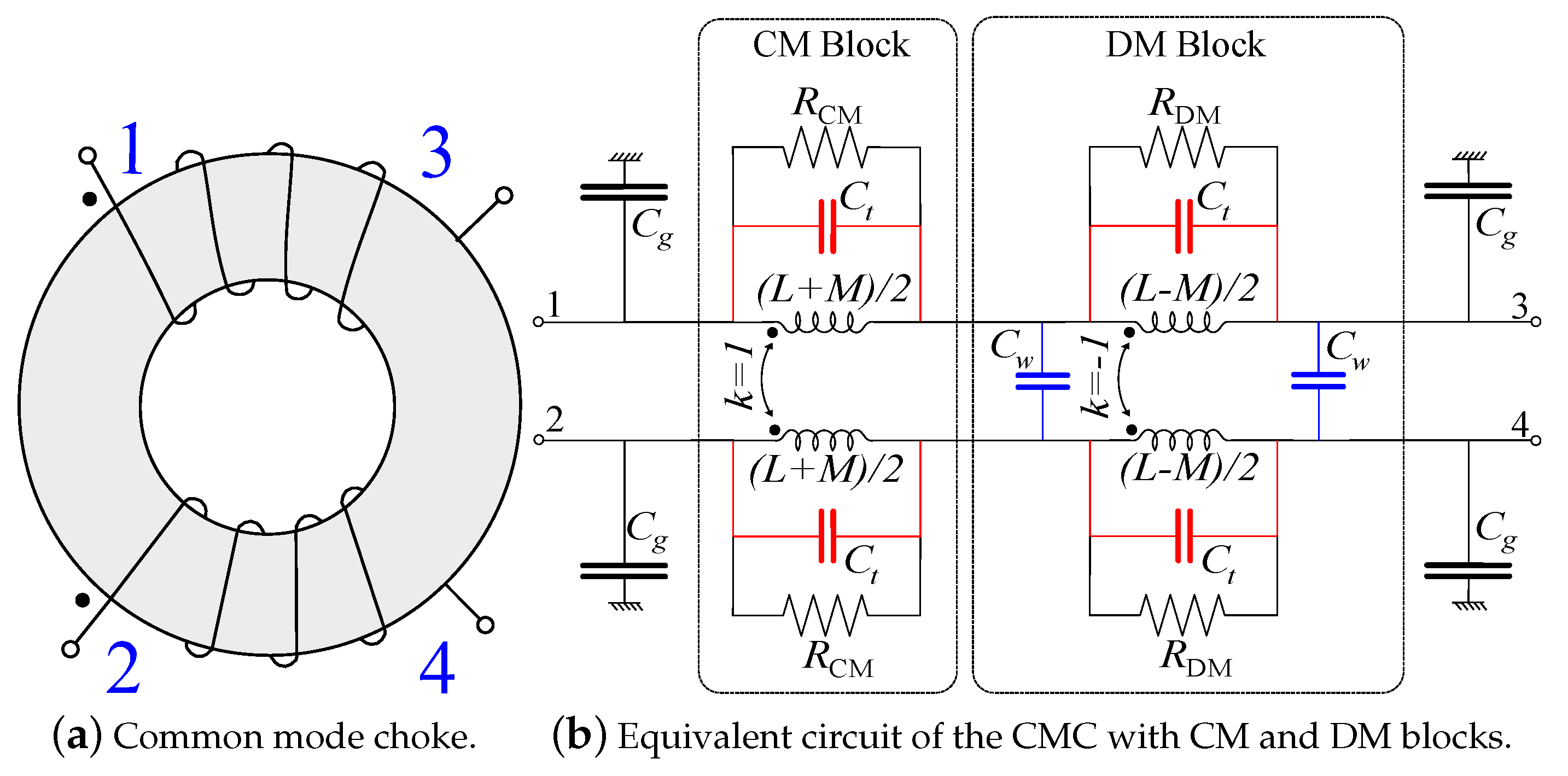
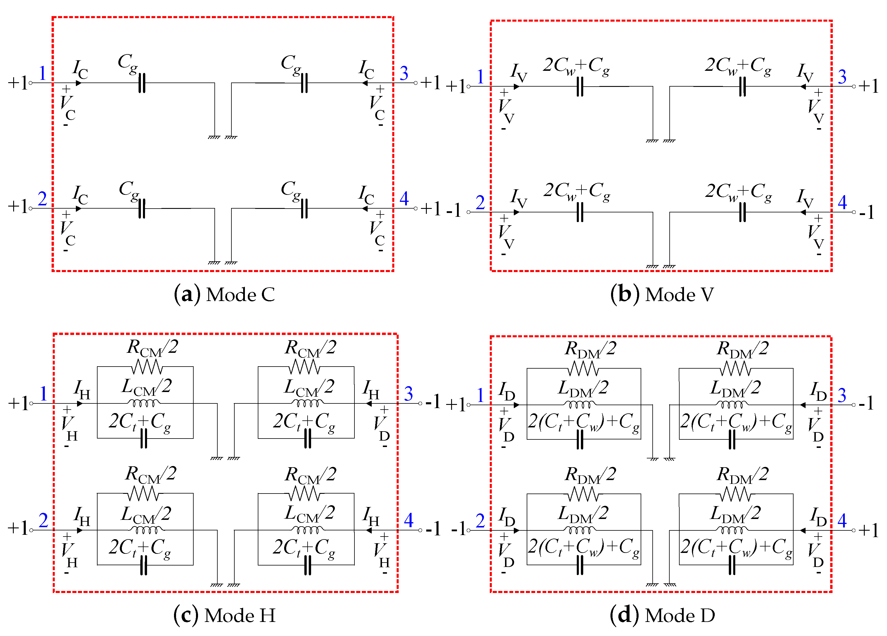
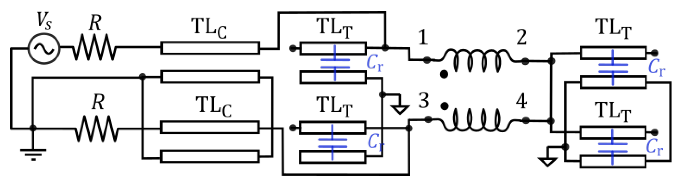
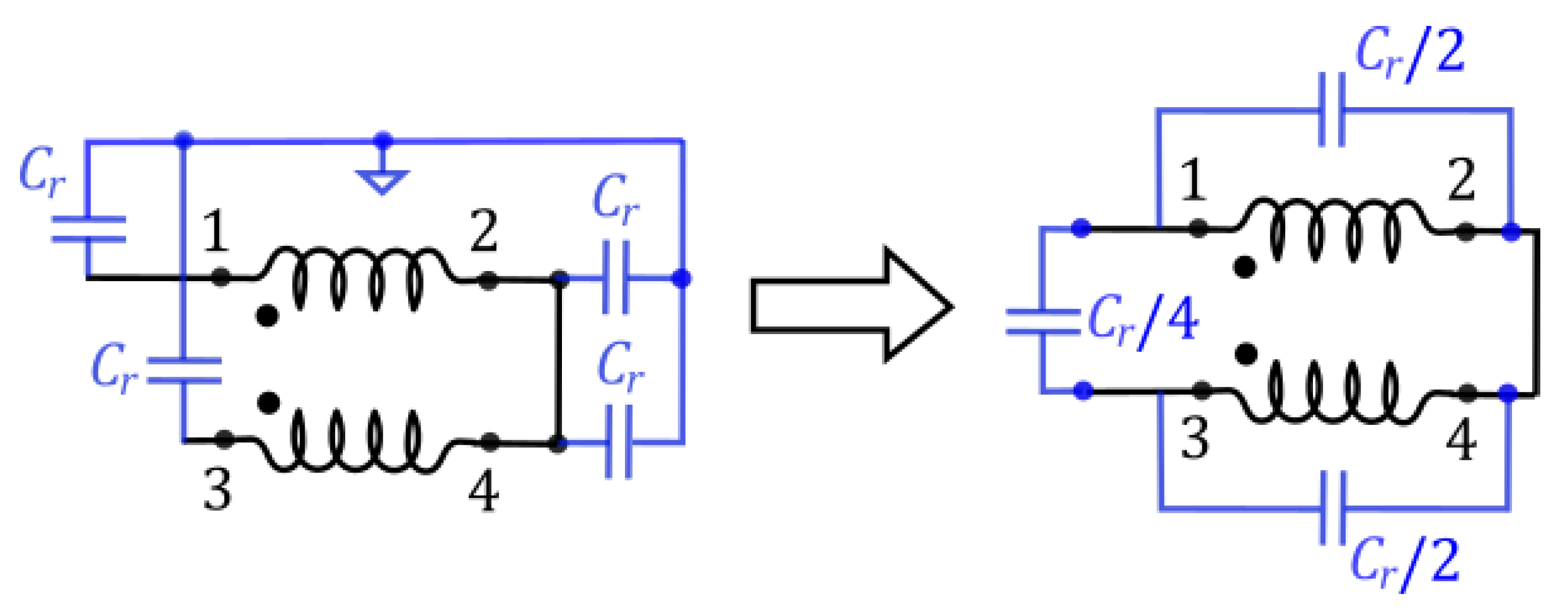
2.1. Modal Analysis of the CMC

The circuit in Figure 1b can be considered to be a four-port network and it can be characterized by a 4×4 admittance matrix [ Y ] . A modal analysis can be carried out by calculating the voltage eigenvectors (modes) that diagonalize [ Y ] , as explained in [16]. In that work, it has been shown that this analysis yields four independent (uncoupled) modes, which are referred to as C, V, H and D modes. In general, for a given excitation of the CMC, its response is always made up of a superposition of the responses of one or more of those natural modes. The equivalent circuits of these four modes are represented in Figure 2. In that figure we also represent the normalized excitation at the four ports of the CMC that corresponds to each mode. Please note that CM and DM excitation of the CMC appear as H and D natural modes of the equivalent circuit of the CMC (Figure 2c,d). As for the other two modes, mode C in Figure 2a corresponds to applying a common voltage to the four ports of the CMC, while mode V in Figure 2b is obtained by applying a difference of voltage between the two windings of the CMC.
In Figure 2 it can be seen that the admittances of the four modes of the CMC are either a capacitive admittance (modes C and V) or the admittance of a resistor, an inductor and a capacitor connected in parallel (parallel RLC circuit), where the inductive component is proportional to L CM = L + M for the CM (H mode) and to L DM = L M (the leakage inductance) for the DM (D mode). The admittances of the four modes of the CMC can be written as follows:
Y C = j ω C g .
Y V = j ω ( 2 C w + C g ) .
Y H = j ω ( 2 C t + C g ) + 2 j ω L CM + 2 R CM .
Y D = j ω ( 2 C t + 2 C w + C g ) + 2 j ω L DM + 2 R DM .
The modal analysis outlined above allows performance of a very efficient analysis of the measurement setups that can be used to characterize the DM response of CMCs. The idea is to express the transmission coefficients corresponding to these measurement setups in terms of the admittances of the natural modes of the CMC to determine to what extent those setups actually excite a pure DM (as intended) and also to assess the impact on measurements of the parasitic effects incorporated to the equivalent circuit of the CMC.
The measurement setup usually required to characterize the DM response of a CMC is schematically shown in Figure 3a [14]. We will refer here to this setup as DM setup. The DM setup requires the use of two baluns (or 180 dividers) to convert the excitation of the output port of the measurement device into a DM signal and to measure the transmitted DM signal at the input port. In other words, the DM setup permits direct measurement of the S DD 21 term of the Mixed-Mode S-Parameter Matrix of the CMC seen as a four-port network [18]. This S DD 21 S-Parameter physically represents the DM response of the CMC to a DM excitation, or equivalently the transmission coefficient (or inverse of the insertion loss) of the DM. For this reason, we will refer here to this S-parameter as S 21 DM . Table 1 provides S 21 DM as a function of the admittances of the natural modes of the CMC. Since only Y D and Y V appear in the expression of S 21 DM , we can conclude that only D (DM) and V modes of the CMC are excited in the DM setup. Also, from that expression it is possible to obtain the frequency of resonance of the CMC in that setup in terms of the elements of the circuit model of the CMC in Figure 1b. This frequency of resonance, f DM , is also given in Table 1 (Since in practice R CM , R DM R = 50 Ω the frequency of resonance can be calculated by taking R CM and R DM in S 21 DM and imposing S 21 DM = 0 ). At frequencies below f DM the response of the CMC is dominated by the inductive part of Y D , i.e., L DM . Above f DM the CMC behaves capacitively and the magnitude of S 21 DM increases with frequency. Please note that since f DM does not depend on C g , an electric coupling to ground will not alter the frequency of resonance of S 21 DM .
As an alternative to the DM setup, in Figure 3b we propose a simpler unbalanced setup (UDM setup) which dispenses with baluns and which at the same time is also able to provide information about the DM response of the CMC. The UDM setup in Figure 3b, like the DM setup in Figure 3a, involves the measurement of a transmission coefficient instead of the measurement of impedances of the CMC. This allows for avoiding additional measurements to account for the effect of cables and/or test fixtures (compensation measurements) [19]. To compare the UDM setup with the DM setup, it is useful to obtain also the transmission coefficient of the UDM setup ( S 21 UDM ) in terms of the admittances of the natural modes of the CMC. An analysis of the circuit in Figure 3b with the circuit model of the CMC in Figure 1b leads to:
S 21 UDM = R ( Y p 4 Y s ) ( 2 + Y p R ) ( 1 + 2 Y s R ) .
where Y p = Y D + Y V + 2 Y C and Y s = Y C Y H / ( Y C + Y H ) . This analysis shows that unlike the DM setup which only excites D and V modes, the UDM setup excites the four natural modes of the CMC. In principle, this makes an important difference between DM and UDM setups. However, it can be easily shown that if measurements are performed avoiding the presence of nearby conducting surfaces, the response of the UDM setup becomes quite similar to that of the DM setup. In particular, only D and V modes are significantly excited in the UDM setup. To demonstrate this, suppose that capacitances to ground are negligible compared with the rest of the capacitances of the circuit model in Figure 1b ( C g C t , C w ). In that case, the expressions for the modal impedances in Equations (1)–(4) allow us to assume that Y C Y V , Y H , Y D . Consequently, we can approximate in (5) Y s Y C Y p Y D + Y V . In that case, a simpler approximation of the expression of S 21 UDM in (5) can be obtained:
S 21 UDM R ( Y D + Y V ) 2 + R ( Y D + Y V ) .
This expression is included in Table 1 along with that of S 21 DM . The frequency of resonance of S 21 UDM in Equation (6) is also provided in that table as f UDM . When comparing S 21 UDM with S 21 DM , it can be noticed that both expressions depend only on Y D and Y V . Moreover, because Y V in Equation (2) is a capacitive admittance related to the inter-winding capacitance, it is expected that at low frequencies Y V Y D and therefore S 21 UDM S 21 DM R Y D / ( 2 + R Y D ) . In other words, at low frequencies (i.e., well below resonance) the response of the CMC is expected to be dominated by L DM and to be the same for the DM setup as for the UDM setup, with currents flowing inside the CMC in a purely differential mode in both cases.
Summing up, the previous analysis demonstrates that provided that coupling with nearby metallic surfaces is negligible, S 21 UDM S 21 DM at low frequencies. This is an important result because it allows us to conclude that at these low frequencies the UDM setup can be used as a simpler alternative to the DM setup to quickly characterize the DM response of a CMC. However, the analysis presented here also demonstrates that at high frequencies some differences should be expected between S 21 DM and S 21 UDM . This will be experimentally checked in Section 3. Before that the next subsections complete the theoretical analysis by analyzing the effect of electric and magnetic couplings of the CMC with nearby conducting surfaces on measurements performed with DM and UDM setups.

2.2. Effect of Electric Coupling to Metallic Surfaces

In the previous section we have seen that the transmission coefficient S 21 DM of the balanced DM setup is inherently independent of Y C (see Table 1) and that electric couplings are not expected to significantly affect measurements carried out with the DM setup. By contrast, external electric couplings will affect measurements with the UDM setup unless S 21 UDM can be approximated by Equation (6). That approximation can be safely applied whenever no metallic surface is allowed near the CMC when measuring. However, there are situations where this cannot be ensured. This may occur for example when measuring a CMC which is mounted on a PCB with a return plane. This PCB can be for example the PCB of the EMI filter or a PCB employed to measure the CMC as a four-port terminal, as required in many cases in the normative [14].
Even for a CMC mounted on a PCB, the return plane is usually sufficiently far from the windings of the CMC as to make it reasonable to disregard a direct electric coupling of the CMC to the return plane with respect to the internal couplings given by the inter-windings and intra-windings capacitances ( C g C t , C w in Figure 1b). However, the effects on the DM and UDM measurements of the microstrip traces of the PCB employed to lead the signals to the four pins of the CMC should be assessed. As for the DM measurements, it can be easily demonstrated that if the characteristic impedance of these signal traces of the PCB are equal to the input and output impedances of the measuring device (usually 50 Ω ), those traces will only introduce a phase shift in the transmission coefficient of the DM setup, but they will not alter the magnitude of S 21 DM [19]. However, the situation is different for the UDM setup.
A schematic of the situation presented for the UDM setup can be seen in Figure 4. That figure represents a CMC connected in the UDM setup, and it includes transmission line models for the interconnecting cables (e.g., coaxial cables), which are labelled as TL C lines, and for the signal traces of the PCB (typically microstrip lines), which are labelled as TL T lines. In principle, TL T traces leading to terminals 1 and 3 of the CMC are not an issue. In fact, provided that they have the same 50 Ω characteristic impedance as TL C lines, those traces will only introduce a phase shift in the transmission coefficient [19]. However, TL T lines attached at terminals 2 and 4 of the CMC create an asymmetric electric coupling of the CMC to ground whose effect is not negligible, as we will show here. To demonstrate that, consider the situation represented in Figure 4, where terminals 2 and 4 of the CMC are directly short-circuited to achieve an UDM configuration that circumvents the two TL T lines attached to those terminals. Considering lengths of TL T lines in the order or centimeters, they will be electrically short at the frequencies of interest and, consequently, these open-circuited lines can be modeled as capacitances [20]. The two parasitic capacitances C r included in Figure 4 account for this effect. Since these C r capacitances correspond to the total capacitance of the trace lines, their values are typically in the order of units or tens of picofarads [20]. Consequently, C r capacitances cannot be disregarded by comparison with typical parasitic capacitances of the CMC, which are of the same order of magnitude.
To investigate the impact on the transmission coefficient measured with the UDM setup of the capacitances C r that must be included in the schematic of the UDM setup in Figure 4, we have calculated the transmission coefficient of that circuit by circuit analysis. We have used the circuit model of the CMC in Figure 1 with Y C = 0 , but we have included the effect of C r capacitors as two external admittances Y R = j ω C r connected to terminals 2 and 4 of the CMC. In this way, we have obtained the following modified S 21 UDM coefficient in terms of the admittances of the modes of the CMC:
S 21 UDM = R ( Y D + Y V ) 2 + R ( Y D + Y V ) R Y HR 2 + R Y HR .
where Y HR = Y H Y R / ( Y H + Y R ) . It is very interesting to note that the only difference between S 21 UDM in (7) and S 21 UDM in Equation (6) is the presence of the second additive term in (7). This term is zero if Y R = 0 ( C r =0), as expected. Therefore, Equation (7) reveals that the effect of considering the electric coupling given by C r is to excite an additional mode of the CMC (H mode), whose admittance Y H acts in series with that of C r . A very good approximation for the frequency of resonance of S 21 UDM in Equation (7) can be obtained if we consider that this frequency must be near that of S 21 UDM , i.e., it must be found at frequencies where ω C t 1 / | ω L DM | . Because in practical CMCs we have L CM L DM , we have 1 / | ω L CM | ω C t and therefore Y H in Equation (3) can be approximated as Y H j ω C t . With this approximation the frequency of resonance of S 21 UDM in Equation (7) can be expressed as:
f UDM = 1 / 2 π ( C t + 2 C w C r C t C r + C t ) L DM .
By comparing this frequency of resonance with f UDM given in Table 1 we conclude that the main effect of C r in the transmission coefficient of the UDM setup is to slightly increase its frequency of resonance.
From the previous analysis we conclude that by contrast with DM setup, the UDM setup is sensitive to the presence of electrical couplings (capacitive effects) caused by the presence of nearby metallic grounded structures such as a ground plane on a PCB, and that this effect can be noticeable at high frequencies.
An interesting question that arises in this point is whether in the UDM setup this effect can be avoided by isolating the return plane of the PCB with respect to ground in the measurement setup. This situation is shown in Figure 5, which represents an alternative implementation of the UDM setup for a CMC mounted on a PCB where the active conductors of the TL C lines (cables) are directly connected to the terminals of the CMC, while circumventing the TL T lines connected to terminals 1 and 3, thus isolating the return plane of the PCB from the ground of the measurement setup. In that case, the four electrically short open-circuited TL T lines connected at each terminal will introduce four parasitic capacitances C r at each terminal of the CMC.
These capacitances connected to a star point (the isolated return plane) can be transformed into its triangle equivalent, as shown in figure Figure 6. That figure shows that the effect of the capacitances C r is to increase the C w parasitic capacitance of the CMC by an amount Δ C w = C r / 4 , and to increase C t by an amount Δ C t = C r / 2 . This should cause a decrease in the frequency of resonance of S 21 UDM with respect to the case with no return plane. Therefore, the UDM Setup will still be sensitive to the presence of the return plane of the PCB. This will be experimentally verified in Section 3.

2.3. Effect of Magnetic Coupling to Metallic Surfaces
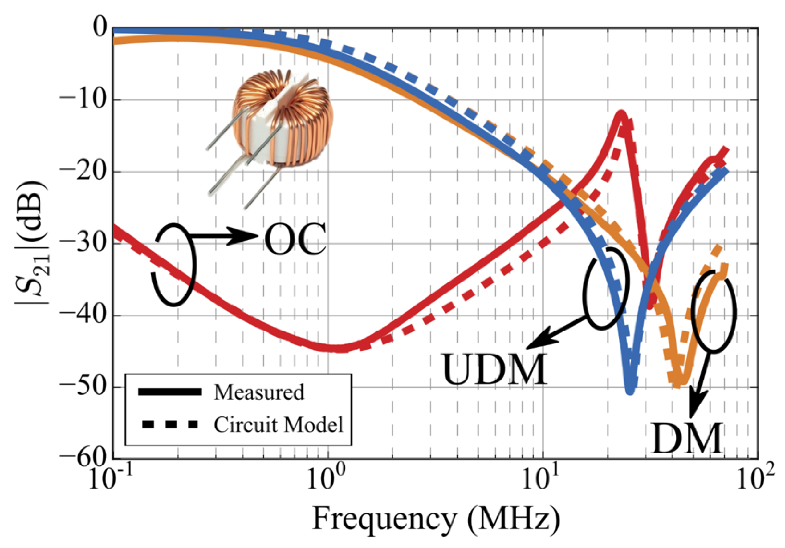
Another effect that can alter the response of a CMC excited by a DM signal is a magnetic coupling of the CMC with nearby metallic surfaces. The root cause of this effect is that, unlike CM currents, DM currents in a CMC create a magnetic field which closes its field lines outside the core of the CMC [21,22]. Therefore, this magnetic field can interact with nearby metallic surfaces such as for instance, the metallic enclosure usually employed for housing and shielding of EMI filters. Even though metallic enclosures are usually constructed with non-magnetic metals, a magnetic coupling might still appear due to eddy currents induced in those conducting surfaces by the time-varying stray magnetic field of the CMC. The effect of these eddy currents is to partially counteract the magnetic fields created by the CMC outside its core, thus causing a decrease of the leakage inductance L DM of the CMC [22,23]. This change of L DM can equally affect measurements performed with the DM or the UDM setups. The actual impact of this effect in practical cases will be investigated in Section 3.3.

3. Results

The analysis presented in the previous section suggests that in principle it is possible to use the UDM setup in Figure 3b to measure the DM response of a CMC. However, since we have shown that electric or magnetic couplings may affect the response of the CMC, the impact of these effects on measurements performed with the UDM setup must be assessed to clearly determine the scope and limitations of this method of measurement by comparison with standard DM measurement. To this end, we present in this section experimental results for several commercial CMCs in different setups. These measurements have been carried out by using a Rhode&Schwarz ZND VNA. However, note that measurements of the magnitude of a transmission coefficient can be alternatively performed by using a spectrum analyzer with tracking generator.

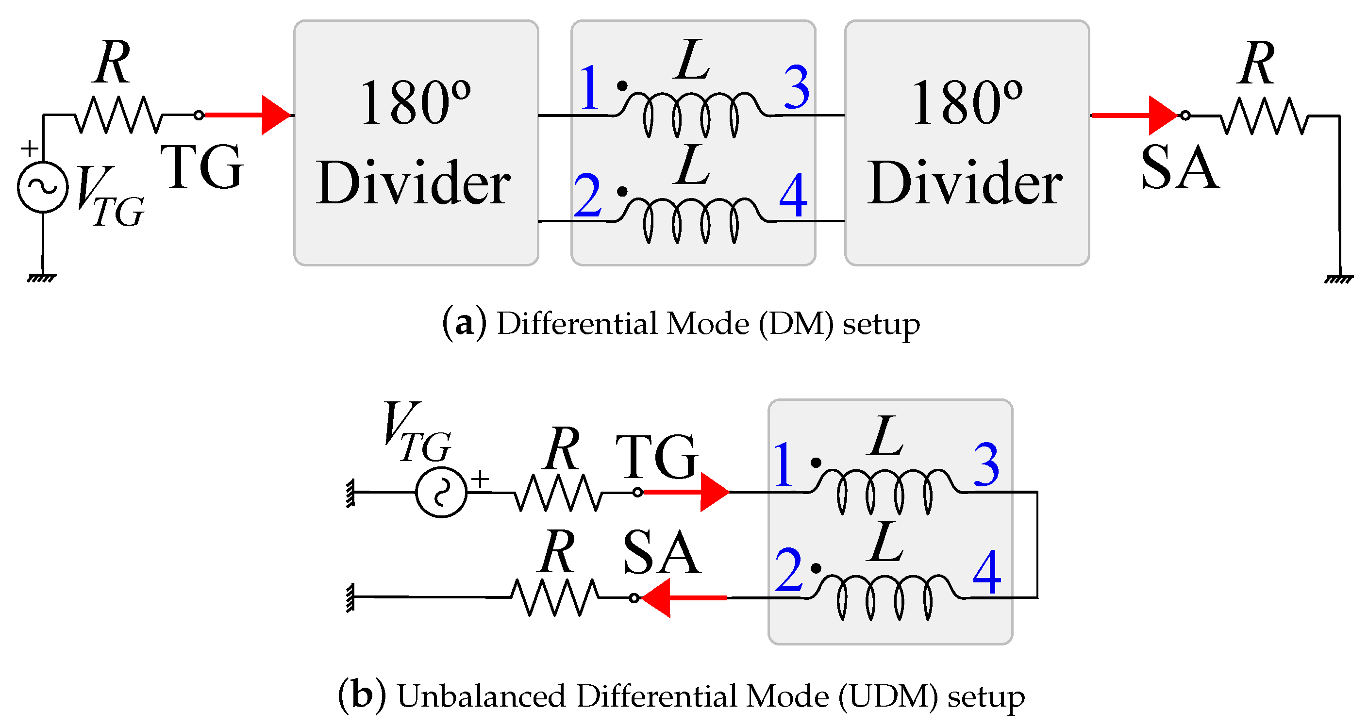
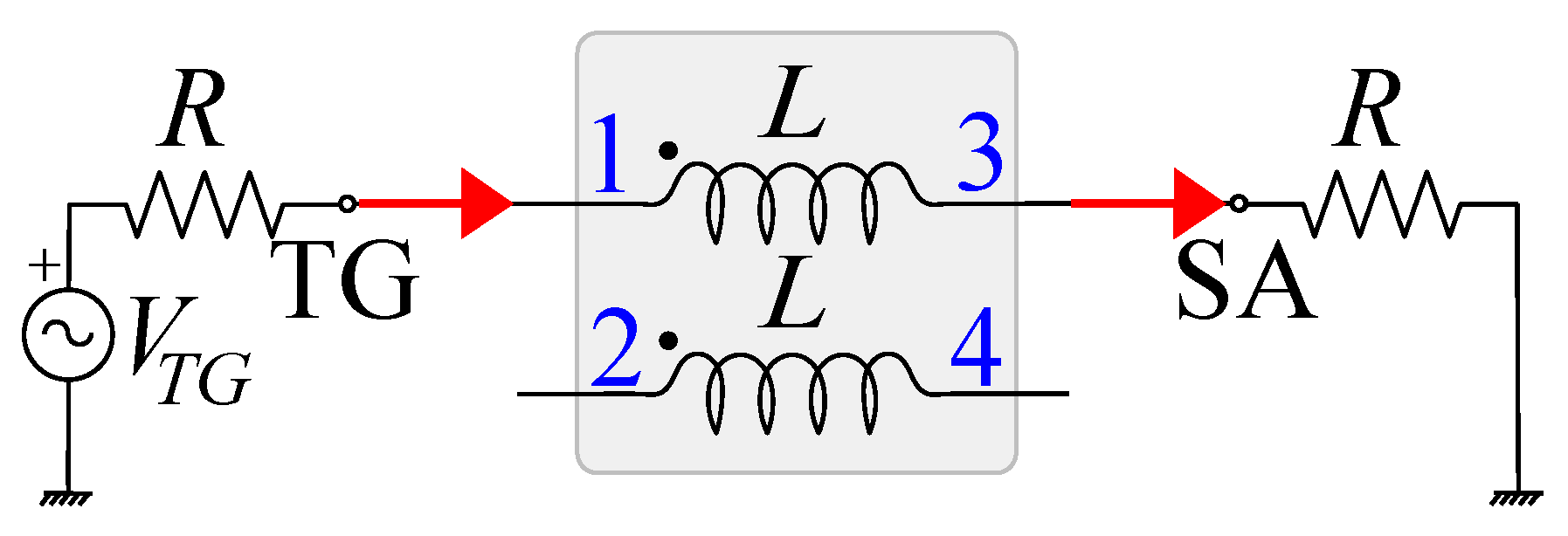
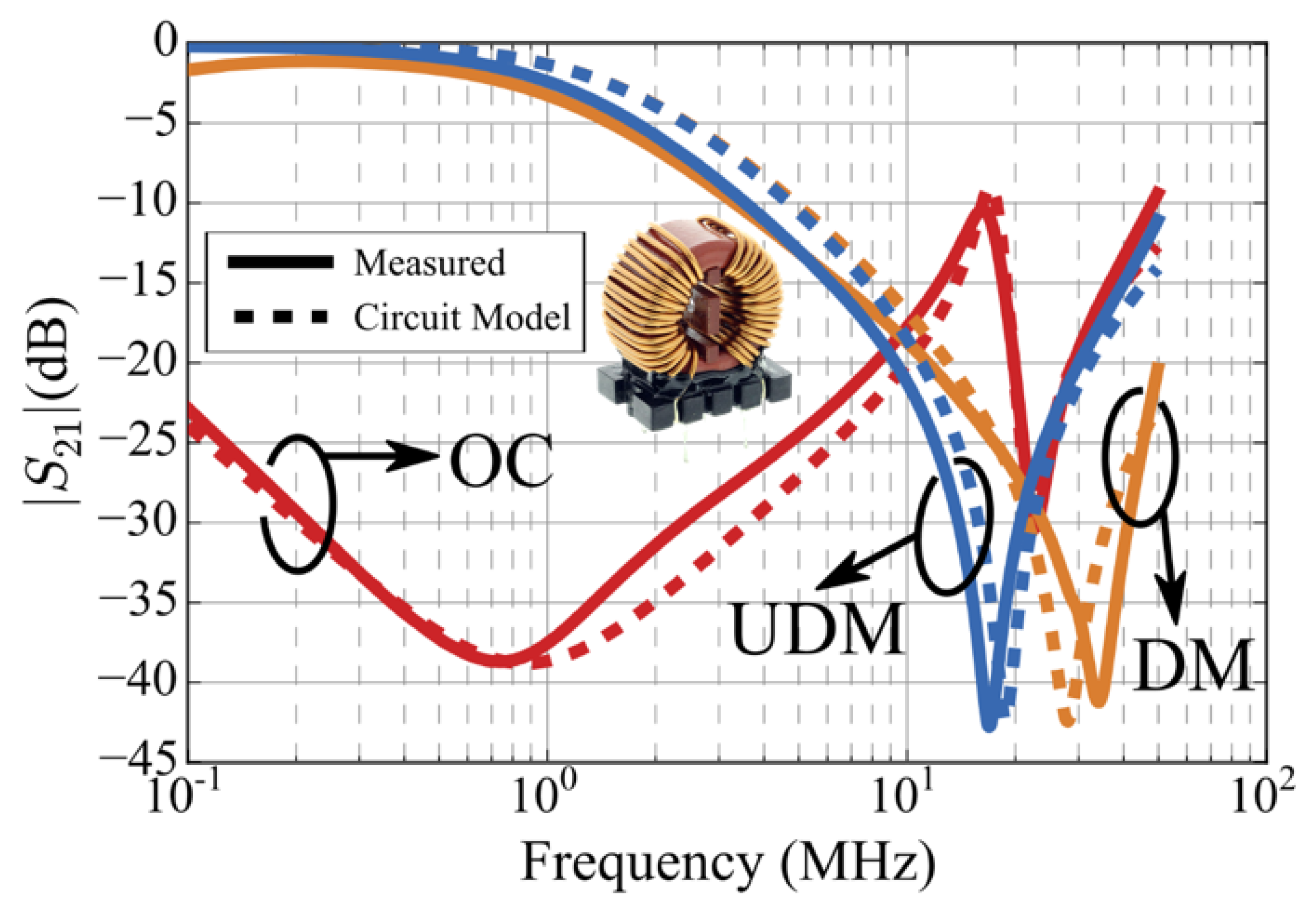
3.1. Analysis of the Response of a Standalone CMC

To validate the analysis presented in Section 2 we have measured the response of the CMCs listed in Table 2 in the DM and UDM setups shown in Figure 3. Also, we have used an alternative setup, referred to as Open-Circuit (OC) setup, which is shown in Figure 7. This setup was proposed in [16] to characterize CMCs. The main difference between OC setup and UDM is that since the OC setup is actually used for obtaining a complete circuit model of the CMC and it is not conceived as a measurement method to characterize its DM response, in the OC setup both the CM (H) and DM (D) modes of the CMC are simultaneously excited. An expression for the transmission coefficient of the CMC in the OC setup, S 21 OC in terms of Y H and Y D is given in Table 1 [16]. From this expression, it can be easily demonstrated that S 21 OC always presents two frequencies of resonance: one related to L CM and another one at a higher frequency associated with L DM which is given in Table 1 as f OC . As a consequence of this double resonance, the OC setup does not allow quick measurement of the response of a CMC to a purely DM signal throughout the entire range of frequencies of interest. However, since the expression and physical meaning of f OC has been previously studied in [16], we will use it here to validate our analysis of the UDM setup as explained below.
By comparing the frequencies of resonance in Table 1 it is apparent that for a given CMC we must have f UDM < f OC < f DM . We will use here this fact to verify the accuracy of our circuit model and to check the expressions for the transmission coefficients of the DM and UDM setups, S 21 DM and S 21 UDM , presented in Table 1.
Figure 8 shows | S 21 DM | , | S 21 UDM | and | S 21 OC | measured for the CMC listed as WÜRTH ELEKTRONIK 744824622 (2.2 mH) in Table 2. It can be observed that each one of these curves present a resonance dip related to differential excitation of the CMC, as expected. Also, note that these frequencies of resonance are different for the three setups. In fact, resonance occurs first for the UDM setup, then for the OC setup (second resonance) and finally, for the DM, i.e., f UDM < f OC < f DM . These results are consistent with our previous analysis. Similar results are obtained for all the CMCs in Table 2. An additional example is represented in Figure 9 for another CMC, identified in the caption of the figure and listed in Table 2.
To further ensure consistency of the measured curves with our theoretical analysis, we have used an advanced search algorithm based upon genetic algorithms (GA) [24] to find a set of values for the components of the circuit in Figure 1b that allow us to simultaneously fit the measured S 21 OC and S 21 DM curves. Parameters obtained for all the CMCs analyzed here are given in Table 2. Then, we have used these circuit parameters to calculate | S 21 UDM | using the expression given in Table 1. These curves are represented in Figure 8 and Figure 9 as dashed lines, and labelled as calculated results. A good agreement between measured and calculated results can be observed in these graphs. Similar results are obtained for all the CMCs in Table 2. This permits us to ensure that the high-frequency circuit model in Figure 1b is reasonably accurate within the range of frequencies where most EMC regulations impose limits to conducted emissions [25,26,27].
It is worth pointing out that in the measurements performed in this section external magnetic or electric couplings have been carefully avoided by keeping the CMC under test far from metallic surfaces (a distance greater than the size of the CMC is typically enough). This is important because the expression for S 21 OC in Table 1, such as that of S 21 UDM Equation (6), assumes that parasitic capacitances to ground can be disregarded, i.e., Y C Y V , Y H , Y D . The effect on measurements of electric coupling with nearby metallic surfaces will be analyzed in the next subsection.

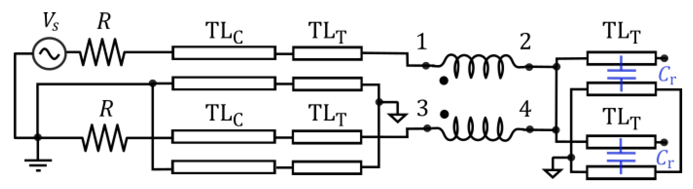
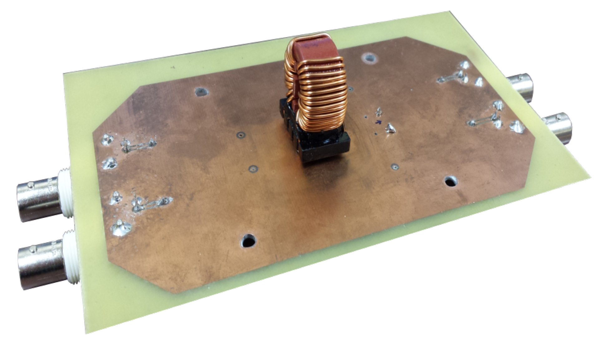
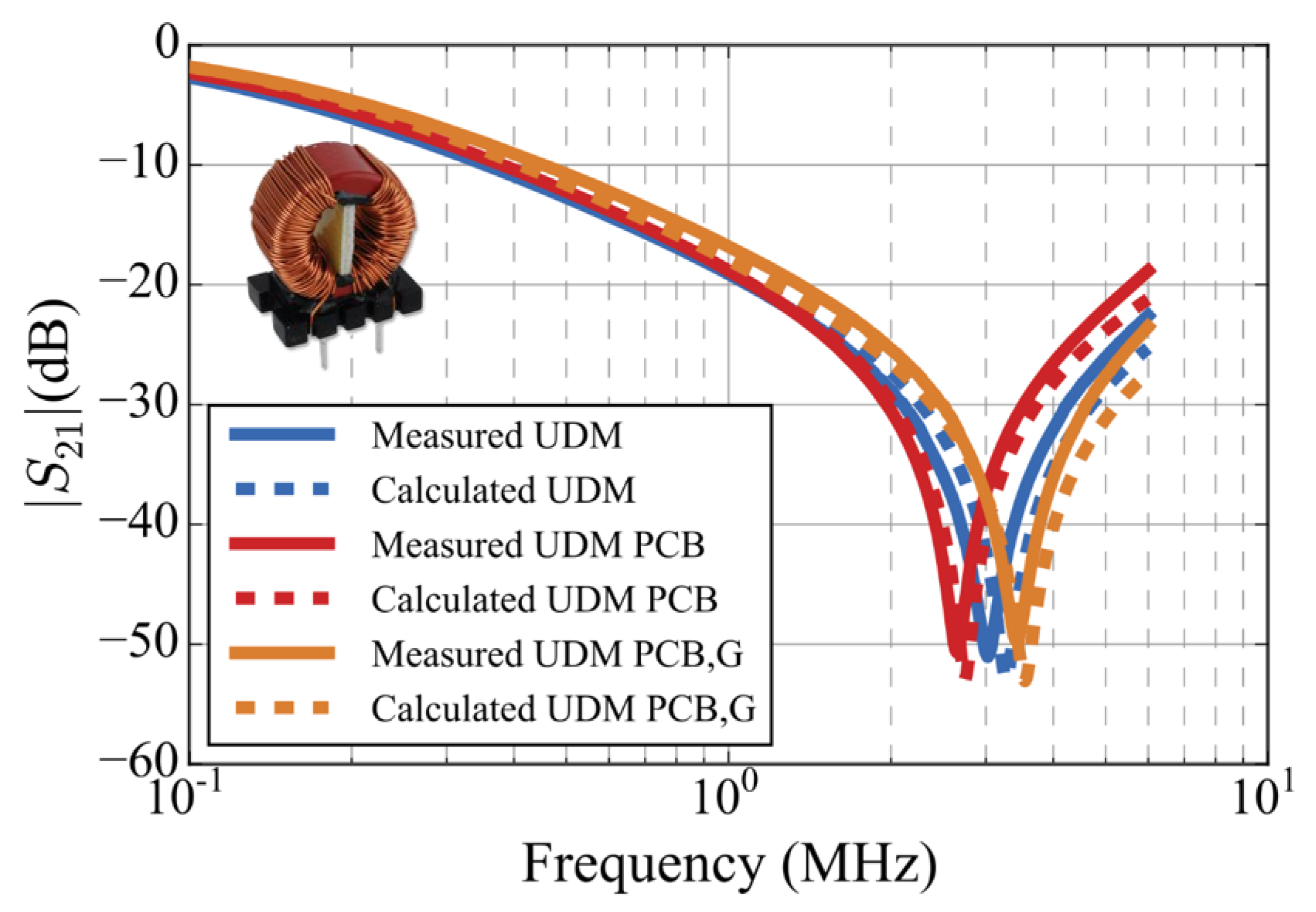
3.2. Effect of Capacitive Couplings in a PCB

The analysis presented in Section 2.2 shows that when a CMC is mounted on a PCB (a situation that may easily arise in practice), the parasitic capacitances introduced by the traces connected to the terminals of the CMC might alter the measurements of S 21 UDM , thus rendering misleading results if the aim is to characterize the CMC as a standalone component. In this section, we will analyze the actual impact of this effect by comparing measured S 21 UDM for an isolated CMC with results obtained when the CMC is mounted on a PCB representative of those usually employed to fabricate EMI filters.
Figure 10 shows a CMC mounted on a PCB fabricated with a 1.5 mm-thick FR4 substrate. Signal traces (not visible in Figure 10 because the CMC is mounted on the side of the return plane) are 4 mm-width×60 mm-long strips connecting the CMC pins to the BNC connectors. These signal traces, along with the BNC connectors, add an extra parasitic capacitance between the four ports of the CMC and the return plane (RP). We have measured this parasitic capacitance, obtaining a value of C r = 17.5 pF.
As a first step, we have checked that the fact that the CMC is mounted on a PCB has a negligible effect on the measurements of | S 21 DM | , as expected from the analysis in Section 2. This robustness of S 21 DM measurements against external electric couplings comes from the balanced nature of this setup, and represents an advantage of this measurement technique. On the contrary, and according to the analysis in Section 2.2, the measure of | S 21 UDM | could be affected by the parasitic capacitances appearing at the terminals of the CMC when it is mounted on a PCB with a RP. To study the actual impact of this effect in a practical case, Figure 11 shows | S 21 UDM | measured for the CMC listed as WÜRTH ELEKTRONIK 744824220 (20 mH) in Table 2 in three different situations: when CMC is isolated (no magnetic or electric coupling with nearby conducting surfaces), when CMC is mounted in the PCB but the RP is not grounded (schematic in Figure 4) and finally, when the CMC is mounted in the PCB and the RP is grounded (schematic in Figure 5). Curves in Figure 11 show that the response of the CMC at low frequencies (well below resonance) is the same for these three situations. However, Figure 11 also reveals that at high frequencies there exists a shift in the frequency of resonance of S 21 UDM . Compared to the isolated case, the frequency of resonance is slightly lower when the RP is not grounded and slightly higher when the RP is grounded. These results are consistent with the analysis presented in Section 2.2. We have obtained similar results for all the CMCs in Table 2.
To analyze this effect in more detail, and also to check the explanation provided inSSection 2.2, we have measured the frequencies of resonance of three different CMCs (among those in Table 2) when measured in the three different situations described above. In Table 3 we compare the frequency of resonance measured with the CMC isolated with that obtained when the CMC is placed on a PCB with an ungrounded RP. Those results show that the effect of the presence of the isolated RP is to decrease the frequency of resonance of S 21 UDM by an amount that goes from 10% to 20%. Table 3 also includes for each CMC the frequency of resonance calculated by using the expression of f UDM given in Table 1, where C t and C w have been modified to C t = C t + C r / 2 and C w = C w + C r / 4 in accordance with the results of the analysis presented in Section 2.2. The rest of the parameters of the model of each CMC have been taken from Table 2. Results in Table 3 show that the calculated frequency of resonance agrees reasonably well with the measured one, with typical discrepancies around 5%. This allows us to conclude that the decrease of the frequency of resonance of S 21 UDM observed when the CMC is mounted on a PCB with an isolated RP is mainly caused by the parasitic capacitances between the traces and the isolated return plane of the PCB.
Table 4 compares the frequency of resonance of S 21 UDM measured when the CMC is isolated with that measured when the CMC is mounted on a grounded PCB for the same three CMCs listed in Table 3. Results show that the grounded RP causes the frequency of resonance to increase in all the cases, as expected. This increase is up to 35% for the WE 2.2 mH CMC. Frequencies of resonance f UDM calculated by using (8) are also included in Table 4. The good agreement found in general between calculated and measured results confirms that the shift of the frequency of resonance of S 21 UDM is caused by the presence of the grounded RP and that this shift can be approximately predicted by using Equation (8).
Summing up, results in this section show that when measured in the UDM setup, the capacitance between the signal traces and the RP of the PCB can modify the response of the CMC at high frequencies. Therefore, when accurate results are required, measuring a CMC mounted on a PCB with the UDM setup should be avoided unless the effect of the parasitic capacitances of the signal traces to the RP is accounted for.
Another interesting conclusion that can be obtained from these results refers to the impact of magnetic coupling. Figure 11 shows that at low frequencies the response of the standalone CMC coincides with those measured when the CMC is mounted on a PCB. Therefore, we can conclude that at low frequencies (i.e., well below resonance), the RP has no significant effect on L DM . This is because the RP is not sufficiently close to the windings of the CMC. Situations where magnetic coupling with external metallic surfaces may have an impact on the measurements of S 21 UDM (and S 21 DM ) will be analyzed in the next subsection.

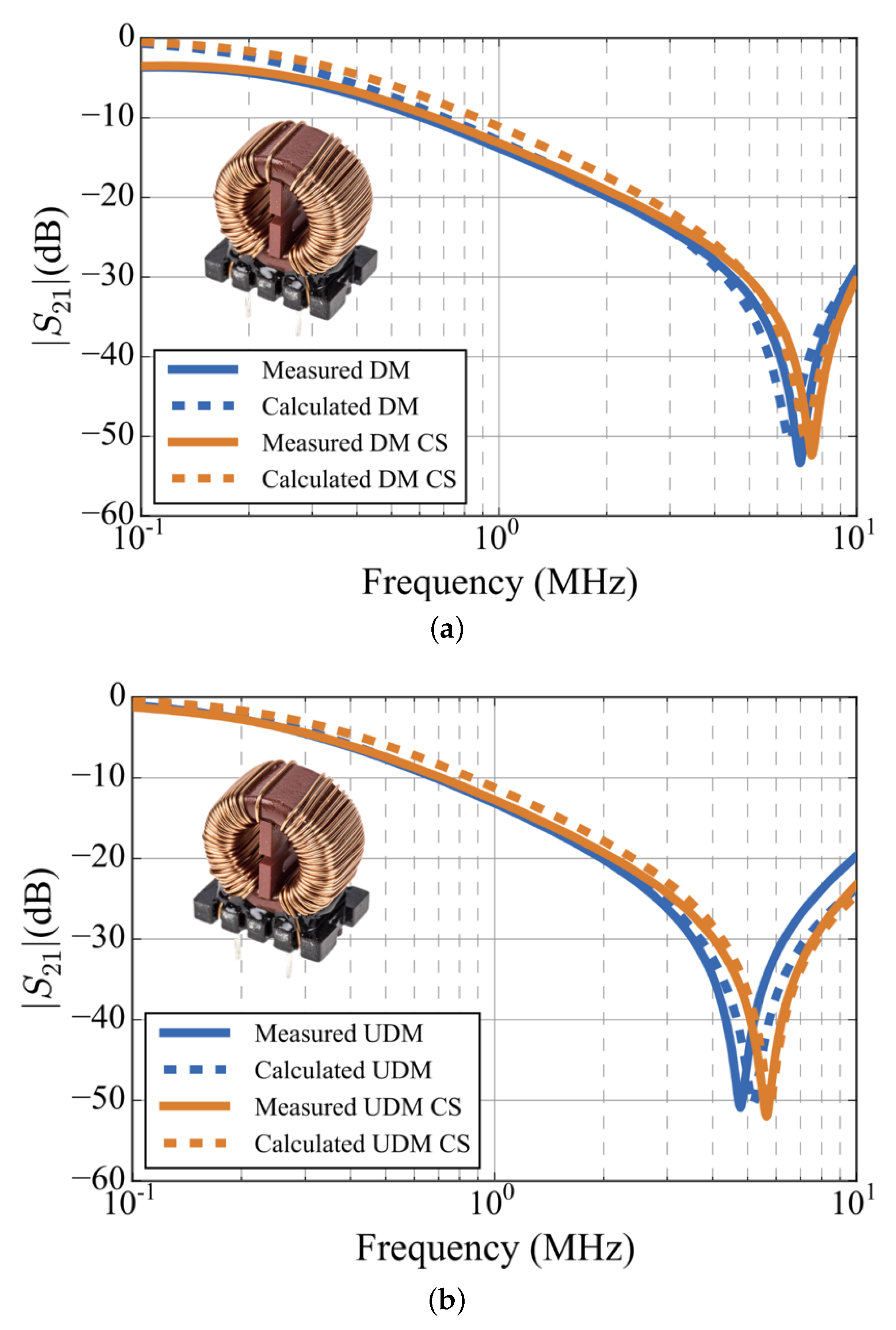
3.3. Effect of Magnetic Coupling to Nearby Conducting Surfaces

The aim of this section is to study the sensitivity of the measurements of S 21 DM and S 21 UDM to the effect of magnetic coupling to nearby conducting surfaces (CS). We have verified for all the CMCs in Table 2 that the measurements of S 21 DM and S 21 UDM are altered by the presence of an isolated (i.e., not necessarily grounded) copper plate placed very close to the top of the CMC. This situation is representative of that that may arise in practice when the CMC of an EMI filter is placed very close to the metallic enclosure of the filter. We have verified that this effect is noticeable only if the CS is very close to the windings (in general, less than 1mm apart). In fact, we have checked that the effect of magnetic coupling is very weak when the CS is placed beneath (instead of on top) of the CMC, because in this case the leads and the plastic structure that typically supports the CMC keep the CS sufficiently far from the windings of the CMC to prevent a significant magnetic coupling. This is consistent with results for CMCs mounted on a PCB presented in the previous section, where we have seen that the effect of the return plane of the PCB on the leakage inductance of the CMC, L DM , is negligible.
As an example to show the effect of magnetic coupling on the DM response of CMCs, we represent in Figure 12 the measured | S 21 UDM | and | S 21 DM | with and without the presence of a CS for the 10 mH CMC listed as WÜRTH ELEKTRONIK 744824310 in Table 2. The CS employed to induce magnetic coupling in this experiment is a 10cm-side square copper plate which has been placed on top of the CMC, only separated by a paper film whose thickness is approximately 0.1 mm. Figure 12 shows that the effect of the CS is to slightly increase both | S 21 DM | and | S 21 UDM | at low frequencies and also to increase their respective frequencies of resonance. These effects can be explained by a decrease of L DM . To demonstrate this, we have included in Figure 12 the | S 21 DM | and | S 21 UDM | curves calculated by using the equivalent circuit of Figure 1b with the parameters extracted in the previous sections (Table 2) and also the same curves obtained after conveniently decreasing L DM . Those calculated results agree very well with measurements. In general, the effect of the magnetic coupling created by CS placed very close to a CMC is to decrease the leakage inductance of the CMC by an amount between a 20% and a 30%. Detailed quantitative results are provided in Table 5 for the CMC in Figure 12 and two additional CMCs among those listed in Table 2. Table 5 compares for each CMC the inductance L DM calculated without the presence of a CS with the reduced inductance (referred to as L DM CS ) that should be used to match the S 21 DM and S 21 UDM curves in the presence of a CS. It is interesting to highlight that the same reduced inductance L DM CS can be used to account for the effect of the magnetic coupling for both the DM and UDM measurements, as should be expected.
The main conclusion that can be drawn from the experiment described in this section is that a closely placed CS can alter the DM response of a CMC by decreasing its leakage inductance. Moreover, this effect can equally affect measurements in both the DM and the UDM setups. This implies that independently of the setup, magnetic coupling should be avoided (by keeping the CMC sufficiently far apart from metallic surfaces) to prevent an inaccurate characterization of the DM response of a CMC as a standalone component. Alternatively, in case the actual metallic enclosure where the CMC is going to be placed is available, it would be possible to determine its effect on the leakage inductance of a CMC by measuring it in the UDM setup with the CMC placed in the same relative position with respect to the metallic enclosure that it is intended to occupy in practice.
From results in Figure 12, it is also interesting to note that below approximately 3 MHz, | S 21 DM | curves coincide very well with | S 21 UDM | ones. This is consistent with the discussion presented in Section 2.1, where we demonstrate that at low frequencies the response of a CMC is mainly determined by L DM and that is expected that S 21 DM S 21 UDM . This confirms that in the range of frequencies where the CMC behaves inductively, the UDM setup can be effectively used to predict the DM insertion loss of a CMC.
It is also worth pointing out that the curves for | S 21 DM | in Figure 12a show a slight attenuation at very low frequencies (between 100 kHz and 200 kHz) when compared with | S 21 UDM | curves in Figure 12b. This effect can also be observed in measured | S 21 DM | represented in Figure 8 and Figure 9. We have verified that this is caused by a decrease in the performance of the baluns that we have employed in these measurements, due to its limited bandwidth (We have used baluns constructed with commercial wide-band 1:1 transformers Coilcraft WB2010-1 [28].). Although this problem could be solved by using baluns with a wider bandwidth or by performing a careful calibration, we point it out here to highlight an inherent shortcoming of the DM setup, namely its dependence on ancillary circuitry whose effect on the measurements has to be carefully taken into account.

4. Discussion and Conclusions

This work presented a thorough analysis of a measurement setup, referred to as UDM setup, which can be used to readily measure the response of a CMC to DM signals throughout the frequency range where most EMC regulations impose limits to conducted emissions. The UDM setup is conceived as a simpler and faster alternative to balanced setups, which require ancillary circuits (baluns), and to the use of sophisticated equipment such as four-port VNAs.
We have presented a detailed analysis of the UDM setup based on a modal analysis of a high-frequency circuit model of the CMC. This modal analysis has allowed us to obtain analytical expressions for the transmission coefficients of the CMC in terms of the admittances of the natural modes of the CMC, both for the DM and UDM setups. From these expressions it has been possible to determine the modes actually excited in the CMC in each setup which has permitted us to analyze the effect of parasitic effects on each setup and to identify the conditions that ensure similar responses of the CMC for the DM and UDM measurement setups.
The analysis and experimental results presented in this work provide a deep understanding on the differences and similarities between both techniques of measurement. This has allowed us to demonstrate that the DM setups is inherently immune to (symmetric) external electric coupling while the UDM is sensitive to this effect. By contrast, we have verified that both DM and UDM setups are equally sensitive to magnetic coupling of the CMC to nearby conducting surfaces because this effect modifies the leakage inductance of the CMC. We have quantified the impact of these effects in some practical cases and we have found that provided that the presence of nearby conducting surfaces is avoided or carefully accounted for, the proposed UDM setup can be used to assess the response of a CMC to DM noise within a range of frequencies of practical interest.
Summing up, the main contribution of the present work is to provide a deep understanding on the actual scope and limitations of a simple technique that can be used to measure the attenuation provided by a common mode choke to differential mode signals. This is important because the simplicity of the proposed measurement technique makes it very appropriate for quick assessment of the suitability of a common mode choke for a particular application. In fact, the quick assessing of the impedance and DM attenuation of a CMC provided by the proposed measurement approach facilitates the tasks of ensuring stability and compliance of electronic equipment with conducted emissions limits imposed by EMC regulations.

Author Contributions

Conceptualization, J.B.-M. and M.A.M.-P.; methodology, J.B.-M.; software, C.D.-P.; validation, P.G.-V. and C.D.-P.; formal analysis, P.G.-V. and C.D.-P.; investigation, P.G.-V. and C.D.-P.; resources, M.A.M.-P.; data curation, C.D.-P.; writing–original draft preparation, J.B.-M. and P.G.-V.; writing–review and editing, J.B.-M. and M.A.M.-P.; visualization, C.D.-P. and P.G.-V.; supervision, M.A.M.-P. and J.B.-M.; project administration, M.A.M.-P.; funding acquisition, J.B.-M. and M.A.M.-P. All authors have read and agreed to the published version of the manuscript.

Funding

This work has been supported by the Spanish Ministerio de Economía y Competitividad (project TEC2014-54097-R) and by H2020-EU.3.4.5.6. SCOPUS project (Grant agreement ID: 831942).

Conflicts of Interest

The authors declare no conflict of interest.

References

  1. Kovacevic, I.F.; Friedli, T.; Muesing, A.M.; Kolar, J.W. 3-D electromagnetic modeling of EMI input filters. IEEE Trans. Ind. Electron. 2014, 61, 231–242. [Google Scholar] [CrossRef]
  2. Paul, C.R. Introduction to Electromagnetic Compatibility; John Wiley and Sons: Hoboken, NJ, USA, 2006. [Google Scholar]
  3. Wang, S.; Lee, F.; Chen, D.; Odendaal, W. Effects of parasitic parameters on EMI filter performance. IEEE Trans. Power Electron. 2004, 19, 869–877. [Google Scholar] [CrossRef]
  4. Wang, S.; Chen, R.; Van Wyk, J.D.; Lee, F.C.; Odendaal, W.G. Developing parasitic cancellation technologies to improve EMI filter performance for switching mode power supplies. IEEE Trans. Electromagn. Compat. 2005, 47, 921–929. [Google Scholar] [CrossRef]
  5. Chiu, H.J.; Pan, T.F.; Yao, C.J.; Lo, Y.K. Automatic EMI measurement and filter design system for telecom power supplies. IEEE Trans. Instrum. Meas. 2007, 56, 2254–2261. [Google Scholar] [CrossRef]
  6. Kotny, J.L.; Margueron, X.; Idir, N. High-frequency model of the coupled inductors used in EMI filters. IEEE Trans. Power Electron. 2012, 27, 2805–2812. [Google Scholar] [CrossRef]
  7. Baccigalupi, A.; Daponte, P.; Grimaldi, D. On a circuit theory approach to evaluate the stray capacitances of two coupled inductors. IEEE Trans. Instrum. Meas. 1994, 43, 774–776. [Google Scholar] [CrossRef]
  8. Cogitore, B.; Keradec, J.; Barbaroux, J. The two-winding transformer: An experimental method to obtain a wide frequency range equivalent circuit. IEEE Trans. Instrum. Meas. 1994, 43, 364–371. [Google Scholar] [CrossRef]
  9. Schellmanns, A.; Berrouche, K.; Keradec, J.P. Multiwinding transformers: A successive refinement method to characterize a general equivalent circuit. IEEE Trans. Instrum. Meas. 1998, 47, 1316–1321. [Google Scholar] [CrossRef]
  10. Margueron, X.; Keradec, J.P. Identifying the magnetic part of the equivalent circuit of n-winding transformers. IEEE Trans. Instrum. Meas. 2007, 56, 146–152. [Google Scholar] [CrossRef]
  11. Besri, A.; Chazal, H.; Keradec, J.P. Capacitive behavior of HF power transformers: global approach to draw robust equivalent circuits and experimental characterization. In Proceedings of the 2009 IEEE Instrumentation and Measurement Technology Conference, Singapore, 5–7 May 2009; pp. 1262–1267. [Google Scholar]
  12. Roc’h, A.; Bergsma, H.; Zhao, D.; Ferreira, B.; Leferink, F. A new behavioural model for performance evaluation of common mode chokes. In Proceedings of the 2007 18th International Zurich Symposium on Electromagnetic Compatibility, Munich, Germany, 24–28 September 2007; pp. 501–504. [Google Scholar]
  13. Stevanovic, I.; Skibin, S.; Masti, M.; Laitinen, M. Behavioral modeling of chokes for EMI simulations in power electronics. IEEE Trans. Power Electron. 2013, 28, 695–705. [Google Scholar] [CrossRef] [Green Version]
  14. CISPR 17:2011. Methods of Measurement of the Suppression Characteristics of Passive EMC Filtering Devices; IEC: Geneve, Switezerland, 2011. [Google Scholar]
  15. Kyyrä, J.; Kostov, K. Insertion loss in terms of four-port network parameters. IET Sci. Meas. Technol. 2009, 3, 208–216. [Google Scholar]
  16. Dominguez-Palacios, C.; Bernal-Méndez, J.; Martin Prats, M.A. Characterization of common mode chokes at high frequencies with simple measurements. IEEE Trans. Power Electron. 2018, 33, 3975–3987. [Google Scholar] [CrossRef] [Green Version]
  17. Den Bossche, A.V.; Valchev, V.C. Inductors and Transformers for Power Electronics; CRC Press: Boca Raton, FL, USA, 2005. [Google Scholar]
  18. Bockelman, D.E.; Eisenstadt, W.R. Combined differential and common-mode scattering parameters: Theory and simulation. IEEE Trans. Microw. Theory Technol. 1995, 43, 1530–1539. [Google Scholar] [CrossRef] [Green Version]
  19. Bernal-Méndez, J.; Freire, M.J.; Martin Prats, M.A. Overcoming the effect of test fixtures on the measurement of parasitics of capacitors and inductors. IEEE Trans. Power Electron. 2020, 35, 15–19. [Google Scholar] [CrossRef]
  20. Pozar, D. Microwave Engineering; Wiley&Son: Hoboken, NJ, USA, 2011. [Google Scholar]
  21. Nave, M. Power Line Filter Design for Switched-Mode Power Supplies; Van Nostrand Reinhold: New York, NY, USA, 1991. [Google Scholar]
  22. Dominguez Palacios, C.; Gonzalez Vizuete, P.; Martin Prats, M.A.; Bernal, J. Smart shielding techniques for common mode chokes in EMI filters. IEEE Trans. Electromagn. Compat. 2019, 61, 1329–1336. [Google Scholar] [CrossRef]
  23. Bernal-Méndez, J.; Freire, M.J. On-site, quick and cost-effective techniques for improving the performance of EMI filters by using conducting bands. In Proceedings of the 2016 IEEE International Symposium on Electromagnetic Compatibility, Ottawa, ON, Canada, 25–29 July 2016; pp. 390–395. [Google Scholar]
  24. Weile, D.; Michielssen, E. Genetic algorithm optimization applied to electromagnetics: A review. IEEE Trans. Antennas Propag. 1997, 45, 343–353. [Google Scholar] [CrossRef]
  25. EN55011:2011/CISPR 11. Industrial, Scientific, and Medical Equipment—Radio-Frequency Disturbance Characteristics—Limits and Methods of Measurement; Beuth Verlag: Berlin, Germany, 2009. [Google Scholar]
  26. EN55022:2011/CISPR 22. Information Technology Equipment—Radio disturbance characteristics—Limits and methods of measurement; Beuth Verlag: Berlin, Germany, 2008. [Google Scholar]
  27. FCC Part 15. The FCC 47 CFR Part 15 from the Federal Communications Commission: Rules and Regulations for EMC; Federal Communications Commission: Washington, DC, USA, 2020.
  28. Available online: https://www.coilcraft.com/wbt.cfm (accessed on 15 March 2012).
Figure 1. Representation and circuit model of a common mode choke made up of two equal coupled windings with self-inductance L and mutual inductance M.
Electronics 09 00381 g001
Figure 2. Equivalent circuits of the modes obtained for the high-frequency circuit of the CMC in Figure 1b. Normalized voltages at the four terminals of the CMC are indicated for each mode.
Electronics 09 00381 g002
Figure 3. Balanced and unbalanced setups for measuring transmission coefficients conveying information about the attenuation provided by a CMC for a differential mode excitation. Measurements can be performed with a spectrum analyzer (SA) with tracking generator (TG) or a VNA.
Electronics 09 00381 g003
Figure 4. Schematic of a CMC mounted on a grounded PCB connected in UDM setup. Transmission lines labelled as TL C stand for the interconnecting cables. Transmission lines labelled as TL T represent the signal traces of the PCB. The signal traces terminated as open-circuits at terminals 2 and 4 are supposed to be electrically short and thereby modeled as two capacitances C r to ground.
Electronics 09 00381 g004
Figure 5. Equivalent circuit of the UDM setup for a CMC mounted on a PCB with an ungrounded return plane. Transmission lines labelled as TL C stand for the interconnecting cables. Transmission lines labelled as TL T represent the signal traces of the PCB. Since all the signal traces are terminated as open-circuits and they are supposed to be electrically short, they are actually modeled as capacitances C r to ground.
Electronics 09 00381 g005
Figure 6. Star to triangle conversion for the parasitic capacitances C r that appear at the four terminals of the CMC in the circuit of Figure 5.
Electronics 09 00381 g006
Figure 7. Open-circuit (OC) setup proposed in [16] for characterizing CMCs.
Electronics 09 00381 g007
Figure 8. Magnitude | S 21 | for the CMC listed as Würth Elecktronik 744824622 (2.2 mH) in Table 2, using the setups in Figure 3 and Figure 7.
Electronics 09 00381 g008
Figure 9. Magnitude | S 21 | for the CMC listed as KEMET SC-02-30G (3 mH) in Table 2, using the setups in Figure 3 and Figure 7.
Electronics 09 00381 g009
Figure 10. A 2.2mH CMC, listed in Table 2 as WÜRTH ELEKTRONIK 744824622, mounted on a PCB fabricated to check the impact on | S 21 UDM | of the capacitive coupling of the signal traces to the return plane.
Electronics 09 00381 g010
Figure 11. Measured and calculated | S 21 UDM | curves for the CMC listed as WÜRTH ELEKTRONIK 744824220 (20 mH) in Table 2. We compare curves for three cases: standalone CMC, CMC mounted on a PCB with a floating return plane and CMC mounted on a PCB whose return plane is grounded (G label).
Electronics 09 00381 g011
Figure 12. Measured and calculated | S 21 DM | (a) and | S 21 UDM | (b) for the CMC listed as WÜRTH ELEKTRONIK 744824310 (10 mH) in Table 2, whose picture is inserted in the figures. The CS acronym used in the legends indicates results corresponding to the case where a conducting surface is placed near the CMC.
Electronics 09 00381 g012
Table 1. Transmission coefficients and frequencies of resonance for a CMC measured in the setups of Figure 3, where Y OC = Y H Y D / ( Y H + Y D ) . Approximated expressions assume C g C t , C w and Y C Y V , Y H , Y D .
SetupTransmission CoefficientFrequencies of Resonance
DM S 21 DM = R Y D 2 + R Y D R Y V 2 + R Y V f DM = 1 / 2 π C t L DM
UDM S 21 UDM R ( Y D + Y V ) 2 + R ( Y D + Y V ) f UDM 1 / 2 π ( C t + 2 C w ) L DM
OC S 21 OC 2 R Y OC 2 R Y OC + 1 f OC 1 / 2 π ( C t + C w ) L DM
Table 2. Parameters extracted for the equivalent circuit of  Figure 1b for several commercial common mode chokes.
Manufacturer and Part NumberL (mH) L CM (mH) L DM (uH) C w (pF) C t (pF) R CM (k Ω ) R DM (k Ω )
WÜRTH ELEKT. 7448246222.24.944.74.26.817.26.5
WÜRTH ELEKT. 7448243101026.733.64.718.311816.6
WÜRTH ELEKT. 7448242202054.157.610.720.220322.2
WÜRTH ELEKT. 74480110088.06.906.50.862.722.18.1
MURATA PLA10AN2230R4D2B2271.31731.82.973.933.0
KEMET SC-02-30G3.07.405.81.42.834.316.7
KEMET SCF20-05-11001113.45.18.67.215.47.9
Table 3. Measured frequencies of resonance of S 21 UDM for three CMCs when isolated and when mounted on a PCB with an ungrounded return plane. Also, calculated f UDM for the latter case.
f UDM (MHz)
CMC IsolatedCMC on Ungrounded PCB
CMC Part NumberMeasuredMeasuredCalculated
WE 74482462216.913.612.8
WE 7448243104.774.304.07
WE 7448242203.022.652.74
Table 4. Measured frequencies of resonance of S 21 UDM for three CMCs when isolated and when mounted on a PCB with a grounded return plane. Also, calculated f UDM for the latter case.
f UDM (MHz)
CMC IsolatedCMC on Grounded PCB
CMC Part NumberMeasuredMeasuredCalculated
WE 74482462216.921.722.8
WE 7448243104.775.635.64
WE 7448242203.023.403.72
Table 5. L DM for different CMCs with and without the effect of a nearby conducting surface.
CMC Part Number L DM ( μ H) L DM CS ( μ H)
WE 7448246224.733.38
WE 74482431033.627.0
WE 74482422058.244.2

