Article

A 1 GS/s 12-Bit Pipelined/SAR Hybrid ADC in 40 nm CMOS Technology

1
Institute of Microelectronics of the Chinese Academy of Sciences, Beijing 100029, China
2
School of Microelectronics, University of Chinese Academy of Sciences, Beijing 100049, China
*
Authors to whom correspondence should be addressed.
Electronics 2020, 9(2), 375; https://doi.org/10.3390/electronics9020375
Submission received: 2 February 2020 / Revised: 17 February 2020 / Accepted: 20 February 2020 / Published: 23 February 2020
(This article belongs to the Special Issue Analog/Digital Mixed Circuit and RF Transceiver Design)

Abstract

:
A 1 GS/s 12-bit pipelined/successive-approximation-register (pipelined/SAR) hybrid analog-to-digital converter (ADC) is presented in this paper, where the five most significant bits are resolved by two cascading 2.5-bit multiplying digital-to-analog converters, and the eight least significant bits are determined by a two-channel time-interleaved successive-approximation-register (TI-SAR) quantizer. An integrated input buffer and an operational amplifier with improved voltage efficiency at 1.8 V are adopted to achieve high-linearity stably in wide band for 1 GS/s. By designing a 500 MS/s 8-bit SAR quantizer at 1 V, the number of required interleaved channels is minimized to simplify the complexity and an adaptive power/ground is used to compensate the common-mode mismatch between the blocks in different power supply voltages. The offset and gain mismatches due to the TI-SAR quantizer are compensated by a calibration scheme based on virtually-interleaved channels. This ADC is fabricated in a 40 nm complementary metal-oxide-semiconductor (CMOS) technology, and it achieves a signal-to-noise-and-distortion ratio (SNDR) of 58.2 dB and a spurious free dynamic range (SFDR) of 72 dB with a 69 MHz input tone. When the input frequency increases to 1814 MHz in the fourth Nyquist zone, it can maintain an SNDR of 55.3 dB and an SFDR of 64 dB. The differential and integral nonlinearities are −0.94/+0.85 least significant bit (LSB) and −3.4/+3.9 LSB, respectively. The core ADC consumes 94 mW, occupies an active area of 0.47 mm × 0.25 mm. The Walden figure of merit reaches 0.14 pJ/step with a Nyquist input.

1. Introduction

The gigahertz sampling rate, high-resolution and power efficient analog-to-digital converter (ADC) has always been demanded in various applications such as software-defined radios, cable TVs and broadband satellite receivers [1,2,3]. Successive approximation register (SAR) ADC is well known for its excellent power efficiency at the medium resolution with low-to-medium sampling rate [4,5,6]. It operates with digital-like structure, where the amplifier-free property lowers the power consumption. And the performance is continuously enhanced with the advancement of process technology. Nevertheless, when the resolution is increased to 12 bits, the sampling rate for single-channel SAR ADC is usually limited to dozens-to-hundreds of megahertz due to its sequential operation [7,8]. Further increasing the sampling rate brings in several challenges. First, the time interleaving technique must be utilized which suffers from the matching impairment such as gain-mismatch, offset-mismatch, and time skew [9,10]. Moreover, a large number of interleaved SAR channels is usually inevitable [11,12]. The calibration circuits increase the design complexity as well as die area, and the adaptability for the on-chip implementation need to be of concern [5,10]. Second, for the SAR ADC with 12 bits resolution, the total sampling capacitance is generally larger than the capacitance considering the thermal noise due to the large number of unit capacitor and its size matching requirement [13]. It calls for a power hungry input buffer. Moreover, the sampling time for SAR ADC is usually shorter than 20% of a sampling clock period to acquire sufficient conversion time [13], which further deteriorates the power efficiency. Third, the reference ripples are caused by the capacitors charged or discharged during the conversion of SAR ADC. It is problematic for the SAR ADC with high sampling rate, as the time spared for settling is limited. In the time-interleaving technique, the interference due to reference ripples becomes even more critical with the number of interleaved channels increased. Because multiple channels share the same reference and operate simultaneously, the conversion in each channel interact through the reference, resulting in the signal-dependent error [14].
To address these issues, a 1 GS/s 12-bit pipelined/SAR hybrid ADC is demonstrated in a 40 nm complementary metal-oxide-semiconductor (CMOS) technology, where two multiplying digital-to-analog converter (MDAC) stages are cascaded in series to resolve the 5 most significant bits (MSBs) and the rest of 8 lower bits are resolved by time-interleaved SAR (TI-SAR) quantizer. This architecture brings in several benefits. First, the TI-SAR quantizer doesn’t have to face the input signal directly. The MDACs act as a track and hold circuit, which avoids the time skew error that is the main challenge for time-interleaved ADC. Second, the input signal is sampled by the MDAC, where the sampling capacitance just need to meet the requirement of thermal noise, and a relative long sampling time is allocated. This relaxes the requirement for the power consumption of input buffer. Third, the previous study [14] has proven that the ADC architecture with stage-gain is >5 times less sensitive to the reference error than the TI-SAR ADC. Moreover, the desired resolution for the TI-SAR quantizer is decreased to 8 bits which increases the tolerance to the reference error.
For this hybrid ADC, the compatibility of the blocks in different power supply voltages should be considered carefully. The high-linearity input buffer and the residue amplifier in MDACs usually require a higher power supply than the SAR quantizer [15], resulting in a common-mode mismatch. To compensate for the mismatch, a negative supply was adopted for the integrated [16] or external [17] input buffer, which increases the design complexity for the standard CMOS technology [18]. And some low-power-supply residue amplifiers were proposed to adapt to SAR quantizer, as well as save power consumption in the previous studies, such as gm-R-based amplifier [19] and ring amplifier [17,20]. However, they all suffer from some problems. The voltage gain of gm-R-based amplifier varies across process-voltage-temperature variation, resulting in the linearity deterioration of the ADC [19]. On the other hand, the ring amplifier is evolved from the ring oscillator which also may face the instability. Because the current of its last stage changes dramatically around the target settling point, resulting in a high nonlinearity for the large signal behavior of the ring amplifier [20]. In addition, the traditional calibration [21] for the offset and gain mismatches can’t be directly used in the TI-SAR quantizer. Because it heavily relies on the statistical characteristics of the input signal which is changed by the non-idealities of the front MDACs [22].
In this paper, several techniques have been exploited to enhance the performance of this hybrid ADC. First, an integrated input buffer at 1.8 V power supply is applied to achieve high linearity in wide band. By maintaining the same power supply, an operational amplifier is implemented for the residue amplifier with stable desired linearity at 1 GS/s conversion rate, which realizes an 1.2 peak-to-peak voltage (Vpp) signal swing, increases the voltage efficiency (defined by the ratio of signal swing to the supply voltage), and improves the figure of merit (FOM) [23]. Second, An 8-bit 500 MS/s SAR quantizer with 25% of sampling duty cycle at 1 V power supply is designed to minimize the number of interleaved channels, which saves the complicated clock distribution and bias paths, avoiding the unwanted parasitics. An adaptive power/ground [23] is adopted to compensate the common-mode voltage mismatch between the blocks at 1.8 V power supply and the SAR quantizer. Third, a calibration scheme based on virtually-interleaved channels (VIC) is employed to correct the offset and gain mismatches, which avoids the calibration performance deterioration due to the statistical deviation of the TI-SAR input signal.

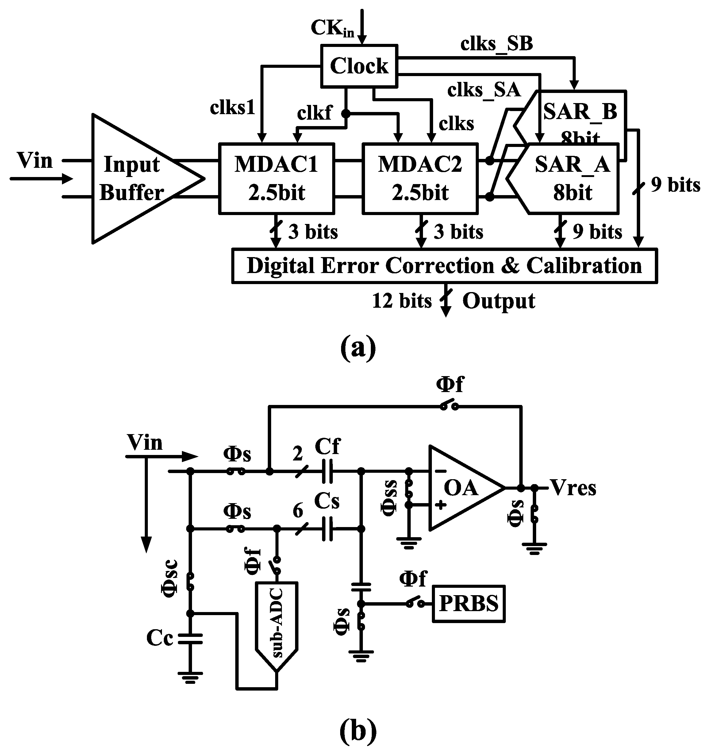
2. Proposed ADC Architecture

The block diagram of the proposed pipelined/SAR hybrid ADC is presented in Figure 1a. An input buffer is placed at the front-end to improve the ADC linearity in wideband and isolate the kick-back noise from the ADC sampling network, where the power consumption is essential to provide the low impedance especially for gigahertz sampling rate. The input signal is firstly digitized by two cascading MDACs. Each of them resolves 3 bits with 0.5bit-redundancy. And the TI-SAR quantizer resolves the last 8 bits with 9 bit cycles, where an extra cycle bit is added to alleviate the capacitive digital-to-analog converter (CDAC) and reference settling requirement. The flip-around topology is used for the MDACs to achieve higher feed-back factor as shown in Figure 1b. During the sampling phase, the input signal is sampled on the switch capacitors (Cs, Cf and Cc) by triggering Φ s s , Φ s and Φ s c in a specific order, where the signal dependent injection and the aperture error due to sample-and-hold-amplifier-less architecture can be prevented. As soon as the sampling phase finished, the sub-ADC makes its decision and propagates the results to the digital-to-analog-converter capacitors, which subtract the quantized analog voltage from the input signal. During the amplifying phase, a feedback loop is established by the operational amplifier (OA in Figure 1b) through triggering Φ f , passing the amplified residue signal to the next stage. Meanwhile the pseudorandom-bit-sequence circuit starts to work for assisting the capacitor mismatch and inter-stage gain calibration.
The timing diagram of the critical clock phases for each stage is shown in Figure 2. Early comparison scheme [24] is utilized to optimize the resolving time of sub-ADC and the settling time of operational amplifier. Out of the 1 ns dedicated for MDAC1, about 250 ps (clks1) are devoted to signal sampling, and the sub-ADC takes the next 250 ps to quantize the input. This leaves about 500 ps (clkf) for the operational amplifier to settle to the desired accuracy. As for the MDAC2, when the sampling time increases to about 500 ps (clkf), the quantization of sub-ADC takes place in the middle of the sampling phase, which results in a lower resolution of the signal sampled on the Cc compared to the Cs and Cf. Nevertheless the difference between the two sampling path can be equivalent to a comparator offset which can be corrected by the redundancy. During the amplifying phase (clks) of the MDAC2, the clks_SA and clks_SB are also enabled to track the residue signal of MDAC2 alternately. By implementing the asynchronous timing, several comparison cycles (B1~B9) are performed in series to complete one conversion for the last 8 bits within 1500 ps as shown in Figure 2.

3. Circuits Implementation and Calibration

3.1. Input Buffer

A source follower with cascode current source is used as the integrated input buffer as shown in Figure 3a, which determines the upper bound of the ADC linearity and achieves a wideband input frequency range. The large-signal transfer characteristic is derived as follows:
V i n V g s 0 = V o u t ,
If the gate-source voltage V g s 0 of the input transistor M0 is exactly constant, the output voltage V o u t follows the input voltage V i n with a constant difference. The distortion due to the input buffer is completely removed. With the square-law characteristic of a metal-oxide-semiconductor (MOS) transistor for qualitative analysis, the V g s 0 can be expressed as [25]:
V g s 0 = I d K × ( 1 + λ × V d s 0 ) + V t h 0 ,
where the V t h 0 is the threshold voltage of M0, V d s 0 is the drain-source voltage of M0 and I d is the current provided by the cascode current source. With λ = ( I d × rO0)−1 [25], Equation (2) can be rewritten as:
V g s 0 = I d K × ( I d + V d s 0 r O 0 ) + V t h 0 ,
where the rO0 is the output impedance of M0. The key point for the improvement of linearity is to suppress the variation of the items on the right side in Equation (3). First, the deep n-well layout is adopted to minimize the V t h 0 variation due to bulk effect. Second, the V d s 0 variation is inevitable because it is directly decided by V o u t . However a large rO0 can be obtained by setting the V o u t common-mode to as low as VDD/2, which reduces the effect of V d s 0 variation. Third, the Id variation is mainly contributed by the cascode current source which is affected by the V o u t as shown in Figure 3. For the nanometer CMOS technologies, the cascode current source is only moderately better than single transistor with a limited voltage headroom. A high voltage headroom can enhance the shielding ability of M1 to reduce the impact from V o u t , and alleviate the channel-length modulation for M2, which can eventually attenuate the Id variation. It can be seen that the high linearity requirement for input buffer has to be supported by a sufficiently high power supply.
The differential input buffer is optimized at different power supply via simulation. Figure 3b shows the fast Fourier transform (FFT) spectrum for Vout with a 101 MHz input signal at different power supply. With a power supply of 1.8 V, 76 dB spurious free dynamic range (SFDR) can be achieved. The linearity deteriorates as the power supply decreases. Especially M1 may enter the triode region when power supply drops to 1.2 V, where the Vds2 becomes sensitive to the Vout variation.

3.2. Operational Amplifier

A single-stage operational amplifier with telescopic cascode structure is employed for the residue amplifier in the MDACs to achieve wide bandwidth, good phase margin, and low noise as shown in Figure 4a. 1.8 V power supply is used to realize 1.2 Vpp signal swing, which can increase the voltage efficiency [23]. To optimize the bandwidth for 1 GS/s conversion rate, the operational amplifier is implemented with thin oxide devices, limiting the gain due to the low intrinsic device gain. The gain boosting technique is utilized to compensate the gain lose and achieve high linearity.
Usually a cascode amplifier serves as the gain-boosting stage (i.e., AP as shown in Figure 4a) in the high power supply as shown in Figure 4b [26]. However, when voltage efficiency is increased, it suffers from performance degradation. If 1.2 Vpp differential signal swing is realized with a common-mode of 0.9 V, the peak voltage of the single-side output of the operational amplifier would reach as high as 1.2 V as shown in Figure 4b. With 0.2 V allocated for the Vds of M1, the gate node of the input transistor M0 of AP has to be set to 1.4 V, which prevents M1 from entering the triode region with a full signal swing. Consequently, the Vgs of M0 is compressed to 0.4 V, where the M0 has to work in sub-threshold region. Moreover, this gain-boosting topology also brings in some difficulties in designing its gain-bandwidth product (GBW) for 1 GS/s conversion rate. It is well known that the gain-boosting stage would introduce a pair of pole-zero (doublet) into the amplifier transfer function which occurs near the GBW of the gain-boosting stage [27]. They produce the slow settling component, seriously degrading the settling behavior, when they are located in the low-frequency near the closed-loop dominant pole (Wd) as shown in Figure 4c [27]. As they are repelled to the high-frequency close to the 1st non-dominant pole (Wnd) in Figure 4c, the operational amplifier would become unstable [27]. There is a safe range between the Wd and Wnd to design the GBW for gain-boosting stage. It is noted that the Wnd is due to the cascode node (the AP input node) Vpi of the main amplifier as shown in Figure 4b. The Cgs is one of the capacitive load for Vpi, which is also the main parasitic capacitor of M0, and increases with the AP GBW. As a result, when increasing the AP GBW repels the doublet to the high-frequency, the Wnd is pulled to low frequency simultaneously due to the Cgs increased, compressing the safe range.
To address these issues, an improved gain-boosting stage (i.e., AP) is employed as shown in Figure 4d. A buffer is inserted between the main amplifier and the cascode amplifier, which decouples the signal swing and the input voltage of cascode amplifier, as well as the Wnd and AP GBW. A larger Vds for M1 can be set to enhance the main amplifier gain owing to the relaxed requirement for the AP input. And the capacitive load contributed by AP becomes the Cgb of M0’ that is much smaller than the Cgs. Thus, a relatively constant safe range can be maintained during adjusting the AP GBW.

3.3. Asynchronous SAR Quantizer

3.3.1. Architecture

Figure 5a shows the block diagram of the SAR quantizer for 8 least significant bits (LSBs) quantization. The higher conversion speed the single channel achieves, the less number of interleaved channels the TI-SAR quantizer requires. Both multi-bit/cycle conversion [4] and alternate comparators [28] for SAR quantizer can increase the conversion speed. However, the multi-bit/cycle conversion would reduce the advantages of redundancy and asynchronous timing [28] which are the main stream for SAR quantizer design. And its multiple CDACs increase the capacitive load heavily for the MDAC2, which results in a high power consumption. Therefore, an asynchronous clocking with alternate comparators [28] is employed to enhance the conversion speed of a single channel up to 500 MS/s, where 25% duty cycle is available for sampling phase.
The timing diagram of the SAR quantizer is presented in Figure 5b. The clks_SA/clks_SB are the clocks provided by the clock block referred to Figure 1a which define the sampling window and start the conversion. When the rising edge of clks_SA (or clks_SB) arrives, the CDAC starts to track the output of the MDAC2 through the sampling switch and the two comparators are in reset state. As the sampling phase is finished, the comparator CMP1 is triggered by CK1 to make the decision and the result is fed into the dynamic register. The end of CMP1 decision is sensed by the SAR logic and used to trigger CMP2 by activating CK2, then CMP1 is in reset state. This process repeats until all conversion step is completed. And the end of last conversion step activates the CKres which resets the CDAC to calibrate the comparator offset for one of the two comparators. Thus they can be calibrated alternately.

3.3.2. CDAC and Comparator

Figure 6 shows the CDAC array for splitting monotonic switching scheme [29] used by this SAR quantizer. To relax the settling time of the MSBs, the original 64-unit cells are split into 56-unit cells and 8-unit cells. And the 8-unit cells are inserted before the 4-unit cells as the redundant cycle. Then all even number of unit capacitors are split into two identical sub-capacitors. In the sampling phase, the bottom plate of half sub-capacitors are reset to Vref for each side, and the others are reset to ground as shown in Figure 6. At the same time, the input signal is sampled on the top-plate of the capacitors in the CDAC, where the first comparison can be performed immediately without switching capacitors, saving overall conversion time and 50% total capacitance. This is critical to achieve a low power consumption for the MDAC2. Next, when the conversion phase arrives, the comparators start to perform the comparison. According to the comparison results, the sub-capacitors on the higher voltage potential side are all connected to ground and the sub-capacitors on the other side are all connected to Vref. As the conversion proceeds to LSB, the switching method in Reference [6] is applied to the 1-unit cell. The resulting common-mode variation is negligible.
Besides the CDAC, the comparator is also the key block for the SAR quantizer which has the high influence on speed, determines the accuracy, and contributes significantly to the power consumption. A three-stage comparator used in this SAR quantizer is shown in Figure 7. A topology for high-speed, high-resolution comparator usually consists of a preamplifier and a regenerative latch. Both high gain and large bandwidth are required for the preamplifier to reduce the offset due to latch, as well as achieve the desired latch input voltage in minimum time. For the single amplifier, the gain-bandwidth product is assumed to be constant [30], which limits the capability. Therefore, the preamplifier is implemented by a two-stage cascaded dynamic amplifier (1st stage and 2nd stage) to reduce the input-referred offset with the propagation delay as small as possible. A Strong-ARM latch is usually adopted to achieve fast decision with the stacking of two cross-coupled pairs which require a large voltage headroom [31]. However, the thin-oxide devices in other blocks of SAR quantizer like high-speed CMOS switch are not adaptive to the high power supply due to the low break-down voltage. To simplify the power supply design, a topology with two cross-coupled pairs in parallel [31] is employed as the latch stage (3rd stage) in this comparator which requires just one threshold voltage plus two overdrive voltage to work in saturation as shown in Figure 7. The offset voltage cancellation of this comparator is implemented by a fast, low power self-calibrating technique [28]. A second differential pair Mcp and Mcn is introduced to compensate the offset as illustrated in Figure 7. The Mcp gate, Vcalp, is set to a constant voltage (usually the common-mode voltage) and a capacitor Ccal is attached to Vcaln. The calibration is performed as all conversion steps are completed and the CDAC is reset. According to the calibration result (outp_cal and outn_cal), charge is either added to the capacitor Ccal or subtracted from Ccal. Thus, the voltage Vcaln approaches the offset value of the comparator after several conversion period that is canceled in the conversion mode.

3.4. Adaptive Power/Ground

Because the SAR quantizer operating with 1 V power supply doesn’t comply with the 1.8 V input buffer and operational amplifier due to the difference of the common-mode voltage (0.5 V versus 0.9 V), the adaptive power/ground [23] is adopted to level-shift up the power and ground of the SAR quantizer, so that the common-mode voltage matches that of the input buffer and operational amplifier as shown in Figure 8. Moreover, the thin-oxide devices are also available for the CMOS switch in the MDACs with the adaptive power/ground.
The adaptive power/ground (VDDA and VSSA as shown in Figure 8) are generated using two low dropout regulators (LDOs). Besides supporting the implementation of thin-oxide devices, the VDDA and VSSA also provide the reference voltage to the CDACs of the TI-SAR quantizer, where the reference noise would significantly degrade the conversion accuracy. The use of on-chip decoupling capacitors is the most common noise suppression technique [32].
A hybrid structure for decoupling capacitor [32] is adopted to increase the capacitance density for saving the die area cost as shown in Figure 9a. The MOS decoupling capacitor is the most area-efficient and most commonly implemented structure owing to the dielectric layer provided by the gate oxide layer [32]. Therefore the hybrid structure is based on the thick oxide MOS which can minimize the leakage across the gate oxide layer. A multilayer metal decoupling capacitor is placed on the top of the thick oxide MOS decoupling capacitor, and they are connected to each other electrically in parallel. Thus a higher capacitance is achieved with the same die area. The layout of the hybrid structure for decoupling capacitor is illustrated in Figure 9a. In addition, this hybrid structure can also be used for the calibration capacitor Ccal in Figure 7, where a large capacitance of Ccal would enhance the calibration accuracy. Unfortunately, the MOS capacitance is reduced when applied in the low-voltage supply. With the adaptive power/ground, the operating voltage of the MOS capacitor can also be level-shifted up, avoiding to work in the weak inversion. And a high capacitance density can be achieved for Ccal as shown in Figure 9b.

3.5. Offset and Gain Calibration

The performance of interleaved channels is usually sensitive to the time skew, offset mismatches, and gain mismatches. Since the MDACs can serve as a track and hold circuit, the combined data from TI-SAR quantizer is free of images due to time skew. A calibration based on accumulation and average was proposed in Reference [21] to compensate the offset and gain mismatches as shown in Figure 10.
This calibration scheme includes an offset calibration loop and a gain calibration loop. The offset calibration loop uses an accumulator and average block to estimate and track the direct current value (DCV) of the channel output which is compared with that of the reference channel to generate an error signal ero. Next, the ero is applied to update the offset value which is subtracted from the raw output data. The similar process is executed by the gain calibration loop, where the mean absolute value (MAV) of the channel output is estimated and compared instead of the DCV. The implementation of this calibration is based on the assumption that the outputs of calibrated channel and reference channel should have the same DCV and MAV for the calibration signal in the ideal situation [21].
Nevertheless, when the calibration is applied for the TI-SAR quantizer in this hybrid ADC, the non-idealities of the MDACs would break the assumption above. Figure 11 illustrates the sampling points for the two interleaved channels (channel_cal and channel_ref) in the MDAC residue transfer curve with non-idealities. An asymmetry of the MDAC residue transfer curve is caused by the non-idealities, which changes the statistical characteristics of the two groups of sampling points, as well as results in an offset between their DCVs as shown in Figure 11. And it is similar to the MAVs.
The effect of the non-idealities is demonstrated in a behavioral simulation. A behavioral model of the ADC shown in Figure 1a has been implemented in software. The typical non-idealities such as comparator offset and capacitor mismatches are taken into account for the MDACs. And the SAR quantizer is modeled as an ideal converter. In this simulation, a sine wave is sampled by the ADC. And the residue output of the MDAC2 is also used as the calibration signal for the TI-SAR quantizer, of which the digital outputs are collected to calculate the DCVs and MAVs.
The differences of the DCVs and MAVs for the TI-SAR outputs are shown in Figure 12. For the ideal MDACs (without non-idealities), the differences of the DCVs and MAVs converge quickly to zero as the number of points collected increases, which fulfills the statistical requirements for the offset and gain calibration. However, when the non-idealities of the MDACs are taken into account (with non-idealities), a fixed offset are introduced between the DCVs for the TI-SAR outputs, and so do the MAVs. Thus, these offsets would be mistaken for the interchannel mismatches by the calibration algorithm in Figure 10, degrading the calibration performance.
To improve the calibration performance, a calibration scheme based on the VIC is developed as shown in Figure 13. First, the capacitor mismatch and inter-stage gain error are corrected with the calibration technique in Reference [33]. And the comparator offset is tolerated by the MDAC redundancy (digital error correction). Second, the encoded data is divided into even and odd sequences which are regarded as the VIC outputs. The offset and gain mismatches of the TI-SAR quantizer can be transformed to that of the VIC, because the TI-SAR outputs are included in each sequence respectively. Third, the offset and gain calibration in Figure 10 is performed with the two sequences as the input.
There are two benefits of this calibration scheme. First, the non-idealities cancellation not only improves the ADC performance but also minimizes the detrimental effects for the subsequent offset and gain calibration. Second, the calibration signal for the VIC is usually an alternating current signal which fulfills the statistical requirements for the offset and gain calibration.
Figure 14 shows the differences of the DCVs and MAVs for the TI-SAR outputs, as well as the VIC outputs, when the non-idealities of front MDACs are taking into account. Compared with the TI-SAR outputs, the difference of DCVs and MAVs for the VIC outputs converges quickly to zero, which is more suitable for the offset and gain calibration.

4. Measured Results and Discussion

The 1 GS/s 12-bit pipelined/SAR hybrid ADC is fabricated in a 40 nm CMOS technology. Figure 15 presents the die microphotograph. It occupies an active area of 0.47 mm × 0.25 mm. The static performance of the differential nonlinearity (DNL) and integral nonlinearity (INL) is presented in Figure 16. The measured DNL and INL are −0.94/+0.85 LSB and −3.4/+3.9 LSB, respectively.
Figure 17 depicts the measured FFT of the ADC output. The signal-to-noise-and-distortion ratio (SNDR) and SFDR achieve 58.2 dB and 72 dB respectively at 69 MHz input frequency as shown in Figure 17a. When the input frequency increases to 1814 MHz in the fourth Nyquist zone, the SNDR and SFDR can maintain 55.3 dB and 64 dB as shown in Figure 17b, which is contributed by the integrated input buffer. For the ADC with external input buffer, the fluctuation of sampled signal due to the parasitic inductance in the bonding wire requires more time to eliminate for achieving high linearity, which limits the sampling rate seriously. And the asymmetric signal path of the bonding wire also induces the even harmonic distortion in the high-frequency input. Although the TI-SAR in this hybrid architecture can avoid the time skew error, the bandwidth mismatch also may limit the SFDR performance as shown in Figure 17b.
The offset and gain calibrations based on both TI-SAR outputs and VIC outputs are implemented. The SNDR and SFDR performance versus the input frequency is shown in Figure 18. Both calibrations can improve the SNDR and SFDR. Nevertheless, the calibration performance based on TI-SAR outputs is attenuated compared with that based on VIC outputs due to the statistical deviation of the TI-SAR input signal.
The core ADC consumes 94 mW, including the 24 mW dissipated by the input buffer. The F O M achieves 0.14 pJ/step according to the formula:
F O M = P o w e r 2 ( S N D R 1.76 6.02 ) × f s .
Table 1 compares the measurement results with the state-of-art ADCs. For the gigahertz sampling rate and high resolution ADCs, a simple TI-SAR architecture is difficult to achieve a good FOM due to the reasons discussed in Section 1, which means it would trade larger power consumption for performance. And the multi-MDACs bring about some difficulties in further improvement for the pipeline architecture. The work in this paper combines the advantages of both ADC topologies to achieve a low FOM and alleviates the stringent headroom requirements of precision analog circuit design in advanced CMOS technologies.

5. Conclusions

In this paper, a 1 GS/s 12-bit pipelined/SAR hybrid ADC is implemented in a 40 nm CMOS technology for various applications. An input buffer is integrated on-chip to achieve high linearity at 1.8 V which also extends the input frequency to the fourth Nyquist zone. With the same power supply, a single-stage operational amplifier with telescopic cascode structure is used to achieve 1.2 Vpp signal swing stably at 1 GS/s conversion rate which increases the voltage efficiency with an improved gain-boosting stage. And a 500 MS/s 8-bit SAR quantizer with alternate comparators at 1 V is designed to minimize the number of the required interleaved channels, simplifying the complexity. To achieve the compatibility between the blocks in different power supply, an adaptive power/ground is used to compensate their common-mode mismatch and avoid the negative supply. Although the time skew error of TI-SAR quantizer, the most critical challenge for time-interleaved channels, is removed by the hybrid architecture, the remaining offset and gain mismatches still degrade the ADC performance. Nevertheless, the traditional calibration performance for theses mismatches would deteriorate in this hybrid architecture due to the non-idealities of the front MDACs. A calibration scheme based on the VIC is developed to calibrate the offset and gain mismatches, which realizes the improvement on both SNDR and SFDR.

Author Contributions

J.L. (Jianwen Li) designed the circuits, analyzed the measurement data, and wrote the manuscript. X.G., J.L. (Jian Luan), D.W. and L.Z. assisted the circuits implementation and simulation. N.W. wrote the test program for this chip. Y.H. assisted the chip package implementation and the PCB designing. H.J. performed the chip test. X.Z. and J.W. contributed to the technical discussions and reviewed the manuscript. X.L. gave some valuable guidance and confirmed the final version of manuscript. All authors have read and agreed to the published version of the manuscript.

Funding

This research was funded by the National Key Research and Development Program of China (Grant No. 2018YFB2202302).

Conflicts of Interest

The authors declare no conflict of interest.

Abbreviations

The following abbreviations are used in this manuscript:
ADCanalog-to-digital converter
CMOScomplementary metal-oxide-semiconductor
SARsuccessive-approximation-register
TI-SARtime-interleaved SAR
MDACmultiplying digital-to-analog converter
MSBmost significant bit
Vpppeak-to-peak voltage
LSBleast significant bit
FOMfigure of merit
MOSmetal-oxide-semiconductor
VICvirtually-interleaved channels
CDACcapacitive digital-to-analog converter
FFTfast Fourier transform
GBWgain-bandwidth product
LDOlow dropout regulator
DCVdirect current value
MAVmean absolute value
DNLdifferential nonlinearity
INLintegral nonlinearity
SNDRsignal-to-noise-and-distortion ratio
SFDRspurious free dynamic range

References

  1. Le Dortz, N.; Blanc, J.; Simon, T.; Verhaeren, S.; Rouat, E.; Urard, P.; Le Tual, S.; Goguet, D.; Lelandais-Perrault, C.; Benabes, P. A 1.62GS/s time-interleaved SAR ADC with digital background mismatch calibration achieving interleaving spurs below 70dBFS. In Proceedings of the 2014 IEEE International Solid-State Circuits Conference, San Francisco, CA, USA, 9–13 February 2014; pp. 386–388. [Google Scholar]
  2. Zhu, Y.; Chan, C.; Seng-Pan, U.; Martins, R.P. An 11b 900 MS/s time-interleaved sub-ranging pipelined-SAR ADC. In Proceedings of the 2014—40th European Solid State Circuits Conference, Venice Lido, Italy, 22–26 September 2014; pp. 211–214. [Google Scholar]
  3. Louwsma, S.M.; van Tuijl, A.J.M.; Vertregt, M.; Nauta, B. A 1.35 GS/s, 10 b, 175 mW Time-Interleaved AD Converter in 0.13 μm CMOS. IEEE J. Solid-State Circuit 2008, 43, 778–786. [Google Scholar] [CrossRef]
  4. Wei, H.; Chan, C.; Chio, U.; Sin, S.; Seng-Pan, U.; Martins, R.P.; Maloberti, F. An 8-b 400-MS/s 2-b-Per-Cycle SAR ADC with Resistive DAC. IEEE J. Solid-State Circuit 2012, 47, 2763–2772. [Google Scholar]
  5. Zhu, Y.; Chan, C.; Sin, S.; Seng-Pan, U.; Martins, R.P.; Maloberti, F. A 50-fJ 10-b 160-MS/s Pipelined-SAR ADC Decoupled Flip-Around MDAC and Self-Embedded Offset Cancellation. IEEE J. Solid-State Circuit 2012, 47, 2614–2626. [Google Scholar] [CrossRef]
  6. Liu, C.; Chang, S.; Huang, G.; Lin, Y. A 10-bit 50-MS/s SAR ADC with a Monotonic Capacitor Switching Procedure. IEEE J. Solid-State Circuit 2010, 45, 731–740. [Google Scholar] [CrossRef]
  7. Liu, W.; Huang, P.; Chiu, Y. A 12-bit, 45-MS/s, 3-mW Redundant Successive-Approximation-Register Analog-to-Digital Converter with Digital Calibration. IEEE J. Solid-State Circuit 2011, 46, 2661–2672. [Google Scholar] [CrossRef]
  8. Zhou, Y.; Xu, B.; Chiu, Y. A 12 bit 160 MS/s Two-Step SAR ADC with Background Bit-Weight Calibration Using a Time-Domain Proximity Detector. IEEE J. Solid-State Circuit 2015, 50, 920–931. [Google Scholar] [CrossRef]
  9. Jae-Won, N.; Hassanpourghadi, M.; Aoyang, Z.; Mike Shuo-Wei, C. A 12-bit 1.6 GS/s interleaved SAR ADC with dual reference shifting and interpolation achieving 17.8 fJ/conv-step in 65nm CMOS. In Proceedings of the 2016 IEEE Symposium on VLSI Circuits, Honolulu, HI, USA, 15–17 June 2016; pp. 1–2. [Google Scholar]
  10. Nam, J.; Hassanpourghadi, M.; Zhang, A.; Chen, M.S. A 12-Bit 1.6, 3.2, and 6.4 GS/s 4-b/Cycle Time-Interleaved SAR ADC With Dual Reference Shifting and Interpolation. IEEE J. Solid-State Circuit 2018, 53, 1765–1779. [Google Scholar] [CrossRef]
  11. Doris, K.; Janssen, E.; Nani, C.; Zanikopoulos, A.; Weide, G.V.D. A 480 mW 2.6 GS/s 10b Time-Interleaved ADC with 48.5 dB SNDR up to Nyquist in 65 nm CMOS. IEEE J. Solid-State Circuit 2011, 46, 2821–2833. [Google Scholar] [CrossRef]
  12. Janssen, E.; Doris, K.; Zanikopoulos, A.; Murroni, A.; Weide, G.V.D.; Lin, Y.; Alvado, L.; Darthenay, F.; Fregeais, Y. An 11b 3.6GS/s time-interleaved SAR ADC in 65nm CMOS. In Proceedings of the 2013 IEEE International Solid-State Circuits Conference, San Francisco, CA, USA, 17–21 February 2013; pp. 464–465. [Google Scholar]
  13. Young-Deuk, J.; Young-Kyun, C.; Jae-Won, N.; Kwi-Dong, K.; Woo-Yol, L.; Kuk-Tae, H.; Jong-Kee, K. A 9.15 mW 0.22 mm2 10b 204 MS/s pipelined SAR ADC in 65nm CMOS. In Proceedings of the IEEE Custom Integrated Circuits Conference, San Jose, CA, USA, 19–22 September 2010; pp. 1–4. [Google Scholar]
  14. Zhong, J.; Zhu, Y.; Sin, S.; Seng-Pan, U.; Martins, R.P. Thermal and Reference Noise Analysis of Time-Interleaving SAR and Partial-Interleaving Pipelined-SAR ADCs. IEEE Trans. Circuits Syst. I-Regul. Pap. 2015, 62, 2196–2206. [Google Scholar] [CrossRef]
  15. Ali, A.M.A.; Dinc, H.; Bhoraskar, P.; Dillon, C.; Puckett, S.; Gray, B.; Speir, C.; Lanford, J.; Brunsilius, J.; Derounian, P.R.; et al. A 14 Bit 1 GS/s RF Sampling Pipelined ADC with Background Calibration. IEEE J. Solid-State Circuit 2014, 49, 2857–2867. [Google Scholar] [CrossRef]
  16. Hershberg, B.; Dermit, D.; Liempd, B.V.; Martens, E.; Markulic, N.; Lagos, J.; Craninckx, J. A 3.2GS/s 10 ENOB 61mW Ringamp ADC in 16nm with Background Monitoring of Distortion. In Proceedings of the 2019 IEEE International Solid- State Circuits Conference, San Francisco, CA, USA, 17–21 February 2019; pp. 58–60. [Google Scholar]
  17. Lagos, J.; Hershberg, B.P.; Martens, E.; Wambacq, P.; Craninckx, J. A 1-GS/s, 12-b, Single-Channel Pipelined ADC with Dead-Zone-Degenerated Ring Amplifiers. IEEE J. Solid-State Circuit 2019, 54, 646–658. [Google Scholar] [CrossRef]
  18. Dongsheng, M.; Wing-Hung, K.; Chi-Ying, T. An integrated one-cycle control buck converter with adaptive output and dual loops for output error correction. IEEE J. Solid-State Circuit 2004, 39, 140–149. [Google Scholar]
  19. Huang, H.; Xu, H.; Elies, B.; Chiu, Y. A Non-Interleaved 12-b 330-MS/s Pipelined-SAR ADC with PVT-Stabilized Dynamic Amplifier Achieving Sub-1-dB SNDR Variation. IEEE J. Solid-State Circuit 2017, 52, 3235–3247. [Google Scholar] [CrossRef]
  20. Lim, Y.; Flynn, M.P. A 100 MS/s, 10.5 Bit, 2.46 mW Comparator-Less Pipeline ADC Using Self-Biased Ring Amplifiers. IEEE J. Solid-State Circuit 2015, 50, 2331–2341. [Google Scholar] [CrossRef]
  21. Hsu, C.; Huang, F.; Shih, C.; Huang, C.; Lin, Y.; Lee, C.; Razavi, B. An 11b 800 MS/s Time-Interleaved ADC with Digital Background Calibration. In Proceedings of the 2007 IEEE International Solid-State Circuits Conference, San Francisco, CA, USA, 11–15 February 2007; pp. 464–615. [Google Scholar]
  22. Guerber, J.; Gande, M.; Moon, U. The Analysis and Application of Redundant Multistage ADC Resolution Improvements Through PDF Residue Shaping. IEEE Trans. Circuits Syst. I-Regul. Pap. 2012, 59, 1733–1742. [Google Scholar] [CrossRef] [Green Version]
  23. Chen, C.; Wu, J.; Hung, J.; Li, T.; Liu, W.; Shih, W. A 12-Bit 3 GS/s Pipeline ADC With 0.4 mm2 and 500 mW in 40 nm Digital CMOS. IEEE J. Solid-State Circuit 2012, 47, 1013–1021. [Google Scholar] [CrossRef]
  24. Byung-Moo, M.; Kim, P.; Bowman, F.W.; Boisvert, D.M.; Aude, A.J. A 69-mW 10-bit 80-MSample/s Pipelined CMOS ADC. IEEE J. Solid-State Circuit 2003, 38, 2031–2039. [Google Scholar] [CrossRef]
  25. Razavi, B. Basic MOS Device Physics. In Design of Analog CMOS Integrated Circuits, 2nd ed.; McGraw-Hill Education: New York, NY, USA, 2017; pp. 7–44. [Google Scholar]
  26. Gentinne, B.; Colinge, J.P.; Jespers, P.G.A.; Eggermont, J.P. Improvement of the performances of SOI CMOS operational amplifiers by means of a gain-boosting stage. In Proceedings of the 1993 IEEE International SOI Conference, Palm Springs, CA, USA, 5–7 October 1993; pp. 184–185. [Google Scholar]
  27. Bult, K.; Geelen, G.J.G.M. A fast-settling CMOS op amp for SC circuits with 90-dB DC gain. IEEE J. Solid-State Circuit 1990, 25, 1379–1384. [Google Scholar] [CrossRef]
  28. Kull, L.; Toifl, T.; Schmatz, M.; Francese, P.A.; Menolfi, C.; Brändli, M.; Kossel, M.; Morf, T.; Andersen, T.M.; Leblebici, Y. A 3.1 mW 8b 1.2 GS/s Single-Channel Asynchronous SAR ADC with Alternate Comparators for Enhanced Speed in 32 nm Digital SOI CMOS. IEEE J. Solid-State Circuit 2013, 48, 3049–3058. [Google Scholar] [CrossRef]
  29. Liu, C.; Chang, S.; Huang, G.; Lin, Y.; Huang, C. A 1V 11fJ/conversion-step 10bit 10 MS/s asynchronous SAR ADC in 0.18 μm CMOS. In Proceedings of the 2010 Symposium on VLSI Circuits, Honolulu, HI, USA, 16–18 June 2010; pp. 241–242. [Google Scholar]
  30. Allen, P.E.; Holberg, D.R. Comparators. In CMOS Analog Circuit Design, 3rd ed.; Oxford University Press, Inc.: New York, NY, USA, 2012; pp. 444–497. [Google Scholar]
  31. Kuo, B.; Chen, B.; Tsai, C. A 0.6V, 1.3GHz dynamic comparator with cross-coupled latches. In Proceedings of the VLSI Design, Automation and Test, Hsinchu, Taiwan, 27–29 April 2015; pp. 1–4. [Google Scholar]
  32. Charania, T.; Opal, A.; Sachdev, M. Analysis and Design of On-Chip Decoupling Capacitors. IEEE Trans. Very Large Scale Integr. (VLSI) Syst. 2013, 21, 648–658. [Google Scholar] [CrossRef]
  33. Zheng, X.; Wang, Z.; Li, F.; Zhao, F.; Yue, S.; Zhang, C.; Wang, Z. A 14-bit 250 MS/s IF Sampling Pipelined ADC in 180 nm CMOS Process. IEEE Trans. Circuits Syst. I-Regul. Pap. 2016, 63, 1381–1392. [Google Scholar] [CrossRef] [Green Version]
  34. Vecchi, D.; Mulder, J.; van der Goes, F.M.L.; Westra, J.R.; Ayranci, E.; Ward, C.M.; Wan, J.; Bult, K. An 800 MS/s Dual-Residue Pipeline ADC in 40 nm CMOS. IEEE J. Solid-State Circuit 2011, 46, 2834–2844. [Google Scholar] [CrossRef]
  35. Wu, J.; Chen, C.; Li, T.; He, L.; Liu, W.; Shih, W.; Tsai, S.S.; Chen, B.; Huang, C.; Hung, B.J.; et al. A 240-mW 2.1-GS/s 52-dB SNDR Pipeline ADC Using MDAC Equalization. IEEE J. Solid-State Circuit 2013, 48, 1818–1828. [Google Scholar]
Figure 1. (a) Proposed pipelined/successive-approximation-register (pipelined/SAR) hybrid analog-to-digital converter (ADC). (b) Block diagram of the flip-around multiplying digital-to-analog converter (MDAC) used in this hybrid ADC. The PRBS is used to assist the capacitor mismatch and inter-stage gain calibration.
Electronics 09 00375 g001
Figure 2. Timing diagram of the critical clock phases for each stage. Asynchronous clocking is used for the SAR quantizer.
Electronics 09 00375 g002
Figure 3. (a) Schematic of the input buffer. A topology of source follower with cascode current source is adopted for the input buffer. (b) Simulated fast Fourier transform (FFT) spectrum of the input buffer output with a 101 MHz input signal in different power supply.
Electronics 09 00375 g003
Figure 4. (a) Schematic of the operational amplifier in MDACs. Four gain-boosting stages (APs and ANs) are utilized to compensate the gain loss due to low intrinsic device gain. (b) Illustration of the cascode amplifier as gain-boosting stage. (c) Pole zero locations for the operational amplifier with the gain-boosting stage in (b). (d) Illustration of the improved gain-boosting stage. A buffer is inserted between the main amplifier and the cascode amplifier.
Electronics 09 00375 g004
Figure 5. Scheme of the SAR quantizer. (a) Block diagram of the architecture with alternate comparators and (b) timing diagram. It can achieve a conversion speed of up to 500 MS/s with 25% duty cycle for sampling phase.
Electronics 09 00375 g005
Figure 6. The capacitive digital-to-analog converter (CDAC) array for splitting monotonic switching scheme. Top-plate sampling can save one cycle bit and 50% total capacitance.
Electronics 09 00375 g006
Figure 7. Circuit implementation of the comparator in the SAR quantizer. A topology of three-stage comparator is implemented to achieve high-speed and high-resolution.
Electronics 09 00375 g007
Figure 8. Illustration of the adaptive power/ground. It compensates the common-mode voltage mismatch and enables the application of thin-oxide device in high-speed blocks.
Electronics 09 00375 g008
Figure 9. (a) Hybrid structure of the capacitor for decoupling and calibration. (b) Illustration of the capacitor level-shifting by the adaptive power/ground. The application of capacitors with hybrid structure increases the capacitance density to save the total die area.
Electronics 09 00375 g009
Figure 10. Conventional calibration scheme for the offset and gain mismatches. Statistical requirements have to be fulfilled while implementing this calibration scheme.
Electronics 09 00375 g010
Figure 11. Illustration of the sampling points for the two interleaved channels in the MDAC residue transfer curve with a sine waveform as input. The two groups of sampling points have different statistical characteristics.
Electronics 09 00375 g011
Figure 12. Differences of the (a) direct current values (DCVs) and (b) mean absolute values (MAVs) for the time interleaved-SAR (TI-SAR) outputs with and without the non-idealities of front MDACs.
Electronics 09 00375 g012
Figure 13. Developed calibration scheme based on the virtually-interleaved channels (VIC). The non-idealities cancelation, as well as offset and gain calibration, are both included in this calibration scheme. And the VIC outputs can fulfill the statistical requirements for calibration algorithm in Figure 10.
Electronics 09 00375 g013
Figure 14. Differences of the (a) DCVs and (b) MAVs for the TI-SAR outputs, as well as the VIC outputs, taking the non-idealities of front MDACs into account.
Electronics 09 00375 g014
Figure 15. Die microphotograph. The size of core ADC is 0.47 mm × 0.25 mm.
Electronics 09 00375 g015
Figure 16. Measured differential nonlinearity (DNL) and integral nonlinearity (INL) of this hybrid ADC. There is no missing code.
Electronics 09 00375 g016
Figure 17. Measured FFT spectrum at 1 GS/s for the input frequency of (a) 69 MHz and (b) 1814 MHz.
Electronics 09 00375 g017
Figure 18. Measured spurious free dynamic range (SFDR) and signal-to-noise-and-distortion ratio (SNDR) versus input frequency at 1 GS/s.
Electronics 09 00375 g018
Table 1. Summarization of the performance for this work and comparison with state-of-art ADCs.
Reference[11][12][34][35]This Work
ArchitectureTI-SARTI-SARTI-PipelineTI-PipelinePipelined/SAR
TechnologyCMOS 65 nmCMOS 65 nmCMOS 40 nmCMOS 40 nmCMOS 40 nm
Sampling rate (GS/s)2.63.60.82.11
Resolution (bits)1011121212
Supply (V)1.2/1.3/1.61.2/2.51/2.52.51.8
SNDR@Nyquist (dB)48.542595258
SFDR@Nyquist (dB)53.850706268
Power (mW)48079510524094
FOM@Nyquist (pJ/step)0.852.150.180.430.14

