Article

Comparative Evaluation of Wide-Range Soft-Switching PWM Full-Bridge Modular Multilevel DC–DC Converters

School of Electrical and Control Engineering, Shaanxi University of Science and Technology, Xi’an 710021, China
*
Author to whom correspondence should be addressed.
Electronics 2020, 9(2), 231; https://doi.org/10.3390/electronics9020231
Submission received: 26 December 2019 / Revised: 26 January 2020 / Accepted: 27 January 2020 / Published: 31 January 2020
(This article belongs to the Special Issue Power Converters in Power Electronics)

Abstract

:
This paper discusses some wide-range soft-switching full-bridge (FB) modular multilevel dc–dc converters (MMDCs), and a comparative evaluation of these FB MMDCs is also presented. The discussed topologies have all merits belonging to conventional FB MMDCs, e.g., smaller voltage stress on the primary switches, no added primary clamping devices and modular primary structure. In addition, the primary switches in each converter can obtain zero-voltage switching (ZVS) or zero-current switching (ZCS) in a wide load range. Two presented topologies are selected as examples to discuss in detail. The proposed FB MMDCs are assessed and evaluated based on performance, components and topology structure indices, such as soft switching characteristics, current stress, power loss distribution, number of added devices, complexity of structure and added cost. Experimental results are also included to verify the feasibility and advantages of the new topologies.

1. Introduction

With the rapid development of smart grid systems, dc-based distributed power systems and micro grids attract more and more attention due to some clearly good features, e.g., high power transfer efficiency, low system cost, high system stability and easy system control [1,2]. Commonly, the input voltage of these dc interfaces is very high to obtain optimum system performance, which makes high input voltage and high frequency isolated dc-dc converters become hot and causes challenging issues in power electronics. In the high voltage applications, how to reduce the voltage stress on the primary switches is a key point, and several methods can be used to solve this problem. The first way is to connect the power switches in series directly, but this method is seldom used in the high frequency applications due to the serious static and dynamic voltage balance problems [3]. Second, three-level (TL) dc-dc converters (TLDCs) are suitable topologies for high voltage applications due to only half the input voltage stress on the primary switches [4]. The first diode-clamped TLDC was proposed in 1992 [4], and then, many other efforts have been made on this topic, e.g., novel topologies and corresponding control strategies [4,5,6,7,8,9,10,11], wide range soft switching solutions [12,13,14,15,16] and reduced filter size solutions [16,17,18,19]. Finally, modular multilevel dc-dc converters (MMDCs) can also be used in high voltage applications [20]. MMDCs are built of modular cells with input series and output series or parallel connected, and can be extended to higher voltage levels easily due to their modular structure. Many TLDCs, e.g., diode-clamped TLDCs, can also be extended to a higher voltage level. But, as mentioned in [20], the number of achievable voltage levels is limited due to not only the dynamic voltage unbalance problem but also the complexity of the primary circuit structure and modulation strategy. Therefore, MMDCs may be a better choice for applications with super high input voltage, i.e., 1400 V or higher. A half bridge (HB) MMDC was proposed and discussed in [4], which is built of two-level HB modules. Several HB MMDCs for higher input voltage ratings have been proposed [21,22]. In [23], an FB MMDC was proposed, which is composed of two input series and output series connected two-level FB cells. Compared to HB MMDCs, FB MMDCs are more suitable for high input and large power industry applications due to the lower VA rating of the primary components, more modular structure and easy control. A number of new FB MMDCs were proposed and discussed in [20,23,24,25,26]. A new FB MMDC with auto-balance ability among series connected primary modules was proposed in [20]. Controlling strategies for output parallel-connected FB MMDCs were analyzed in [27,28,29]. However, improvements are still required. In the high voltage applications, soft switching performance of the primary switches is a key point to ensure higher efficiency due to the switching loss increases squared with the input voltage. Fortunately, the switching scheme of FB MMDCs is quite similar to that of the two-level phase shift (PS) FB dc-dc converter. Hence, common wide-range soft-switching solutions for conventional two-level PS FB dc-dc converters can be directly used in FB MMDCs. But, the system performance, structure complexity and added cost of different solutions for FB MMDCs are quite different because more primary cells are involved. Therefore, wide-range soft-switching FB MMDCs and a comparative evaluation of these solutions are still interesting subjects.
In this paper, some new wide-range soft-switching FB MMDCs are discussed and compared.
The main contributions of this paper are:
(1)
Based on conventional FB MMDC, this paper proposes eight novel soft-switching solutions;
(2)
Through comparative study of them, the two most promising switching solutions are found;
(3)
Converter losses, efficiency and costs of the two solutions are analyzed and tested for verification.
This paper is organized as follows. In Section 2, the circuits of the presented converters are described. The operation principles and relevant analysis of an improved zero-voltage switching (IZVS) FB MMDC are provided in Section 3. The operation principles and relevant analysis of a zero-voltage and zero-current switching (ZVZCS) FB MMDC are discussed in Section 4. A comparative evaluation of the presented converters is provided in Section 5. In Section 6, experimental results are presented and analyzed. Finally, some brief conclusions are given.

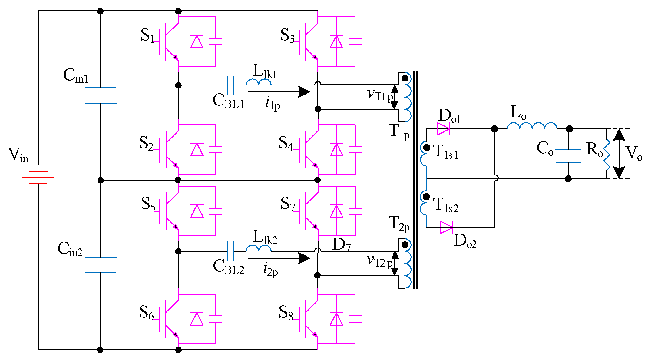
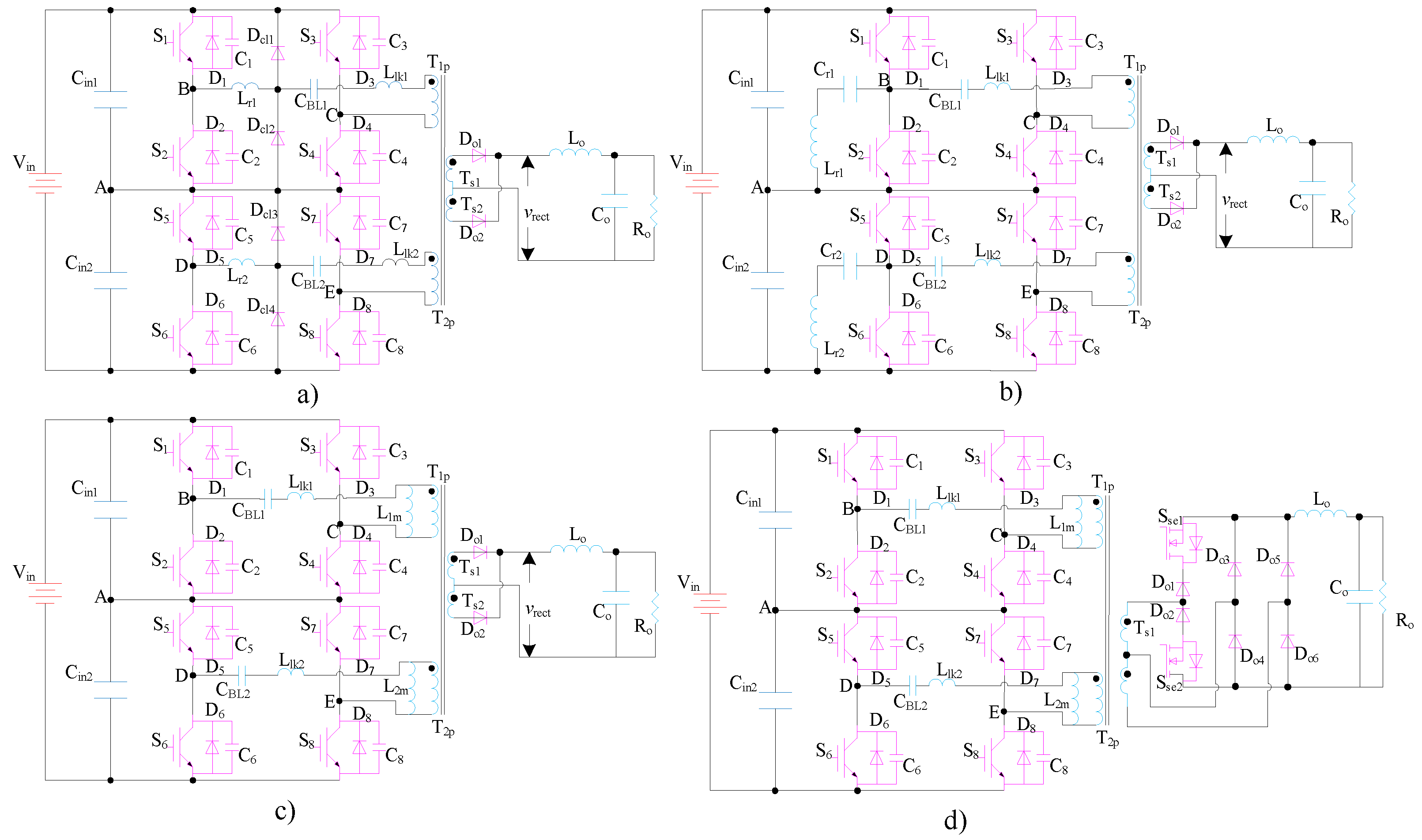
2. Wide-Range Soft-Switching PWM FB MMDCs

Figure 1 illustrates a conventional FB MMDC, which is built of two two-level FB cells. The switches in each cell are switched in PS mode. Thus, eight switches in Figure 1 can also be divided into two groups, i.e., the leading and lagging switches. The lagging switches will face more difficulty to obtain ZVS because only the energy stored in the leakage inductances can be used.
As the switching scheme of Figure 1 is quite similar to that of a two-level PS FB dc-dc converter, common wide-range soft-switching solutions for two-level PS FB dc-dc converters can also be used [30,31,32,33,34,35,36,37]. These solutions can be concluded into two types: IZVS and ZVZCS. IZVS converters extend the ZVS range of the lagging switches by increasing either the value of the primary equivalent inductance or the currents of the switches [30,31,32,33,34]. In the ZVZCS converters, the lagging switches can realize ZCS by resetting the primary current during the free-wheeling mode. According to the different reset voltage generated methods, the ZVZCS converters can be further divided into two kinds, which are primary reset and secondary reset ZVZCS converters [35,36,37]. Generally, ZVZCS solutions are more suitable for the converters with IGBTs because of the large tailing current during the switching commutation.

2.1. IZVS FB MMDCs

Figure 2 shows four IZVS FB MMDCs. In IZVS_CD, the upper FB primary cell is built of the switches S1 to S4, the primary coil T1p, Lr1, Dcl1, Dcl2 and the blocking capacitor CBL1; another primary cell is comprised of the switches S5 to S8, the primary coil T2p, Lr2, Dcl3, Dcl4 and the blocking capacitor CBL2. Lr1 and Lr2 are added to enlarge ZVS range of the lagging switches. Dcl1 to Dcl4 are used to eliminate the oscillation and clamp the secondary rectified voltage reflected to the primary side. The power transformer is built of two independent magnetic cores, two primary coils and two common secondary coils. Each primary coil is wired around an independent magnetic core; while the common secondary coils enclose both cores. Cin1 and Cin2 are the input capacitors with the same value, and these capacitors share the input voltage evenly during the operation stages, i.e., V Cin 1 = V Cin 2 = V in / 2 . Llk1 and Llk2 are leakage inductances of T1p and T2p. Do1 and Do2 are the rectifier diodes, and the output filter is built of Lo and Co. Ro is the load resistor.
In IZVS_CAC, two commutation auxiliary circuits (CACs) are added to enlarge the ZVS range of the lagging switches. The secondary rectifier of IZVS_CAC is identical to that of IZVS_CD. The configuration of IZVS_SMI is quite similar to that of Figure 1. However, the magnetic currents of the transformer in IZVS_SMI are increased to provide more resonant energy. The structure of the power transformers in IZVS_CAC and IZVS_SMI is identical to that of IZVS_CD. IZVS_SMM shows a secondary modulated FB MMDC. The primary structure of IZVS_SMM is identical to that of IZVS_SMI, and the magnetizing currents are also increased to help the ZVS of the primary switches. The transformer in IZVS_SMM has two primary coils and two secondary coils. Do3 to Do6 are the rectifier diodes. Sse1 and Sse2 are two added secondary switches. The output filter is built of Lo and Co. Ro is the load resistor.

2.2. ZVZCS FB MMDCs

Figure 3 depicts four ZVZCS FB MMDCs. IZVZCS_DCF is a primary current reset ZVZCS converter with two cut-off diodes in each FB cell. CBL1 and CBL2 are designed to a specific value to reset the primary currents. D3, D4, D7 and D8 are used to block the reverse primary currents. The secondary circuit of IZVZCS_DCF equals that of IZVS_CD. IZVZCS_SAC&CAC and IZVZCS_SRC&CAC illustrate two secondary reset ZVZCS FB MMDCs. In IZVZCS_SAC&CAC, Sse and Cse are added to conventional FB MMDC to reset the primary currents; while the secondary reset circuit in IZVZCS_SRC&CAC has the same function, which is composed of Dse1, Dse2 and Cse. In IZVZCS_SI, CBL1 and CBL2 are designed to a specific value to reset the primary currents, and two saturable inductors, i.e., Lr1 and Lr2, are used to limit the reverse primary currents. The structure of the power transformers in Figure 3 is identical to that of IZVS_CD.

3. IZVS FB MMDC with Secondary Modulated

In order to simplify the description, the operation principle and characteristics of IZVS_CD, IZVS_CAC and IZVS_SMI is not presented here, and corresponding information can be found in [30,31,32,33]. The IZVS_SMM is selected as an example to analyze in detail in this part.

3.1. Operation Principle

Key waveforms of IZVS_SMM are shown in Figure 4. There are six operation stages during the whole switching cycle, and the operation stages in the first half switching cycle are illustrated in Figure 5. Before the analysis, some assumptions are set to simplify the explanation: all the components in the topology are ideal; Cin1 and Cin2 are large enough to be considered as voltage sources valued V in / 2 , and the voltage ripple on them can be neglected; CBL1 and CBL2 are large enough, and the voltage ripple on them can be neglected; L m 1 = L m 2 = L m ; L L 1 K 1 = L L 1 K 2 = L 1 K ; Im is the peak value of the magnetizing currents; output filter and load are replaced by a constant current source Io; kT1 and kT2 are the turn ratios k T = ( k T 1 × k T 2 ) / ( k T 1 + k T 2 ) . The output capacitance of each switch is identical and represented as Cos in the following equations.
Stage 1 [Figure 5a]: before t0, the circuit is operated in steady condition. Input source powers the load. S1, S4, S5 and S8 are on; Do2 is conducted; Sse2 is also on, and the current flowing through Sse2 is zero due to Do4 is off. v BC = v DE = V in / 2 ; v rect = V in / k T 2 ; i 1 p = i 2 p = I o / k T 2 ; i L 1 k 1 = i 1 p + i m 1 ; i L 1 k 2 = i 2 p + i m 2 ; im1 and im2 increase with time linearly, and the slope is
d i m 1 d t = d i m 2 d t = V in 2 L m
Stage 2 [Figure 5b, t0-t1]: At t0, Sse2 is turned off at zero-current. Primary side powers the load. v BC = v DE = V in / 2 ; v rect = V in / k T 2 ; i 1 p = i 2 p = I o / k T 2 ; i L 1 k 1 = i 1 p + i m 1 ; i L 1 k 2 = i 2 p + i m 2 ; im1 and im2 keep increasing.
Stage 3 [Figure 5c, t1-t2]: At t1, Sse1 is turned on; Do1 is conducted and Do2 is off. Primary powers the load. v BC = v DE = V in / 2 ; v rect = V in / 2 k T ; i 1 p = i 2 p = I o / k T ; i L 1 k 1 = i 1 p + i m 1 ; i L 1 k 2 = i 2 p + i m 2 ; im1 and im2 increase with time linearly.
Stage 4 [Figure 5d, t2-t4]: At t2, S1, S4, S5 and S8 are simultaneously turned off at zero-voltage due to the existence of C1, C4, C5 and C8; iLlk1 charges C1 and C4, and discharges C2 and C3 linearly with time; iLlk2 charges C5 and C8, and discharges C6 and C7 linearly with time. During this interval, im1 and im2 reach their peak value Im and keep constant. Before v rect > 0 , the energy stored in the output inductor can still be used to charge or discharge the output capacitance of each primary switch. When vrect is zero, one half of the final voltage on each primary switch has been charged or discharged [34]. Thus, less resonant energy is required to obtain ZVS for the primary switches, and this is the advantage of IZVS_SMM. After t3, the circuit will be operated into the free-wheeling mode. iLlk1 charges C1 and C4, and discharges C2 and C3 linearly with time; iLlk2 charges C5 and C8, and discharges C6 and C7 linearly with time. This stage ends until v C 1 = v C 4 = v C 5 = v C 8 = V in / 2 and v C 2 = v C 3 = v C 6 = v C 7 = 0 .
Stage 5 [Figure 5e, t4-t5]: At t4, D2, D3, D6 and D7 conduct naturally. The circuit operates in the free-wheeling mode; iLlk1 and iLlk2 decrease due to negative voltage applied to the terminals of Llk1 and Llk2; during this stage, S2, S3, S6 and S7 must be turned on to achieve ZVS. According to Figure 4, S2, S3, S6 and S7 are turned on at t5.
Stage 6 [Figure 5f, t5-t6]: At t5, S2, S3, S6 and S7 are switched on; i1p and i2p increase in the inverse direction. When these currents reach I o / k T 2 , the free-wheeling mode is over. Primary powers load. After t6, v BC = v DE = V in / 2 ; v rect = V in / k T 2 ; i 1 p = i 2 p = I o / k T 2 ; iLlk1 equals the sum of i1p and im1; iLlk2 equals the sum of i2p and im2; im1 and im2 decrease with time linearly, and the slope is determined by (1). The current flowing through Sse1 is zero due to Do1 is off. After stage 6, the circuit will be operated in the second half switching cycle.

3.2. Soft Start

During the soft-start operation, the IZVS_SMM can be treated as a conventional FB MMDC in Figure 1. Two secondary switches are off, and four primary switches in each FB module are switched in PS mode. The output voltage can be regulated down to zero by increasing the phase angle among the primary switches. Detailed operation principle about this procedure can be found in [23,24].

3.3. ZVS Condition of The Primary Switches

With proper design of i1m and i2m, all primary switches can obtain ZVS down to 0 load currents. S2 and S3 in the upper module are selected to describe as an example. Figure 5d shows the equivalent circuit of this procedure. Before vrect decays to zero, the load current can still be used to charge or discharge corresponding capacitors. As discussed above, 50% of the final voltage across C1 to C4 has been discharged or charged before vrect decays to zero. Thus, following equation should be fitted to obtain ZVS.
1 2 L lk I m 2 2 × C os ( V in 4 ) 2
The required Im is
I m V in 2 C os L lk
The peak to peak value of im is
Δ i m = V in T s 2 L m = 2 I m
Thus, Im is
I m = V in T s 4 L m
Substituting (5) into (3) yields
L m T s 2 L lk C os
Therefore, S2 and S3 can obtain ZVS down to zero load current with a specific value of Lm decided by (6).

3.4. ZCS Condition of The Secondary Switches

As proved in Figure 4 and Figure 5, all secondary switches can obtain ZCS independent of the load current. Sse2 is selected to describe as an example. As shown in Figure 5a, Sse2 is on in this stage. But, the current flowing through Sse2 is zero due to the reverse voltage applied to Do4. As shown in Figure 5b, Sse2 is switched off at zero current. Therefore, the switching loss of the secondary switches can be minimized.

3.5. Turn Ratios

The output is regulated by the phase angle among the primary and secondary switches. The turn ratios of IZVS_SMM should be designed according to the input voltage range. At maximum input voltage, the phase angle between S1 and Sse1 is zero; primary powers the load through Ts2. With decreasing of the input voltage, the phase angle between S1 and Sse1 is increased, and primary powers the load through both Ts1 and Ts2. Hence, kT2 is
k T 2 V in max V o
And kT1 can be computed by
k T 1 k T 2 k T 1 + k T 2 = V in min V o
As for a converter with 100 to 300 V input and 50 V output (used in the prototype), kT2 can be decided by (7) and the value is 16; according to (8), k T 1 = 48 .

3.6. Duty Ratio Loss

The time between t5 and t6 is defined as duty ratio loss time, and corresponding states are plotted in Figure 5e and Figure 5f. The primary side currents are
i kp = I o k T ' V in 2 L lk Δ t 56 , k = 1 , 2
when i kp = I o / k T 2 , k = 1 , 2 , the free-wheeling mode is finished. The time of this interval is
Δ t 56 = 2 I o L lk V in ( k T ' + k T 2 k T ' k T 2 )
The duty ratio loss is
Δ D = Δ t 56 T s / 2 = 4 I o L lk f s V in ( k T ' + k T 2 k T ' k T 2 )

3.7. Reduced Filter Size

The reduction of the output inductance with TL secondary rectified voltage waveform has been discussed in [16,17,18,19]. According to these references, the required output inductance of the converters with TL secondary rectified voltage waveform is about one-third of that of conventional two-level converters. Therefore, the volume of the output filter in the IZVS_SMM can be significantly reduced.

4. ZVZCS FB MMDC with Secondary Active Reset

The IZVZCS_SAC&CAC. is selected as an example to analyze in detail in this part. In order to simplify the description, the operation principle and characteristics of IZVZCS_DCF, IZVZCS_SRC&CAC and IZVZCS_SI are not presented here, and detailed information can be found in [35,36] and [37].

4.1. Operation Principle

Key waveforms of IZVZCS_SAC&CAC are provided in Figure 6.
There are 12 operation stages in each switching cycle, and eight switching stages in the first half switching cycle are provided in Figure 7. Before the analysis, some assumptions are set to simplify the explanation: all the components in the topology are ideal; the voltage ripple on Cin1 and Cin2 can be neglected; LL1K1 = LL1K2 = L1K; kT is the turn ratio; the output filter and load are replaced by a constant current source Io. The output capacitance of each primary switch is identical and represented as Cos in the following equations.
Stage 1 [Figure 7a, t0-t1]: At t0, primary powers the load. S1, S4, S5 and S8 are on; Do1 is conducted while Do2 is off. The secondary rectified voltage is clamped by Cse through the anti-parallel diode of Sse. iLlk1 and iLlk2 are
i L 1 k 1 = i L 1 k 2 = 1 L lk ( V in 2 k T v Cse ) t
The current of the clamping capacitor Cse is
i Cse = k T i L 1 k 1 I o
This stage ends until iCse is 0.
Stage 2 [Figure 7b, t1-t2]: At t1, the anti-parallel diode of Sse is turned off; primary powers the load. S1, S4, S5 and S8 are on; Do1 is conducted while Do2 is off. i L 1 k 1 = i L 1 k 2 = I o / k T ; v rect = V in / k T .
Stage 3 [Figure 7c, t2-t3]: At t2, S1 and S5 are turned off at zero-voltage due to the existence of D1 and D5. iLlk1 charges C1 and discharges C2 linearly with time, and iLlk2 charges C5 and discharges C6 linearly with time, the voltage of B is
v B ( t ) = V in I o k T t 2 C os
And the voltage of D is
v D ( t ) = V in 2 I o k T t 2 C os
The time of this stage is
T 32 = V in C os k T I o
After t3, D2 and D6 are turned on. Then, S2 and S6 should be gated to achieve ZVS, and according to Fig.6, S2 and S6 are switched at t3.
Stage 4 [Figure 7d, t3-t4]: At t3, S2 and S6 are turned on at zero-voltage. Sse is also turned on at this time. vrect is forced to VCse, and this voltage is applied to the primary leakage inductances. Hence, iLlk1 and iLlk2 decrease, and the slope is
d i L 1 k 1 d t = d i L 1 k 2 d t = k T v Cse L lk
Stage 5 [Figure 7e, t4-t5]: At t4, iLlk1 and iLlk2 are 0, all rectifier diodes are off. Io is free-wheeled through Sse and Cse.
Stage 6 [Figure 7f, t5-t6]: At t5, Sse is off, and all rectified diodes are conducted. iLlk1 and iLlk2 keep zero.
Stage 7 [Figure 7g, t6-t7]: At t6, S4 and S8 are turned off at zero current.
Stage 8 [Figure 7h, t7-t8]: At t7, S3 and S7 are turned on at zero current due to the existence of Llk1 and Llk2. iLlk1 and iLlk2 decrease due to negative value applied to Llk1 and Llk2. When these currents reach -Io/kT, the free-wheeling mode is over. After stage 8, the circuit is operated in the second half period.

4.2. Duty Ratio Loss

The time between t7 and t8 is defined as the duty loss caused by the leakage inductances, and corresponding state is plotted in Figure 7 h. The primary side currents are
i L 1 ki = 0 V in L lk Δ t 78 , i = 1 , 2
when i L 1 ki = I o / k T , the free-wheeling mode is accomplished, and the time of this interval is
Δ t 78 = 2 I o L lk V in
D L _ loss = Δ t 78 T s / 2 = 4 I o L lk f s k T V in
where D L _ loss is the duty ratio loss caused by the leakage inductances.
As shown in Figure 6, the primary currents are reset to zero during the interval of [t4, t5]. In order to ensure safe ZCS of the lagging switches, the maximum primary duty ratio should be limited as
D p _ m a x = 1 D reset
where D p _ m a x is the maximum primary duty ratio of IZVZCS_SAC&CAC.
However, as depicted in Figure 6, the primary reset time can be well compensated by the boost effect of secondary clamping, which is defined as D Boost in Figure 6. D Boost is identical to D reset , thus, total duty ratio loss of IZVZCS_SAC&CAC is
D loss = D L _ loss + D reset D Boost = 4 I o L lk f s k T V in
where D loss is total duty ratio loss of IZVZCS_SAC&CAC.

4.3. ZVS Condition of the Leading Switches

S2 is chosen as an example, the switching instant is provided in Figure 7c. ZVS criteria for S2 is
1 2 L p ( I o k T ) 2 2 C os ( V in 2 ) 2
where L p is equal to L 1 k 1 + k T 2 L o .
The minimum load current to keep safe ZVS is
I o _ min = k T 1 V in C os L 1 k 1 + k T 1 2 L o
The stored energy in the output inductance is large enough to conduct D2, so S2 can obtain ZVS in wide load range.

4.4. ZCS Condition of the Lagging Switches

As illustrated in Figure 6, the lagging switches should be turned off after iLlk1 and iLlk2 decay to zero. The reset time is T43, and its value is
T 43 = I o L lk k T 2 V Cse
When IGBTs are used as the lagging switches, the minority carriers in the component can be combined in a specific time, and this interval is determined by the component itself and defined as TCOM. Therefore, the following equation should be confirmed to ensure ZCS operation:
T 43 + T com T reset

5. Comparative Evaluation

In this section, a comparative evaluation of the proposed converters with regard to soft-switching characteristics, duty ratio loss, the current rating of the primary components, power loss distribution, number of added components and added cost is provided to highlight the advantages and disadvantages of each converter and to help the selection of a candidate for a given application.

5.1. Specifications

The presented converters are compared based on the specifications listed as follows. The input voltage is varied from 100 to 300 V. The rated output voltage is 50 V, and the output current is 20 A. The switching frequency is 20 kHz. 1000 V/60 A IGBTs are used as the primary switches, and the output capacitance of IGBTs is estimated as 1nF. The equivalent leakage inductances of the transformer in each converter are set to be 10 μH. The ideal value of kT1 in IZVS_SMM is 48 regardless of the effect of the leakage inductances, while k T 2 = 16 . The ideal value of kT in other converters is 12. The peak value of the magnetic currents of IZVS_CD and IZVS_SMM are set as 0.6 times of the primary rate current, and the magnetic currents of other converters can be omitted.

5.2. Duty Ratio Loss

The duty ratio loss caused by the leakage inductances is a disadvantage of PS-controlled dc-dc converters. Large duty ratio loss requires the transformer turn ratio to comprise, which degrades the performance of the converter. Table 1 shows the duty ratio loss comparison. As an additional inductor is series-connected with each primary coil, the duty ratio loss of IZVS_CD is highest among all the converters. The primary currents of IZVS_SMM are TL waveforms, thus, the duty ratio loss of IZVS_SMM is smallest among all IZVS converters. The primary currents in ZVZCS converters are reset to zero during freewheeling stages, and the duty ratio loss caused by leakage inductances of ZVZCS converters is smaller than that of IZVS converters. However, as a specific time for primary current resetting is required, thus, the duty ratio loss of IZVZCS_DCF, IZVZCS_SRC&CAC and IZVZCS_SI is a little higher. As proved in Figure 6, the primary reset time of IZVZCS_SAC&CAC can be compensated by the duty ratio boost effect, thus, the duty ratio loss of this converter is smallest. Figure 8 shows the duty ratio loss at rated load current. As shown in Figure 8, when I o = 20 A , the duty ratio loss of IZVS_CD is about 0.089. Considering the duty ratio loss, the turn ratios of the proposed converters should be revised, and detailed information is listed in Table 2.

5.3. Soft Switching Load Range

The soft switching load range is defined as
η LR = I o _ rate I o _ min I o _ rate
where I o _ rate represents the rated output current, and its value is 20A in this paper; I o _ min is the minimum load current to ensure ZVS of the switches.
(1) Leading switches:
As the energy stored in the output inductance can be used, all leading switches can obtain ZVS in wide load range. As proved in [31], the minimum load of the leading switches in IZVS_CD is
I o _ min = k T V in C os L r + L 1 k + k T 2 L o
As proved in [32] and [35,36,37], the minimum load of the leading switches in IZVS_CAC and Figure 3 is
I o _ min = k T V in C os L 1 k + k T 2 L o
As the magnetizing current of the leading switches is increased in IZVS_SMI and IZVS_SMM, the leading switches in IZVS_SMI and IZVS_SMM can obtain ZVS down to 0 load current. Thus, the η LR of the leading switches is concluded in Table 3.
(2) Lagging switches:
A resonate inductance is added to enlarge the ZVS load range of the lagging switches in IZVS_CD, and, as shown in [31], the minimum load of the lagging switches in IZVS_CD is
I o _ min = k T V in C os L r + L 1 k
With proper design, the lagging switches of IZVS_CAC, IZVS_SMI and IZVS_SMM can obtain ZVS down to zero loads. The lagging switches in Figure 3 are operated in ZCS mode, and the ZCS operation can be ensured under D p _ max at rated load current. Thus, the η LR of the lagging switches is listed in Table 4.

5.4. Relative Current Rating of the Primary Components

The rate primary current is defined as
I p _ rate = I o _ rate / k T _ ideal = 20 / 12 = 1 . 667 ( A )
where I p _ rate is the primary rate current; k T _ ideal is 12.
The primary relative average absolute current rating is
τ C _ AV = I p _ AV I p _ rate
where I p _ AV is the primary average absolute current.
The primary relative RMS current rating is
τ C _ RMS = I p _ RMS I p _ rate
where I p _ RMS is the primary RMS current.
Table 5 illustrates τ C _ AV and τ C _ RMS of the primary components. The magnetizing currents of IZVS_SMI are increased to help ZVS of the lagging switches, and these currents keep their peak value during the whole free-wheeling time. Thus, τ C _ AV and τ C _ RMS of IZVS_SMI is highest, which results highest primary side conduction loss. The magnetizing currents of IZVS_SMM are also enlarged, but, the average value in the half switching cycle of these currents is zero, and these currents are not in phase with the load current. Hence, τ C _ AV and τ C _ RMS of IZVS_SMM are much smaller than that of IZVS_SMI. The IZVZCS_SAC&CAC has the smallest τ C _ AV and τ C _ RMS .

5.5. Power Loss Distribution

The losses of soft-switching FB converters mainly include switching losses, transformer losses, output rectifier diode losses, resonance inductance losses, and other losses. The switching loss model mainly covers light-load and heavy-load senarios. The losses of a MOSFET can be calculated by (34), where P Driver is the driving loss, P SW is the switching loss of the MOSFET, P MOS _ Lead is the conduction loss of the leading MOSFET, P MOS _ Lag is the conduction loss of the lagging MOSFET.
{ P MOSFET = P Drive + P SW            P MOSFET = P MOS _ Lead + P MOS _ Lag    
Transformer loss mainly includes copper loss( P Winding ) and iron loss, which includes eddy-current loss( P e ) and hysteresis loss( P h ). Then, the total transformer loss, defined as P T , is
P T = P Winding + P h + P e
The output rectifier diode loss includes three parts: turn-off loss( P D _ off ), turn-on loss( P D _ on ), and on-state loss( P Con ). The total loss of a diode, defined as P D _ loss , is
P D _ loss = P D _ off + P D _ o n + P Con
Inductor losses mainly include copper loss, P Cu _ lo and iron loss P Fe _ lo . Then the total inductor loss of Lo and Lr are
P Lo _ loss = P Fe _ lo + P Cu _ lo
P Lr _ loss = P Fe _ lr + P Cu _ lr
Relative switching loss is
δ S _ loss = n P S _ Loss P o
where P o is the output power and δ S _ loss is the corresponding switching loss.
Relative conduction loss is
δ C _ loss = n P C _ Loss P o
where P o is the output power and P C _ Loss is corresponding conduction loss.
The power loss distribution of the proposed converters is estimated in Table 6. The magnetizing currents of IZVS_SMM are enlarged to help the ZVS of the primary switches and the peak value of these currents can provide more resonant energy with increasing of the input voltage, thus, the switching loss of the primary switches of IZVS_SMM is smallest among all IZVS converters. When V in = 300 V , the phase angle between the primary switches and secondary switches is zero, and the primary currents of IZVS_SMM are much smaller than that of other IZVS converters. Therefore, the primary conduction loss of IZVS_SMM is also smallest among all IZVS converters. As depicted in Table 6, some secondary conduction loss and switching loss is added to the converter in IZVS_SMM because two secondary switches are required. However, the efficiency of IZVS_SMM is still highest among all IZVS MMDCs. As shown in Table 6, the IZVZCS_SAC&CAC has the smallest conduction loss among all ZVZCS MMDCs due to smaller duty ratio loss. In addition, the turn-off loss of the leading switches of IZVZCS_SAC&CAC is also smaller, which results in smaller switching loss of the primary switches. Hence, the efficiency of IZVZCS_SAC&CAC is highest among all ZVZCS converter.

5.6. Structure and Cost Comparison

Table 7 shows a comparison of added components of the proposed converters. The IZVS_SMI, IZVS_SMM, IZVZCS_SAC&CAC and IZVZCS_SRC&CAC have no added primary components, which means the primary circuits of these converters are simpler and more compact compared to that of other converters. A smaller number of primary components means not only cheaper BOM cost but also simpler and more compact primary structure. In addition, less area in the primary side of these converters is required to ensure safe electrical clearance due to the smaller number of primary components and simpler connection between these components. Therefore, the primary circuit volume of the IZVS_SMI, IZVS_SMM, IZVZCS_SAC&CAC and IZVZCS_SI is smaller and more compact, which are attractive features for high input voltage industry applications. As depicted in Table 7, the IZVS_CD, IZVS_CAC, IZVS_SMI, IZVZCS_DCF and IZVZCS_SI require no added secondary components. In some industrial applications, the input voltage may be 1400 V or higher. Due to the modular structure, the proposed converters can be extended to higher voltage levels easily. As shown in Table 7, the added primary components of the extension topologies of the IZVS_CD, IZVS_CAC, IZVZCS_DCF and IZVZCS_SI increase linearly with the number of the primary modules. However, as depicted in Table 7, the added secondary components of the extension topologies of the IZVS_SMI, IZVS_SMM and IZVZCS_SRC&CAC are not increased with primary cells. Thus, the IZVS_SMI, IZVS_SMM, IZVZCS_SAC&CAC and IZVZCS_SI are more suitable for super-high-voltage applications due to smaller added components and a simpler primary structure. The added cost of the proposed converters is listed in Table 8.
From above analyses, some brief conclusions can be drawn as follows. The IZVS_SMM and IZVZCS_SRC&CAC show some clear advantages compared to other solutions, e.g., smaller duty ratio loss, wide range soft switching operation, less conduction loss, simpler and more compact primary circuit, and lower added cost. Thus, these two converters are more suitable for high input voltage applications with more primary modules. The current stress of Sse and Cse in IZVZCS_SRC&CAC increases with the output current, which may arise several implementation problems. Hence, the IZVS_SMM is a better choice for large output current applications. The IZVS_SMM has some special characteristics. The secondary rectified voltage is a TL waveform, which results lower input and output filter requirements. The IZVS_SMM is the only topology, which can be used in the high input applications with controllable multi-output ports.

6. Experimental Results

The IZVS_SMM and IZVZCS_SAC&CAC are selected as examples to test in this section, and the conventional FB MMDC in Figure 1 is also tested in the efficiency comparison. The main parameters of the prototype are listed in Table 9. The waveforms of IZVS_SMM and IZVZCS_SAC&CAC are provided in Figure 9.
A conventional circuit of a phase-shifted full-bridge includes IZVS and ZVZCS operation modes. IZVS implement ZVS on both the leading switches and the lagging switches. Due to the existence of the transformer leakage inductance and the output inductance, the current does not change suddenly when the leading switches are turned off, and only ZVS. IZVS mode has good switching characteristics and high on-state loss. For the ZVZCS mode, it achieves ZVS of the leading switches and ZCS on the lagging switches. ZVZCS mode has low on-state loss and current overshoot. Some of the proposed FB-MMDCs discussed in this paper have clear advantages compared with conventional FB MMDC. For example, IZVZCS-SAC&CAC (see Figure 3b) has less voltage stress on the primary switch no additional primary clamping device and modular primary structure. In addition, the primary switch in all converters can achieve ZVS or ZCS over a wide load range.
As shown in Figure 9a, the off-state voltage of the primary switches in IZVS_SMM is even during normal operation stages, and the midpoint voltage of the input capacitors is stable and equals Vin/2. vin, vCin2 and Io are depicted in Figure 9b, and the mid-point voltage of the input capacitors is balanced even during the output dynamic instant. As proved in Figure 9c, iLlk1 is not a constant value because i1m is enlarged to help the ZVS of the primary switches. As i1m is not in phase with the load current, the added primary RMS current is smaller. Thus, added conduction loss is also smaller. As depicted in Figure 9 c, vBC does not have free-wheeling time. Therefore, the input current ripple is smaller. As proved in Figure 9d, the secondary rectified voltage is a TL waveform, which can significantly reduce the volume of output filter. The iLlk2 is provided in Figure 9e, and vBC and iLlk1 during the soft-start operation are shown in Figure 9f. The voltage waveforms of the gate-emitter and the collector-emitter of S1 are depicted in Figure 9g and 9h. In Figure 9g, the gate-emitter voltage of S1 is much lower than gate-emitter threshold voltage when the collector-emitter voltage of S1 decreases to zero, thus, S1 can obtain ZVS. According to Figure 9i, Sse1 can obtain ZCS.
The waveforms of IZVZCS_SAC&CAC are depicted in Figure 9j to 9n. As proved in Figure 9j, iLlk1 is reset by the secondary clamping capacitor and keeps zero during the whole free-wheeling stage. Thus, the lagging switches can obtain ZCS. In addition, the primary circling energy is zero. ise is provided in Figure 9k. The gate signal of Sse and the primary current is depicted in Figure 9l, the secondary switches are turned on at the beginning of the free-wheeling stages to reset the primary currents. In Figure 9m, the gate-emitter voltage of S1 is much lower than the gate-emitter threshold voltage when the collector-emitter voltage of S1 decreases to zero; thus, S1 can obtain ZVS. As shown in Figure 9n, the off-state voltage of the primary switches in IZVZCS_SAC&CAC is even during normal operation stages, and the mid-point voltage of the input capacitors is stable and equals Vin/2.
Figure 10 shows the efficiency comparison between the converters in the conventional FB MMDC (Figure 1), the IZVS with secondary modulation method (IZVS_SMM, Figure 2d) and the IZVZCS with secondary active clamping and commutation auxiliary circuit (IZVZCS_SAC&CAC, Figure 3b). During the efficiency test, the auxiliary power of the controller and driver are taken into account, and the power of the force air cooling fan is also included. As depicted in Figure 10a, the efficiency of IZVS_SMM and IZVZCS_SAC&CAC is higher than that of Figure 2 because of wide-range soft-switching for all primary switches. As illustrated in Figure 10a, the light-load efficiency of IZVZCS_SAC&CAC is a bit lower than that of IZVS_SMM because the switching loss of the leading switches is a little higher, and the high load efficiency of IZVZCS_SAC&CAC is a bit higher than that of IZVS_SMM due to the smaller turned off loss of the lagging switches and lower conduction loss. Figure 10b shows the efficiency curves with larger output capacitance of the primary switches. Turn-off loss of the switches decreases with the increasing of the output capacitance, but, turn-on loss may increase due to narrow ZVS load range. As all primary switches in IZVS_SMM can still obtain ZVS turned-on in wide load range with less added conduction loss, the efficiency of IZVS_SMM is higher than others. Hence, the converter in IZVS_SMM can gain optimum efficiency performance by more flexible selecting of the trade-off among turn-on loss, turn-off loss and conduction loss. Figure 10c and Figure 10d show the efficiency comparison with variable input voltage. The efficiency curves decrease with the increasing of the input voltage. As the magnetizing inductances can provide more resonant energy, the converter in IZVS_SMM has higher efficiency under high input voltage condition.

7. Conclusions

Eight wide-range soft-switching FB MMDCs are proposed and discussed. Two of the most promising converters are found and explained in detail, and a comparative evaluation among the proposed converters is also provided. The experimental results agree with the theoretical prediction. The IZVS_SMM and IZVZCS_SAC&CAC show clear advantages compared to other solutions, e.g., smaller duty ratio loss, wide-range soft switching, less conduction loss, a simpler and more compact primary circuit and lower added cost. Thus, these two converters are more suitable for high input voltage applications with more primary modules. Furthermore, the IZVS_SMM has some special characteristics. its secondary rectified voltage is a TL waveform, which results in lower input and output filter requirements. The IZVS_SMM is the only topology which can be used in the high input voltage applications with controllable multi-output ports.

Author Contributions

Software, X.L.; formal analysis, J.C. and Y.S.; data curation, X.L.; writing—original draft preparation, J.C.; writing—review and editing, Y.S.; project administration, H.D. and Y.S.; All authors have read and agreed to the published version of the manuscript.

Funding

This research received no external funding.

Conflicts of Interest

The authors declare no conflict of interest.

References

  1. Kakigano, H.; Miura, Y.; Ise, T. Low-voltage bipolar-type DC micro grid for super high quality distribution. IEEE Trans. Power Electron. 2010, 25, 3066–3075. [Google Scholar] [CrossRef]
  2. Anand, S.; Fernandes, B.G. Reduced-order model and stability analysis of low-voltage DC micro grid. IEEE Trans. Ind. Electron. 2013, 60, 5040–5049. [Google Scholar] [CrossRef]
  3. Lai, J.; Peng, F.Z. Multi Level converters---A new breed of power converters. IEEE Trans. Ind. Appl. 1996, 32, 509–517. [Google Scholar]
  4. Pinheiro, J.R.; Barbi, I. The three-level ZVS PWM converter—A new concept in high-voltage DC-to-DC conversion. In Proceedings of the 1992 International Conference on Industrial Electronics, Control, Instrumentation, and Automation, San Diego, CA, USA, 13 November 1992; pp. 173–178. [Google Scholar]
  5. Shi, Y.; Gui, X.; Wang, X.; Xi, J.; Yang, X. Large Power Hybrid Soft Switching Mode PWM Full Bridge DC–DC Converter With Minimized Turn-ON and Turn-OFF Switching Loss. IEEE Trans. Power Electron. 2019, 34, 11629–11644. [Google Scholar] [CrossRef]
  6. Duarte, J.L.; Lokos, J.; vanHorck, F.B.M. Phase-Shift-Controlled Three-Level Converter With Reduced Voltage Stress Featuring ZVS Over the Full Operation Range. IEEE Trans. Power Electron. 2013, 28, 2140–2150. [Google Scholar] [CrossRef] [Green Version]
  7. Zhang, Y.; Shi, J.; Zhou, L. Wide input-voltage range boost three-level DC–DC converter with quasi-Z source for fuel cell vehicles. IEEE Trans. Power Electron. 2017, 32, 6728–6738. [Google Scholar] [CrossRef] [Green Version]
  8. Shi, Y.; Xi, J.; Wang, X.; Gui, X.; Yang, X. Large Power ZVZCS Full Bridge Three-Level DC-DC Converter with Wide Operation Range and Its Application in Sapphire Crystal Furnace Power Supply. IEEE J. Emerg. Sel. Top. Power Electron. 2019. [Google Scholar] [CrossRef]
  9. Liu, F.; Hu, G.; Ruan, X. Three-Phase Three-Level DC/DC Converter for High Input Voltage and High-Power Applications Adopting Symmetrical Duty Cycle Control. IEEE Trans. Power Electron. 2014, 29, 56–65. [Google Scholar] [CrossRef]
  10. Liu, D.; Deng, F.; Zhang, Q.; Chen, Z. Zero-voltage switching PWM strategy based capacitor current-balancing control for half-bridge three-level DC/DC converter. IEEE Trans. Power Electron. 2018, 33, 357–369. [Google Scholar] [CrossRef]
  11. Yu, X.; Jin, K.; Liu, Z. Capacitor Voltage Control Strategy for Half-Bridge Three-Level DC/DC Converter. IEEE Trans. Power Electron. 2014, 29, 1557–1561. [Google Scholar] [CrossRef]
  12. Ruan, X.; Zhou, L.; Yan, Y. Soft-switching PWM three-level converters. IEEE Trans. Power Electron. 2001, 16, 612–622. [Google Scholar] [CrossRef]
  13. Shi, Y.; Yang, X. Wide Range Soft Switching PWM Three-Level DC–DC Converters Suitable for Industrial Applications. IEEE Trans. Power Electron. 2014, 29, 603–616. [Google Scholar] [CrossRef]
  14. Shi, Y. Wide Load Range Capacitor Clamped ZVZCS Half Bridge Three-level DC-DC Converter with Two Unsymmetrical Bi-directional Switches. Energies 2019, 12, 2362. [Google Scholar] [CrossRef] [Green Version]
  15. Lee, I.O.; Moon, G.W. Analysis and Design of a Three-Level LLC Series Resonant Converter for High- and Wide-Input-Voltage Applications. IEEE Trans. Power Electron. 2012, 27, 2966–2979. [Google Scholar] [CrossRef]
  16. Shi, Y.; Yang, X. Zero-Voltage Switching PWM Three-Level Full-Bridge DC-DC Converter with Wide ZVS Load Range. IEEE Trans. Power Electron. 2013, 28, 4511–4524. [Google Scholar] [CrossRef]
  17. Liu, F.; Yan, J.; Ruan, X. Zero-Voltage and Zero-Current-Switching PWM Combined Three-Level DC/DC Converter. IEEE Trans. Ind. Electron. 2010, 57, 1644–1654. [Google Scholar]
  18. Shi, Y.; Yang, X. Wide-Range Soft-Switching PWM Three-Level Combined DC–DC Converter Without Added Primary Clamping Devices. IEEE Trans. Power Electron. 2014, 29, 4511–4524. [Google Scholar] [CrossRef]
  19. Kim, D.Y.; Kim, J.K.; Moon, G.W. A Three-Level Converter with Reduced Filter Size Using Two Transformers and Flying Capacitors. IEEE Trans. Power Electron. 2013, 28, 46–53. [Google Scholar] [CrossRef]
  20. Li, W.; Jiang, Q.; Mei, Y.; Li, C.; Deng, Y.; He, X. Modular Multilevel DC/DC Converters With Phase-Shift Control Scheme for High-Voltage DC-Based Systems. IEEE Trans. Power Electron. 2015, 30, 99–107. [Google Scholar] [CrossRef]
  21. Li, W.; He, Y.; He, X.; Sun, Y.; Wang, F.; Ma, L. Series asymmetrical half-bridge converters with voltage auto balance for high input-voltage applications. IEEE Trans. Power Electron. Aug. 2013, 28, 3665–3674. [Google Scholar] [CrossRef]
  22. Sun, T.T.; Chung, H.S.H.; Ioinovici, A. A high-voltage DC-DC converter with Vin/3—Voltage stress on the primary switches. IEEE Trans. Power Electron. 2007, 22, 2124–2137. [Google Scholar]
  23. Lin, B. Hybrid DC/DC converter based on dual three-level circuit and half-bridge circuit. IET Power Electron. 2016, 9, 817–824. [Google Scholar] [CrossRef]
  24. Miller, M. New technologies on telecom power conversion. In Proceedings of the INTELEC 95. 17th International Telecommunications Energy Conference, The Hague, Netherlands, 29 October–1 November 1995. [Google Scholar]
  25. Shi, Y.; Xu, Z. Wide Load Range ZVS Three-level DC-DC Converter: Modular Structure, Redundancy Ability, and Reduced Filters Size. Energies 2019, 12, 3537. [Google Scholar] [CrossRef] [Green Version]
  26. Ralph, P.; Vladimir, B.; Todd, J.K. ELECTRICAL POWER CONVERTER POWER SUPPLY AND INVERTER WITH SERIES CONNECTED SWITCHING CIRCUITS. United States Patent No. 5546295, 13 August 1996. [Google Scholar]
  27. Ruan, X.; Lulu, C.; Tao, Z. Control strategy for input-series output paralleled converter. In Proceedings of the 37th IEEE Power Electronics Specialists Conference, Jeju, Korea, 18–22 June 2006. [Google Scholar]
  28. Kim, J.W.; You, J.S.; Cho, B.H. Modeling, control, and design of input-series-output-parallel-connected converter for high-speed-train power system. IEEE Trans. Ind. Electron. 2001, 48, 536–544. [Google Scholar]
  29. Shi, J.; Luo, J.; He, X. Common-duty-ratio control of input-series output-parallel connected phase-shift full-bridge DC-DC converter modules. IEEE Trans. Power Electron. 2011, 26, 3318–3329. [Google Scholar] [CrossRef]
  30. Jin, L.; Duan, S. Comparative analysis of three-level dual active bridge DC–DC converter between reflux-power-optimised and current-stress-optimised phase shift control. IET Power Electron. 2018, 11, 1681–1688. [Google Scholar] [CrossRef]
  31. Hong, F.; Li, L.; Wu, Y.; Ji, B.; Zhou, Y. 1500 V three-level forward converter with phase-shifted control. IET Power Electron. 2018, 11, 1547–1555. [Google Scholar] [CrossRef]
  32. Liu, D.; Deng, F.; Gong, Z.; Chen, Z. Input-parallel output-parallel three-level DC/DC converters with interleaving control strategy for minimizing and balancing capacitor ripple currents. IEEE J. Emerg. Sel. Top. Power Electron. 2017, 5, 1122–1132. [Google Scholar] [CrossRef] [Green Version]
  33. Jain, P.K.; Kang, W.; Soin, H.; Xi, Y. Analysis and Design Considerations of a Load and Line Independent Zero Voltage Switching Full Bridge DC/DC Converter Topology. IEEE Trans. Power Electron. 2002, 17, 649–657. [Google Scholar] [CrossRef]
  34. Ayyanar, R.; Mohan, N. A Novel Full-Bridge DC–DC Converter for Battery Charging Using Secondary-Side Control Combines Soft Switching Over the Full Load Range and Low Magnetics Requirement. IEEE Trans. Ind. Appl. 2001, 37, 559–565. [Google Scholar] [CrossRef]
  35. Jung-Goo, C.; Ju-Won, B.; Chang-Yong, J.; Geun-Hie, R. Novel Zero-Voltage and Zero-Current-Switching Full-Bridge PWM Converter Using a Simple Auxiliary Circuit. IEEE Trans. Ind. Appl. 1999, 35, 15–20. [Google Scholar] [CrossRef] [Green Version]
  36. Seok, K.; Kwon, B. An improved zero-voltage and zero-current switching full-bridge PWM converter using a simple resonant circuit. IEEE Trans. Ind. Electron. 2001, 48, 1205–1209. [Google Scholar] [CrossRef]
  37. Ruan, X.; Yan, Y. A novel zero-voltage and zero-current-switching PWM full bridge converters using two diodes in series with the lagging leg. IEEE Trans. Ind. Electron. 2001, 48, 777–785. [Google Scholar] [CrossRef]
Figure 1. Conventional full-bridge (FB) modular multilevel dc–dc converter (MMDC).
Electronics 09 00231 g001
Figure 2. Improved zero-voltage switching (IZVS) FB MMDCs: (a) IZVS with clamped diode (IZVS_CD); (b) IZVS with commutation auxiliary circuit (IZVS_CAC); (c) IZVS with small magnetizing inductance (IZVS_SMI); (d) IZVS with secondary modulation method (IZVS_SMM).
Electronics 09 00231 g002
Figure 3. Improved zero-voltage and zero-current switching (IZVZCS) FB MMDCs: (a) IZVZCS with diode cutting-off (IZVZCS_DCF); (b) IZVZCS with secondary active clamping and commutation auxiliary circuit (IZVZCS_SAC&CAC); (c) IZVZCS with secondary reactive clamping and commutation auxiliary circuit (IZVZCS_SRC&CAC); (d) IZVZCS with saturable inductance (IZVZCS_SI).
Electronics 09 00231 g003
Figure 4. Key waveforms of IZVS_SMM.
Electronics 09 00231 g004
Figure 5. Operation stages of IZVS_SMM: (a) stage 1; (b) stage 2; (c) stage 3; (d) stage 4; (e) stage 5; (f) stage 6.
Electronics 09 00231 g005
Figure 6. Key waveforms of IZVZCS_SAC&CAC.
Electronics 09 00231 g006
Figure 7. Operation principle of IZVZCS_SAC&CAC: (a) stage 1; (b) stage 2; (c) stage 3; (d) stage 4; (e) stage 5; (f) stage 6; (g) stage 7; (h) stage 8.
Electronics 09 00231 g007
Figure 8. Duty ratio loss at rated output current.
Electronics 09 00231 g008
Figure 9. Experimental waveforms: (a) vCE(S1) and vCE(S5) of IZVS_SMM; (b) vcin1, vin2 and io of IZVS_SMM; (c) vBC and iLlk1 of IZVS_SMM; (d) iLo and vrect of IZVS_SMM; (e) iLlk2 of IZVS_SMM; (f) vBC and iLlk1 of IZVS_SMM (soft start); (g) vGE(S1) and vCE(S1) of IZVS_SMM (turn-on); (h) vGE(S1) and vCE(S1) of IZVS_SMM (turn-off); (i) vDS(Sse1) and iDS(Sse1) of IZVS_SMM; (j) vBC, iLlk1and iLo of IZVZCS_SAC&CAC; (k) vBC and ise of IZVZCS_SAC&CAC; (l) vGE(Sse) and iLlk1 of IZVZCS_SAC&CAC; (m) vGE(S1) and vCE(S1) of IZVZCS_SAC&CAC; (n) vCE(S1) and vCE(S5) of IZVZCS_SAC&CAC.
Electronics 09 00231 g009
Figure 10. Efficiency comparison: (a) variable output current (Vin = 300 V, Cos = 1 nF); (b) variable output current (Vin = 300 V, Cos = 10 nF);(c) variable input voltage (Io = 20 A, Cos = 1 nF); (d) variable input voltage (Io = 20 A, Cos = 10 nF).
Electronics 09 00231 g010
Table 1. Duty ratio loss comparison [30,31,32,33,34,35,36,37].
ConverterDuty ratio loss
IZVS_CD D loss = 8 I o ( L 1 k + L r ) f s k T V in = 0.67 I o ( L 1 k + L r ) f s V in
IZVS_CAC and IZVS_SMI D loss = 8 I o L 1 k f s k T V in = 0.67 I o L 1 k f s V in
IZVS_SMM D loss = 4 I o L 1 k f s V in k T ' + k T 2 k T ' k T 2 = 0.58 I o L 1 k f s V in
IZVZCS_DCF, IZVZCS_SRC&CAC and IZVZCS_SI D loss = 4 I o L 1 k f s k T V in + D reset = 0.33 I o L 1 k f s V in + 0.05
IZVZCS_SAC&CAC D loss = 4 I o L 1 k f s k T V in = 0.33 I o L 1 k f s V in
Table 2. Turn ratios after considering the duty ratio loss.
ItemIZVS_CD IZVS_CAC and IZVS_SMIIZVS_SMM
Turn ratios k T = 10.9 k T = 11.4 k T 1 = 41.4 , k T 2 = 16
ItemIZVZCS_DCF, IZVZCS_SRC&CAC and IZVZCS_SAC&CACIZVZCS_SI
Turn ratios k T = 11.1 k T = 11.7
Table 3. η LR (leading-switches, 300 V).
ItemIZVS_CDIZVS_CACIZVS_SMIIZVS_SMM
η LR 0.9670.99611
ItemIZVZCS_DCFIZVZCS_SRC&CACIZVZCS_SAC&CACIZVZCS_SI
η LR 0.9960.9960.9960.996
Table 4. η LR (lagging-switches, 300 V).
ItemIZVS_CDIZVS_CACIZVS_SMIIZVS_SMM
η LR 0.76111
ItemIZVZCS_DCFIZVZCS_SRC&CACIZVZCS_SAC&CACIZVZCS_SI
η LR 1111
Table 5. τ C _ AV and τ C _ RMS of the primary components.
Item τ C _ AV τ C _ RMS
SwitchesAdded diodesTransformerAdded inductor
IZVS_CD1.10.551.11.1
IZVS_CAC1.05None1.050.21
IZVS_SMI1.89None1.3None
IZVS_SMM1.04None1.09None
IZVZCS_DCF1.080.541.08None
IZVZCS_SAC&CAC1.02None1.02None
IZVZCS_SRC&CAC1.08None1.08None
IZVZCS_SI1.08None1.081.08
Table 6. δS_loss and δC_loss ( V in = 300 V ).
Item δ S _ loss × 10 3 δ C _ loss × 10 3
PrimarySecondaryPrimarySecondary
I o = 5 A I o = 20 A I o = 5 A I o = 20 A I o = 5 A I o = 20 A I o = 5 A I o = 20 A
IZVS_CD73.549.323.315.518.120.117.819.8
IZVS_CAC57.638.623.315.514.516.117.819.8
IZVS_SMI79.153.123.315.521.223.617.819.8
IZVS_SMM40.42824.616.59.610.719.621.8
IZVZCS_DCF71.147.423.315.513.915.417.819.8
IZVZCS_SAC&CAC47.336.424.616.59.610.718.120.1
IZVZCS_SRC&CAC67.54523.315.510.411.618.520.5
IZVZCS_SI74.349.523.315.513.014.417.819.8
Table 7. Added component comparison. (N is series-connected primary modules number).
ConverterAdded primary componentsAdded secondary components
IZVS_CDN × inductors and 2N × diodesNone
IZVS_CACN × inductors and N × capacitorsNone
IZVS_SMINoneNone
IZVS_SMMNone2 × MOSFETs and 2 × diodes
IZVZCS_DCF2N × diodesNone
IZVZCS_SAC&CACNone1 × MOSFET and 1 × capacitors
IZVZCS_SRC&CACNone2 × diodes and 1 × capacitors
IZVZCS_SIN × inductorsNone
Table 8. Added cost comparison. (Two series-connected primary modules).
ConverterAdded componentsAdded costRatio of the total cost
IZVS_CD2 × inductors and 4 × diodes$1508.8%
IZVS_CAC2 × inductors and 2 × capacitors$603.3%
IZVS_SMINoneNoneNone
IZVS_SMM2 × MOSFETs, 2 × diodes and corresponding drive circuits$804.4%
IZVZCS_DCF4 × diodes$1206.7%
IZVZCS_SAC&CAC1 × MOSFETs, 1 × diodes and corresponding drive circuits$502.8%
IZVZCS_SRC&CAC2 × diodes and 1 × capacitors$452.6%
IZVZCS_SI2 × inductors$301.7%
Table 9. Main parameters of the prototypes.
ItemParameters
Input100–300 V
Output50 V/20 A
Switching frequency20 kHz
I GBTG60N100
CBL1 and CBL2100 µF
kT1 and kT2 (IZVS_SMM)kT1 = 41, kT2 = 16
kT (IZVZCS_SAC&CAC)11.7
kT (Figure 1)11.4
Sse1 and Sse2 (IZVS_SMM))IPB180N04S4 × 4
Sse (IZVZCS_SAC&CAC)IPB180N04S4 × 1
Cse (IZVZCS_SAC&CAC)3 µF/200 A
Rectifier diodesMBR30100
Lo7 µH
Co1000 µF

