Article

Bandwidth Improvement of Conventional Dual-Band Power Divider Using Physical Port Separation Structure

International College of Semiconductor Technology, National Chiao Tung University, Hsinchu 30010, Taiwan
*
Author to whom correspondence should be addressed.
Electronics 2020, 9(12), 2192; https://doi.org/10.3390/electronics9122192
Submission received: 12 November 2020 / Revised: 4 December 2020 / Accepted: 13 December 2020 / Published: 18 December 2020
(This article belongs to the Section Microwave and Wireless Communications)

Abstract

:
This paper presents the bandwidth improvement for dual-band power divider using complex isolation network while maintaining physical port separation. The conventional port-extended power dividers suffered from narrow system bandwidth. A rigorous analysis revealed that such problem was mainly due to the limited impedance bandwidth caused by the odd-mode bisected network. Moreover, the isolation bandwidth provided by the parallel L-C topology in the conventional approach was also limited. To overcome such technical issues, a serial L-C topology was proposed. Derivations of the impedance bandwidth through even- and odd-mode network analysis have been performed and optimal system bandwidth could be achieved when the reflection coefficients of the corresponding bisected networks exhibited minimum frequency dependence. Based on the theoretical analysis, simultaneous achievement of bandwidth broadening, size compactness, and physical port extension at both frequencies is possible with optimum combinations of the design parameters. The experimental results evidenced that other than the improvement in system bandwidth, the fabricated prototype featured low extra insertion loss, good isolation across the bands, and compactness in size while maintaining physical separation between the split ports compared with previously published works.

1. Introduction

The Wilkinson power divider (WPD) [1] is one of the most commonly used passive components in communication systems. With the recent demand of wider bandwidth, next-generation communication systems may require simultaneous operation in different frequencies. Under such framework, components capable of operating at more than one frequency are preferred due to the ease of integration at system level. Moreover, for application scenarios in which selectivity and isolation across the distinctive bands are important, the dual-band power divider [2,3,4,5,6,7,8] could be a better solution than the wideband one [9].
Conventional dual-band power dividers (DBPDs) [2] adopt two pairs of transmission lines (TLs) [3] with high impedance and a resistor as the isolation network (INW). In general, the two sections of transmission lines serve as quarter-wavelength impedance transformers under odd-mode operation. This leads to a relatively large physical size and inevitable narrow-band performance. By use of the external loading with the inductor and capacitor as the complex isolation in the INW [4,5,6], size reduction was accomplished with limited bandwidth. Other structure provides wideband bandwidth (BW) of the output return loss at split ports [7,8,10], yet the overall system bandwidth was still limited by the input return loss.
Although size compactness is always preferred for system applications, it may lead to other issues for phased-array applications. Generally, the limited physical spacing between the split ports caused couplings between them. This would certainly deteriorate the system performance. Additional TLs attached to the output ports (180° in electrical length at the center frequency) were proposed in [11,12] to suppress the coupling between the split ports, making overall size of the divider very large. Research efforts have been devoted to solving this issue, namely, the suppression of the coupling while maintaining size compactness which led to the configurations with port separation.
In previous studies [13,14], the locations of the split output ports were moved closer to the common port with an additional open stub connected. The physical port separation and impedance matching at ports could only be achieved with the quarter-wave impedance transformers connected between the ports. Thus, the responses were strongly frequency dependent. Insertion of additional transmission lines at common port was adopted in previous studies [15,16] to extend the distance between the ports for coupling suppression leading to a larger overall size. In addition to the insertion of transmission lines at the common port for extension, several dual-band open stubs were added in the structure in another study [17]. Although the above approaches seemed feasible for the coupling suppression, adoption of transmission lines usually made overall size bulky. Other than the size issue, limitation of the operational bandwidth was the main issue even though the open stubs were removed [18]. Other approaches adopted complex INW to remove the additional transmission lines for impedance matching [19,20]. However, the system bandwidth was limited by the odd-mode reflection coefficient.
Conventional DBPD without port separation adopted the fundamental topology of two section transmission line impedance transformers for dual-band operation, as shown in Figure 1a [4]. Such configuration showed reasonable impedance bandwidth, yet the isolation bandwidth was very limited. This is because the isolation between the two split ports mainly comes from the high impedance of the parallel R-L-C tank at resonance. Other alternative DBPDs featuring port separation characteristics generally exhibited narrow operation bandwidth due to the limited impedance bandwidth at the ports. From system application point of view, DBPDs with compact size, good impedance and isolation bandwidth, and physical port extension feature are necessary. It is thus the main focus of this paper to develop a design procedure for DBPDs with these characteristics. Rigorous analysis on DBPDs with port separation was first performed to identify the main cause for the limited bandwidth. It turned out that the frequency dependence of the individual reflection coefficients of the bisected subnetworks were the key. We thus proposed a possible solution in which a series R-L-C arrangement was adopted in the INW, as shown in Figure 1b. Substantial improvement in overall bandwidth could be achieved by the optimal choice of the transmission line impedance and component values in the complex INW. Theoretically, simultaneous achievement of bandwidth broadening, size compactness, and physical port extension at both frequencies is possible with optimum combinations of the design parameters. Theoretical derivation has been verified by a design case operating at 1 GHz and 2 GHz. The measurement results of the prototype agreed reasonably well with simulation.
In the following sections, the theoretical derivations based on the bisected networks will be presented in Section 2. Experimental verifications with measurement results and discussions are included in Section 3, followed by conclusions in Section 4.

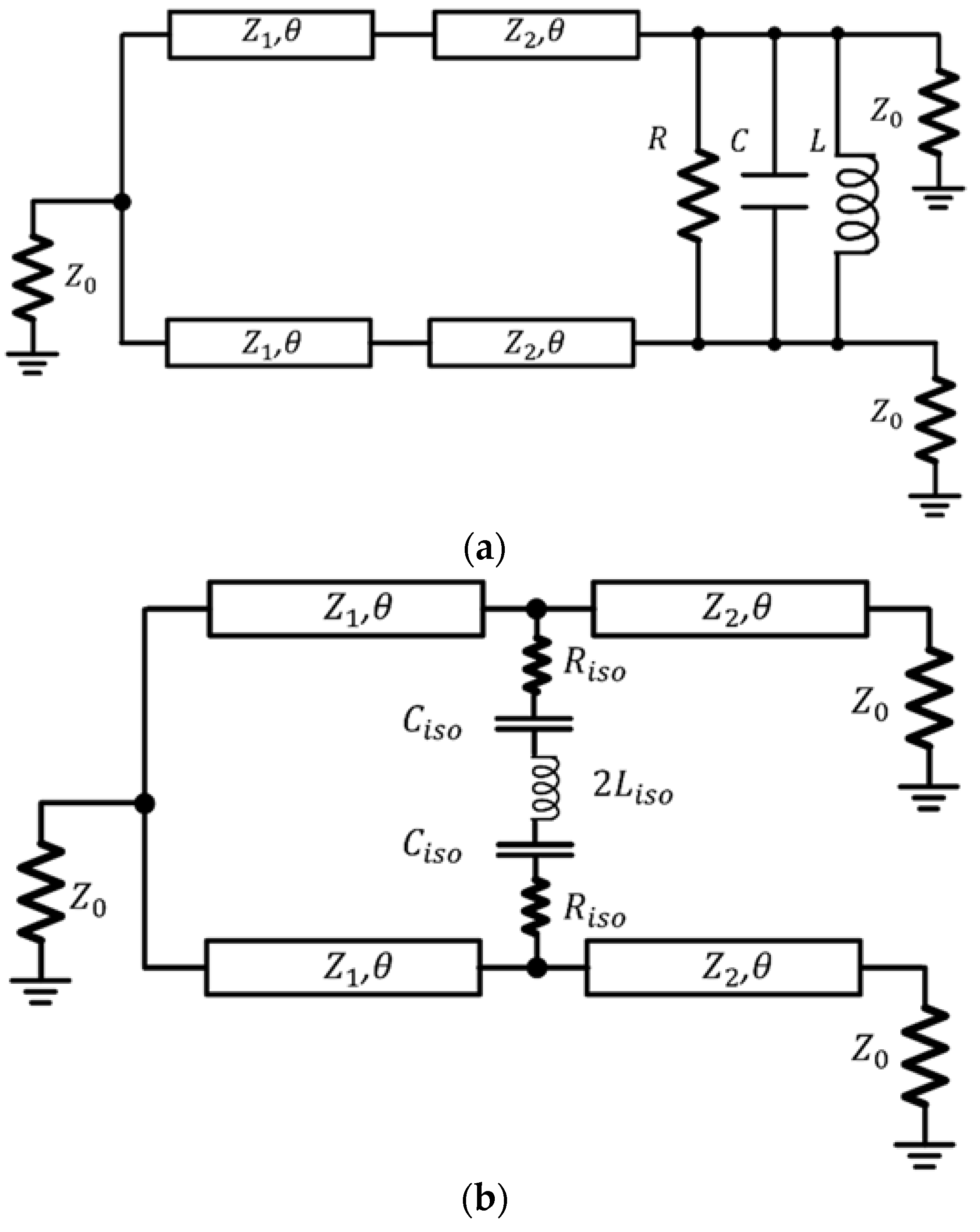
2. Design and Analysis

Figure 1b shows the configuration of the proposed power divider with series resistor–capacitor–inductor network adopted in the complex isolation network. Due to the symmetric nature of the geometry, analysis of such configuration is generally performed by placing either open-circuited or short-circuited bisecting plane at the plane of symmetry.

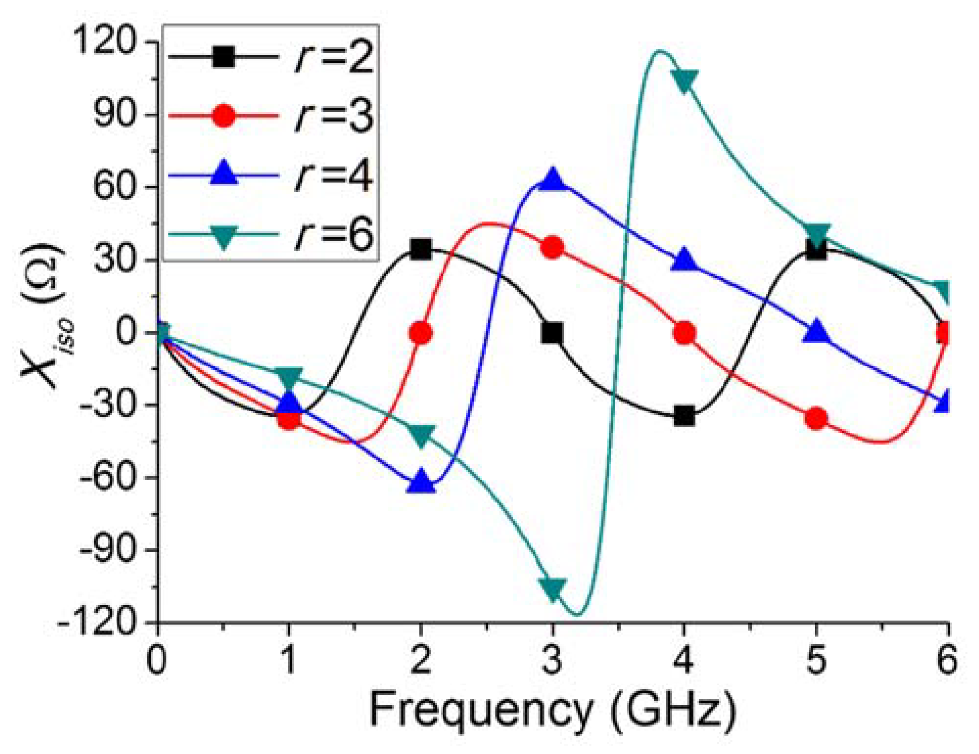
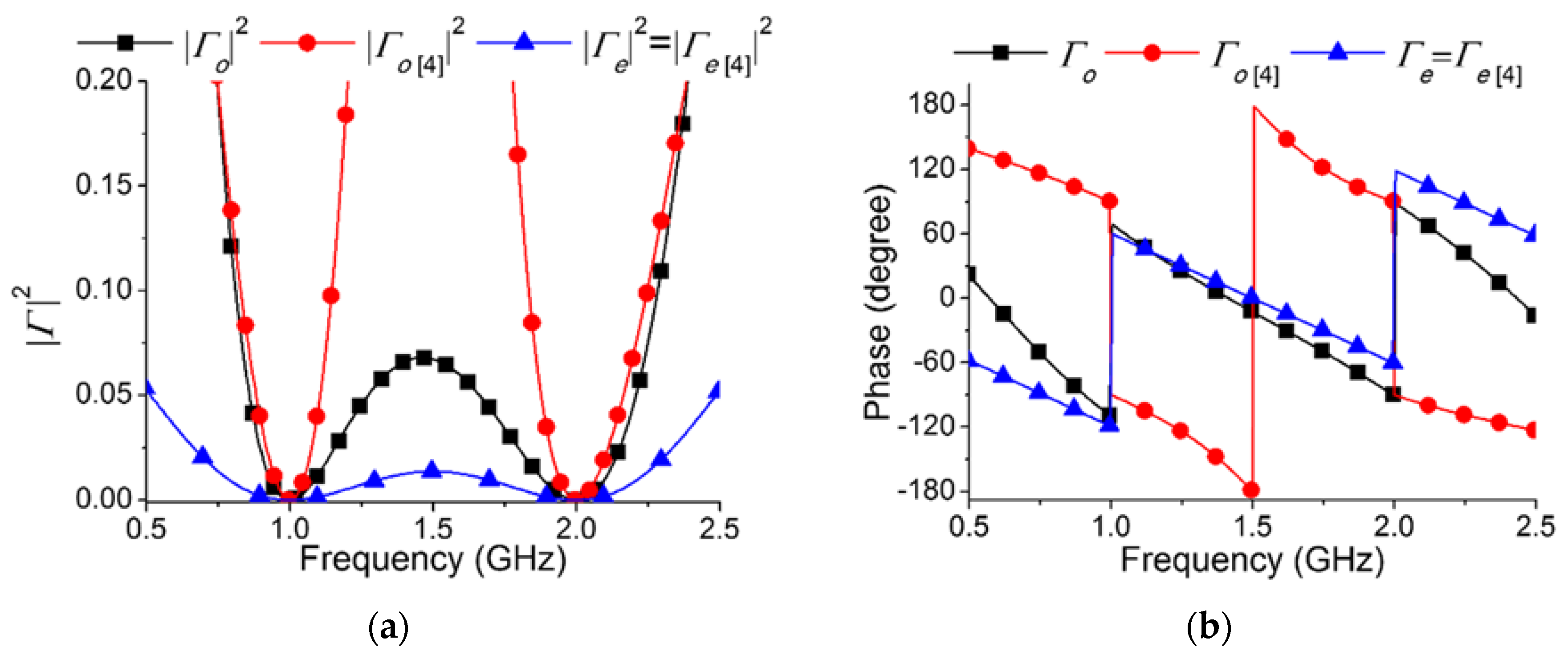
2.1. Even-Mode Analysis

The design starts with the determination of the frequency ratio, which determines the electrical lengths and characteristic impedance of four TLs [3]. The electrical length θ ( r ) , as well as the characteristic impedance Z 1 ( r ) and Z 2 ( r ) , can be defined as:
θ ( r ) = π 1 + r
Z 1 ( r ) = Z 0 c o t 2 ( θ ( r ) ) + c o t 4 ( θ ( r ) ) + 8 ,  
Z 2 ( r ) = 2 Z 0 Z 1 ( r )
Figure 2 shows the even-mode subnetwork when an open-circuit bisection is applied on the plane of symmetry.
In Equation (1), r denotes the frequency ratio, which is f 2 / f 1 , and θ is the electric length at f 1 . For impedance matching at the output port yielding to minimum flection, the even-mode operation satisfies the following conditions:
Z i n , e 1 ( r ) = Z 1 ( r ) 2 Z 0 + j Z 1 ( r ) t a n θ ( r ) Z 1 ( r ) + j 2 Z 0 t a n θ ( r )
Z i n , e 2 ( r ) = Z 2 ( r ) Z i n , e 1 ( r ) + j Z 2 ( r ) t a n θ ( r ) Z 2 ( r ) + j Z i n , e 1 ( r ) t a n θ ( r )  
Γ e ( r ) = Z i n , e 1 ( r ) Z 0 Z i n , e 1 ( r ) + Z 0

2.2. Odd-Mode Analysis

For the odd-mode analysis, a short-circuit bisecting plane instead was placed at the plane of symmetry. Figure 3 shows the odd-mode subnetwork after bisection.
A similar technique can be applied by adopting an INW between two TLs, leading to the odd-mode subnetwork. Imposing the same condition for impedance matching at the output port yields the following governing equations to synthesize the complex isolation Z i s o ( f , r ) .
Z i s o ( r ) = R i s o ( r ) + j X i s o ( r )  
Z i n , o 1 ( r ) = [ 1 Z i s o ( r ) + 1 j Z 1 ( r ) t a n θ ( r ) ] 1
Z i n , o 2 ( r ) = Z 2 ( r ) Z i n , o 1 ( r ) + j Z 2 ( r ) t a n θ ( r ) Z 2 ( r ) + j Z i n , o 1 ( r ) t a n θ ( r )
Γ o ( r ) = Z i n , o 2 ( r ) Z 0 Z i n , o 2 ( r ) + Z 0
The real and imaginary parts of the impedance Ziso can be equated as:
R i s o ( r ) = Z 0 Z 1 ( r ) 2 Z 2 ( r ) 2 t a n 2 θ ( r ) / c o s 2 θ ( r ) [ Z 0 ( Z 1 ( r ) t a n 2 θ ( r ) Z 2 ( r ) ) ] 2 + [ Z 2 ( r ) t a n θ ( r ) ( Z 1 ( r ) + Z 2 ( r ) ) ] 2
X i s o ( r ) = Z 1 ( r ) Z 2 ( r ) [ t a n 2 θ ( r ) ( Z 0 2 Z 1 ( r ) Z 1 ( r ) Z 1 ( r ) 2 Z 1 ( r ) 3 ) Z 0 2 Z 2 ( r ) ] c o t θ ( r ) { [ Z 0 ( Z 1 ( r ) t a n 2 θ ( r ) Z 2 ( r ) ) ] 2 + [ Z 2 ( r ) t a n θ ( r ) ( Z 1 ( r ) + Z 2 ( r ) ) ] 2 }
Figure 4 plots the frequency dependence for the imaginary parts of the Ziso at different frequency ratios r. For the sake of simplicity, the fundamental frequency was set at 1 GHz. Clearly, the frequency dependence of Xiso exhibited capacitive characteristic at the fundamental frequency and inductive at the higher one. This suggests that a series L-C configuration should be adopted in the INW. Additionally, the resonance frequency of the L-C tank should be designed between the center frequency of the two desired bands to accommodate for the change from the capacitive to the inductive characteristics. This is the main reason that we adopted the configuration of INW shown in Figure 1b.
The corresponding inductance and capacitance in the complex INW can be synthesized as:
L i s o ( f 1 ,   r ) = f 1 X i s o ( f 1 , r ) f 1 r X i s o ( f 1 r , r ) 2 π ( f 1 2 ( f 1 r ) 2 )
C i s o ( f 1 , r ) = f 1 X i s o ( f 1 , r ) f 1 r X i s o ( f 1 r , r ) 2 π ( f 1 ( f 1 r ) 2 X i s o ( f 1 , r ) f 1 2 f 1 X i s o ( f 1 r , r ) )
Finally, the S-parameters of the DBPD can be related to the reflection coefficients as:
| S 11 | = | Γ e |
S 22 = Γ e + Γ o 2
S 23 = Γ e Γ o 2
Clearly, from Equation (15), the bandwidth of the even-mode reflection coefficient has direct impact on the impedance bandwidth at the common port. Moreover, the isolation is related to the difference of them. Since both Γ e and Γ o are complex quantities, the isolation will be less frequency-dependent if the phase difference between them is small. To show the effect of bandwidth improvement of our approach, a design was synthesized using the same frequency ratio of 2 as in [4]. The other parameters synthesized using the derived procedure are R i s o = 47.15   Ω , L i s o = 5.5   nH , and C i s o = 2.3   pF , respectively. The fundamental frequency f1 has been set to be 1 GHz.
Figure 5 shows the calculated magnitude and phase of the reflection coefficients for the even- and odd-mode bisected networks. The analysis results of the configuration in a previous study [4] are also included for comparison purposes. It is noted that the even-mode configurations for both structures are identical, so the responses are the same. As observed in Figure 5, the magnitude of the odd-mode reflection coefficient exhibited a less frequency-dependent behavior compared to that of a previous study [4]. Additionally, the phase difference between Γ e and Γ o is smaller. Both of these characteristics led to a better isolation performance in terms of level and bandwidth.
In order to check the applicability of the proposed design and synthesis procedure, DBPDs with different frequency ratios r have been designed. Figure 6 shows the simulated S-parameters of the designs with different frequency ratios. It is observed that all the designs exhibit good impedance bandwidth as well as isolation performance.

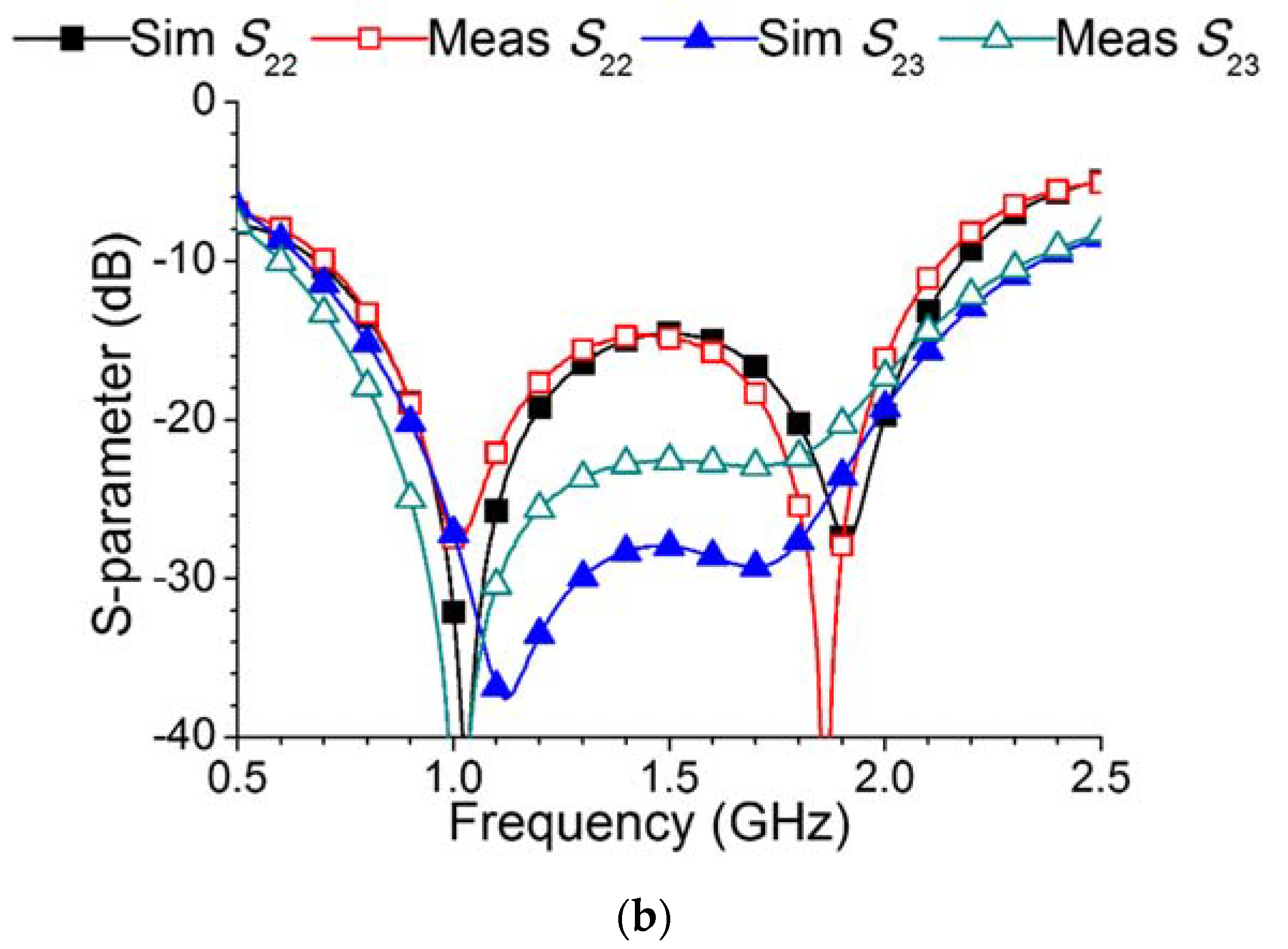
3. Experimental Verification

To validate the design equations and the effectiveness of the proposed configuration, a DBPD centered at 1 GHz and 2 GHz was designed, fabricated, and characterized for performance comparison, which is shown in Figure 7a. We started the synthesis procedure with a frequency ratio of 2. The fabrication process uses RO4003 substrate with a thickness of 0.508 mm, dielectric constant of 3.38, and loss tangent of 0.0027. The cascaded 2 inductors, 2 resistors, and single capacitor in the INW were synthesized to be two Standard 0402 surface-mount-type 5.6 nH, 47 Ω, and a 0603 surface-mount-type 1.2 pF chip device, respectively. Figure 7 shows the layout and the photograph of the fabricated prototype. The detailed parameters are listed in Table 1.
Figure 8 shows the measured and simulated S-parameters of the fabricated prototype. Because of the network symmetry, the return loss at port 3 is identical to that of port 2. In general, the simulation results agreed well with the measurements except minor frequency shift observed in the two dips of S11. The vector network analyzer with model number MS46522A from Anritsu was used for measurement. The performance of the prototype was compared against the previously published work as summarized in Table 2. The bandwidth of the corresponding S-parameters is defined at the corresponding magnitude being less than −20 dB. In some cases, the response exhibited a wideband performance. For some cases in other researches the level of the input return loss did not reach 20 dB, so the corresponding bandwidth was not defined. As observed in Table 2, the proposed configuration is the most compact-sized one with port separation. In general, the impedance bandwidth at the common port tends to be narrower for those configurations with more number of TLs. This is mainly due to the strong frequency-dependent nature of the parameters of TLs. On the contrary, for configurations with less TLs, simultaneous achievement of impedance bandwidth and size compactness was possible. As for the isolation performance, it is clear that the proposed topology exhibited a good isolation level and bandwidth, which could be attributed to the almost identical frequency-dependent characteristics of the even- and odd-mode reflection coefficients. This is in good agreement with the theoretical analysis.
For system applications, one of the key issues is definitely the practical operational bandwidth of the DBPD. Practically, the practical operational bandwidth should be defined as the intersections of the individual bandwidth of the corresponding S-parameters. Thus, such bandwidth would be the narrowest one among all the bandwidth of the individual S-parameters, which would usually be the impedance bandwidth of one of the ports. In this sense, the proposed configuration outperformed the others showing the widest practical bandwidth at both bands, which were measured to be 21.8% at 1 GHz and 9.6% at 2 GHz. Finally, the amplitude and phase imbalance characteristics were also measured and plotted in Figure 9. The proposed configuration demonstrated good performance with a phase imbalance of 0.134 degree (0.891 degree) and an amplitude of 0.038 dB (0.194 dB) measured at 1 GHz (2 GHz), respectively.

4. Conclusions

In this paper, we proposed a new configuration for the realization of a dual-band power divider, featuring complex isolation with port extension. Rigorous analysis has been performed and a new combination of the components in the complex isolation network was synthesized from the theoretical analysis. Measured responses of the fabricated prototype exhibited a practical operation bandwidth of 222 MHz and 173 MHz centered at 1 GHz and 2 GHz, respectively, with size compactness compared to previous publications.

Author Contributions

Conceptualization and methodology, H.-T.H. and T.-J.C.; software and validation, T.-J.C.; writing—original draft preparation, T.-J.C.; writing—review and editing, T.-J.H., Y.-F.T., H.-T.H., and T.-J.C.; supervision, project administration and funding acquisition, H.-T.H. All authors have read and agreed to the published version of the manuscript.

Funding

This research was funded by the Ministry of Science and Technology, Taiwan, under Grants 109-2221-E-009-059 and 109-2927-I-009-503. This research was also financially supported by the “Center for the Semiconductor Technology Research” from The Featured Areas Research Center Program within the framework of the Higher Education Sprout Project by the Ministry of Education (MOE) in Taiwan and also funded in part by the Ministry of Science and Technology, Taiwan, under Grant MOST-109-2634-F-009-029.

Conflicts of Interest

The authors declare no conflict of interest.

References

  1. Wilkinson, E.J. An N-Way Hybrid Power Dividers. IEEE Trans. Microw. Theory Tech. 1960, 8, 116–118. [Google Scholar] [CrossRef]
  2. Srisathit, S.; Chongcheawchamnan, M.; Worapishet, A. Design and realisation of dual-band 3 dB power divider based on two-section transmission-line topology. IET Electron. Lett. 2003, 39, 723–724. [Google Scholar] [CrossRef]
  3. Monzon, C. A small dual-frequency transformer in two sections. IEEE Trans. Microw. Theory Tech. 2003, 51, 1157–1161. [Google Scholar] [CrossRef]
  4. Wu, L.; Sun, Z.; Yilmaz, H.; Berroth, M. A dual-frequency wilkinson power divider. IEEE Trans. Microw. Theory Tech. 2006, 54, 278–284. [Google Scholar] [CrossRef]
  5. Gao, N.; Wu, G.; Tang, Q. Design of a Novel Compact Dual-Band Wilkinson Power Divider with Wide Frequency Ratio. IEEE Microw. Wirel. Compon. Lett. 2014, 24, 81–83. [Google Scholar] [CrossRef]
  6. Kawai, T.; Yamasaki, J.; Kokubo, Y.; Ohta, I. A design method of dual-frequency wilkinson power divider. In Proceedings of the 2006 IEEE MTT-S 2006 Asia-Pacific Microwave Conference, Yokohama, Japan, 12–15 December 2006; pp. 913–916. [Google Scholar]
  7. Park, M.; Lee, B. A Dual-Band Wilkinson Power Divider. IEEE Microw. Wirel. Compon. Lett. 2008, 18, 85–87. [Google Scholar] [CrossRef]
  8. Zhang, T.; Che, W.; Chen, H.; Feng, W. A Compact Four-way Dual-band Power Divider Using Lumped Elements. IEEE Microw. Wirel. Compon. Lett. 2015, 25, 94–96. [Google Scholar] [CrossRef]
  9. Ahmed, U.T.; Abbosh, A.M. Modified Wilkinson power divider using coupled microstrip lines and shunt open-ended stubs. IET Electron. Lett. 2015, 51, 838–839. [Google Scholar] [CrossRef]
  10. Park, M. Dual-Band Wilkinson Divider with Coupled Output Port Extensions. IEEE Trans. Microw. Theory Tech. 2009, 57, 2232–2237. [Google Scholar] [CrossRef]
  11. Antsos, D.; Crist, R.; Sukamto, L. A novel Wilkinson power divider with predictable performance at K and Ka-band. In Proceedings of the 1994 IEEE MTT-S International Microwave Symposium Digest, San Diego, CA, USA, 23–27 May 1994; pp. 907–910. [Google Scholar]
  12. Horst, S.; Bairavasubramanian, R.; Tentzeris, M.; Papapolymerou, J. Modified Wilkinson power dividers for millimeter-wave integrated circuits. IEEE Trans. Microw. Theory Tech. 2007, 55, 2439–2446. [Google Scholar] [CrossRef]
  13. Cheng, K.-K.M.; Law, C. A novel approach to the design and implementation of dual-band power divider. IEEE Trans. Microw. Theory Tech. 2008, 56, 487–492. [Google Scholar] [CrossRef]
  14. Shin, Y.; Lee, B.; Park, M.-J. Dual-band Wilkinson power divider with shifted output ports. IEEE Microw. Wirel. Compon. Lett. 2008, 18, 443–445. [Google Scholar] [CrossRef]
  15. Li, X.; Yang, Y.-J.; Yang, L.; Gong, S.-X.; Hong, T.; Chen, X.; Zhang, Y.-J. Design of unequal Wilkinson power divider for dual-band operation with isolation stubs. IET Electron. Lett. 2009, 45, 1245–1247. [Google Scholar] [CrossRef]
  16. Wu, G.; Yang, L.; Zhou, Y.; Xu, Q. Wilkinson power divider design for dual-band applications. IET Electron. Lett. 2014, 50, 1003–1005. [Google Scholar] [CrossRef]
  17. Maktoomi, M.-A.; Hashmi, M.-S. A performance enhanced port extended dual-band Wilkinson power divider. IEEE Access 2017, 5, 11832–11840. [Google Scholar] [CrossRef]
  18. Park, M.-J.; Lee, B. Wilkinson power divider with extended ports for dual-band operation. IET Electron. Lett. 2008, 44, 916–918. [Google Scholar] [CrossRef]
  19. Wu, Y.; Liu, Y.; Li, S. Unequal dual-frequency Wilkinson power divider including series resistor-inductor-capacitor isolation structure. IET Microw. Antennas Propag. 2009, 3, 1079–1085. [Google Scholar] [CrossRef]
  20. Ahn, S.; Lee, J.W.; Cho, C.S.; Lee, T.K. A Dual-Band Unequal Wilkinson Power Divider with Arbitrary Frequency Ratios. IEEE Microw. Wirel. Compon. Lett. 2009, 19, 783–785. [Google Scholar] [CrossRef]
  21. Gharehaghaji, H.S.; Shamsi, H. Design of Unequal Dual Band Gysel Power Divider with Isolation Bandwidth Improvement. IEEE Microw. Wirel. Compon. Lett. 2017, 27, 138–140. [Google Scholar] [CrossRef]
  22. Pang, Y.-H.; Li, Z.-H. Dual-band bandpass Wilkinson power divider of controllable bandwidths. IET Electron. Lett. 2016, 52, 537–539. [Google Scholar] [CrossRef]
  23. Wang, X.; Ma, Z.; Ohira, M. Theory and Experiment of Two-Section Two-Resistor Wilkinson Power Divider with Two Arbitrary Frequency Bands. IEEE Trans. Microw. Theory Tech. 2018, 66, 1291–1300. [Google Scholar] [CrossRef]
  24. Wang, X.; Sakagami, I.; Takahashi, K.; Okamura, S. A Generalized Dual-Band Wilkinson Power Divider with Parallel L, C, and R Components. IEEE Trans. Microw. Theory Tech. 2012, 60, 952–964. [Google Scholar] [CrossRef]
  25. Liu, F.; Lee, J. Design of New Dual-Band Wilkinson Power Dividers with Simple Structure and Wide Isolation. IEEE Trans. Microw. Theory Tech. 2019, 67, 3628–3635. [Google Scholar] [CrossRef]
  26. Mirzaei, M.; Sheikhi, A. Design and implementation of microstrip dual-band filtering power divider using square-loop resonator. IET Electron. Lett. 2020, 56, 19–21. [Google Scholar] [CrossRef]
  27. Wang, X.; Wang, J.; Zhang, G.; Hong, J.; Wu, W. Dual-Wideband Filtering Power Divider With Good Isolation and High Selectivity. IEEE Microw. Wirel. Compon. Lett. 2017, 27, 1071–1073. [Google Scholar] [CrossRef]
  28. Maktoomi, M.H.; Banerjee, D.; Hashmi, M.S. An Enhanced Frequency-Ratio Coupled-Line Dual-Frequency Wilkinson Power Divider. IEEE Trans. Circuits Syst. II Exp. Briefs 2018, 65, 888–892. [Google Scholar] [CrossRef]
Figure 1. (a) The conventional dual-band power divider and (b) our proposed dual-band power divider.
Electronics 09 02192 g001
Figure 2. Bisected network with open-circuit bisecting plane at the plane of symmetry for even-mode analysis.
Electronics 09 02192 g002
Figure 3. Bisected network with short-circuit bisecting plane at the plane of symmetry for odd-mode analysis.
Electronics 09 02192 g003
Figure 4. Frequency dependence of Xiso under various frequency ratios r with the fundamental frequency set at 1 GHz.
Electronics 09 02192 g004
Figure 5. The (a) magnitude and (b) phase of the even- and odd-mode reflection coefficients for this work and a previous study [4].
Electronics 09 02192 g005
Figure 6. The simulated S-parameters of various designs with different frequency ratios to show the applicability of the proposed approach.
Electronics 09 02192 g006
Figure 7. The (a) layout and (b) fabricated prototype of the dual-band power divider for verification.
Electronics 09 02192 g007
Figure 8. Measured and simulated (a) S 11 , S 12 , (b) S 22 , and S 23 of the fabricated prototype.
Electronics 09 02192 g008aElectronics 09 02192 g008b
Figure 9. Measured phase and amplitude imbalance of the fabricated prototype.
Electronics 09 02192 g009
Table 1. Design parameter of fabricated parameters for 1-GHz and 2-GHz dual-band power divider.
Z 1   ( Ω ) Z 2   ( Ω ) θ   ( degree ) R   ( Ω ) L   ( nH ) C   ( pF )
796360475.61.2
Table 2. Performance comparison of the fabricated prototype with previous publications.
Ref. f 2   ( G H z ) f 1   ( G H z ) Bandwidth (MHz)Insertion Loss
(dB)
Size 1Port Extension
S 11 S 22 S 23
f 1 f 2 f 1 f 2 f 1 f 2 f 1 f 2
[13] 2 1 4151519261713.83.6 5 λ 1 6   2Yes
[14] 2 1 38- 3477556853.33.6 5 λ 1 / 6 Yes
[21] 2 1 5010010012512001.92/5.01 42.14/5.24 42 λ 1 Yes
[22] 5.8 2.45 172238125- 3129973.84.22 λ 1 Yes
[23] 3.7 2.3 - 3N/A16013003.84.2>1.5 λ 1 No
[24] 5.3 3.1 - 3N/A891073.94.01.5 λ 1 No
[25] 1.8 0.9 12976327893153683.153.18 2 λ 1 / 3 No
[26] 12 3 11678333000783145010003.873.97 2 λ 1 / 5 No
[27] 3.5 1 - 33503253006503.283.35 5 λ 1 / 9 No
[28] 2 1 2003002002802502853.13.2 7 λ 1 / 6 No
This work 2 1 66256822217310743.143.19 2 λ 1 / 3 Yes
1 Sum of total length of the TLs used 2   λ 1 = electrical wavelength at f 1 . 3 Return loss does not reach 20-dB level. 4 Unequal power division ( S 21 / S 13 ).
Publisher’s Note: MDPI stays neutral with regard to jurisdictional claims in published maps and institutional affiliations.

