Ka-Band Diplexer for 5G mmWave Applications in Inverted Microstrip Gap Waveguide Technology


Abstract
:1. Introduction
2. Diplexer Design
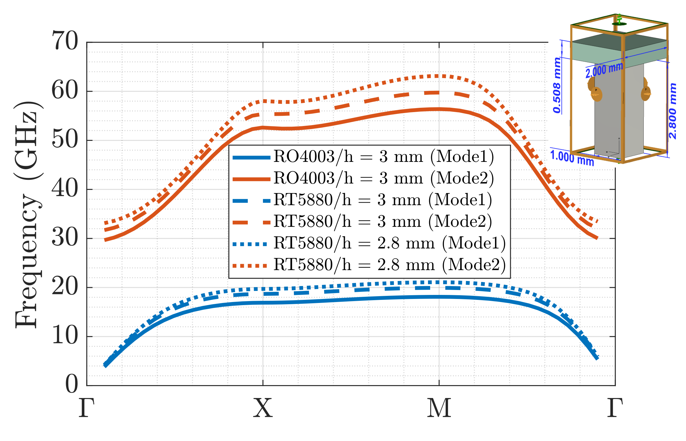
2.1. Selection of the Bed of Nails
2.2. Filters Design
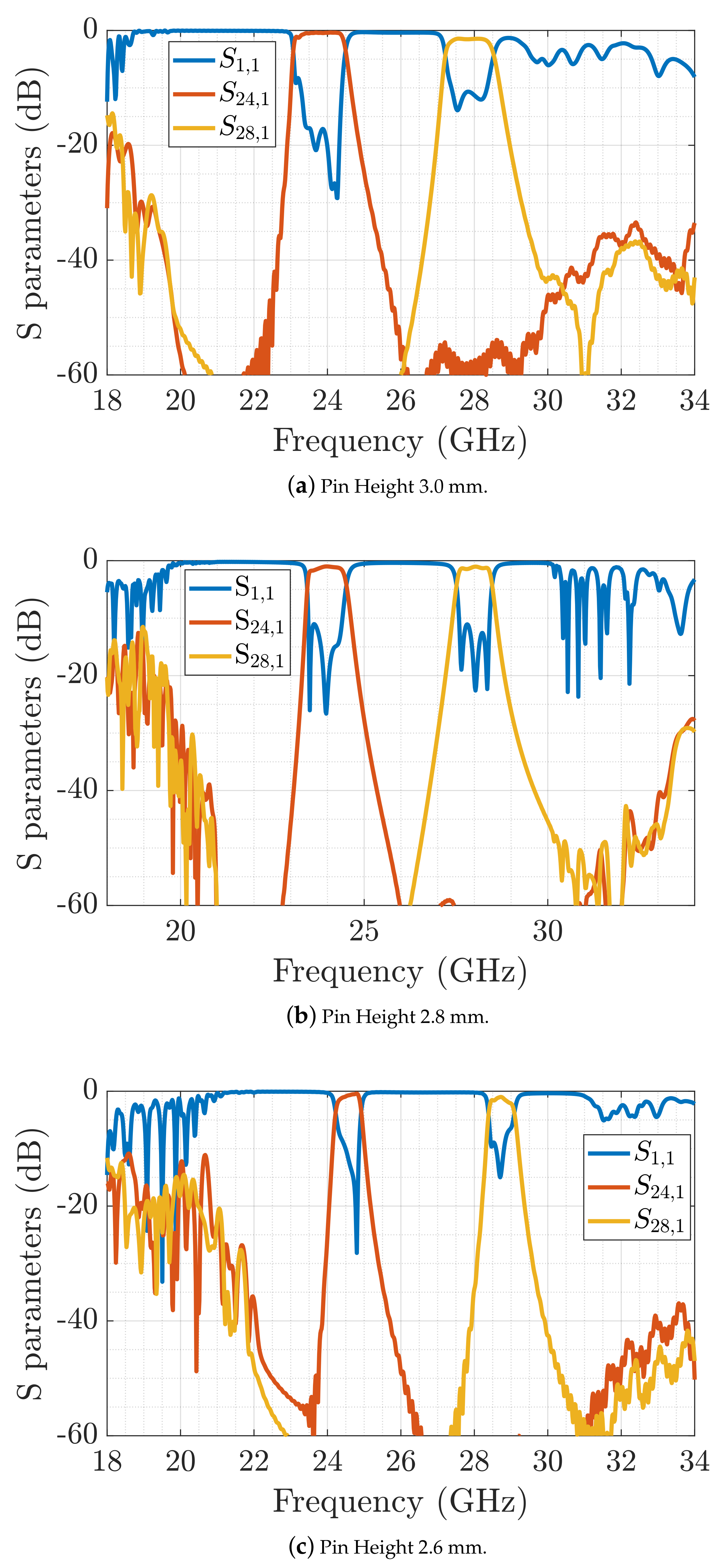
2.3. Diplexer Design
2.4. Inverted Microstrip Gap to Microstrip Transition Design
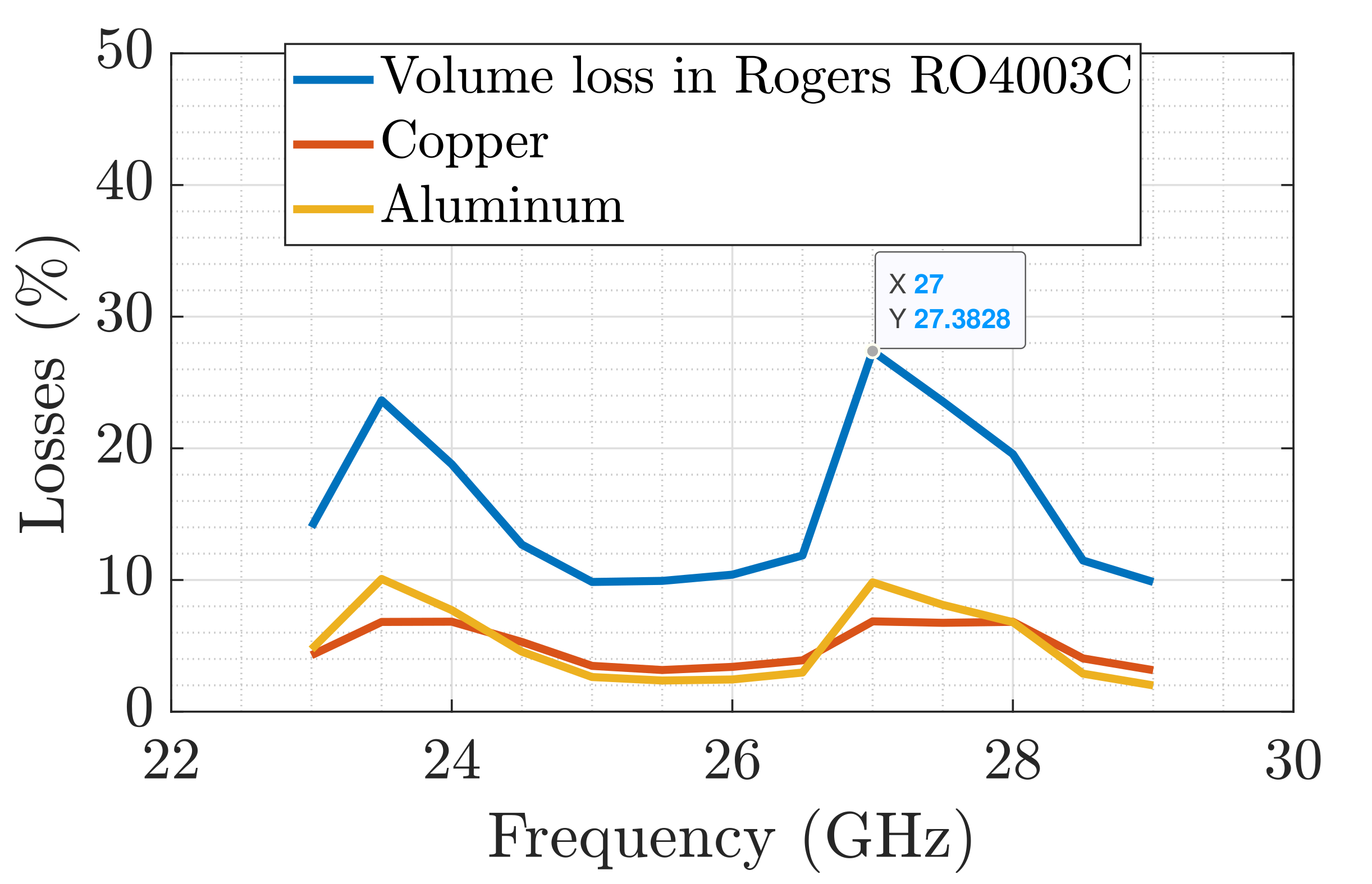
2.5. Losses Study
2.6. Low Loss RogersTM 5880 Substrate Design
3. Mechanical Design, Fabrication and Measurement
Comparison with Other Measured Diplexers
4. Conclusions
Author Contributions
Funding
Conflicts of Interest
Abbreviations
| AMC | Artificial Magnetic Conductor |
| CST | Computer Simulation Studio |
| PMC | Perfect Magnetic Conductor |
| TEM | Transverse Electromagnetic Mode |
References
- Kildal, P.; Alfonso, E.; Valero-Nogueira, A.; Rajo-Iglesias, E. Local Metamaterial-Based Waveguides in Gaps Between Parallel Metal Plates. IEEE Antennas Wirel. Propag. Lett. 2009, 8, 84–87. [Google Scholar] [CrossRef]
- Kildal, P.; Zaman, A.U.; Rajo-Iglesias, E.; Alfonso, E.; Valero-Nogueira, A. Design and experimental verification of ridge gap waveguide in bed of nails for parallel-plate mode suppression. IET Microw. Antennas Propag. 2011, 5, 262–270. [Google Scholar] [CrossRef]
- Rajo-Iglesias, E.; Zaman, A.U.; Kildal, P. Parallel Plate Cavity Mode Suppression in Microstrip Circuit Packages Using a Lid of Nails. IEEE Microw. Wirel. Components Lett. 2010, 20, 31–33. [Google Scholar] [CrossRef]
- Rajo-Iglesias, E.; Kildal, P. Numerical studies of bandwidth of parallel-plate cut-off realised by a bed of nails, corrugations and mushroom-type electromagnetic bandgap for use in gap waveguides. IET Microw. Antennas Propag. 2011, 5, 282–289. [Google Scholar] [CrossRef] [Green Version]
- Berenguer, A.; Baquero-Escudero, M.; Sanchez-Escuderos, D.; Vico, F. Suspended-strip gap waveguide coupled-line properties for Ka-band component design. In Proceedings of the 2015 9th European Conference on Antennas and Propagation (EuCAP), Lisbon, Portugal, 13–17 April 2015; pp. 1–5. [Google Scholar]
- Pucci, E.; Zaman, A.U.; Rajo-Iglesias, E.; Kildal, P. New low loss inverted microstrip line using gap waveguide technology for slot antenna applications. In Proceedings of the 5th European Conference on Antennas and Propagation (EUCAP), Rome, Italy, 11–15 April 2011; pp. 979–982. [Google Scholar]
- Pucci, E.; Rajo-Iglesias, E.; Kildal, P. New Microstrip Gap Waveguide on Mushroom-Type EBG for Packaging of Microwave Components. IEEE Microw. Wirel. Components Lett. 2012, 22, 129–131. [Google Scholar] [CrossRef] [Green Version]
- Liu, J.; Yang, J.; Zaman, A.U. Study of Dielectric Loss and Conductor Loss among Microstrip, covered Microstrip and inverted Microstrip Gap Waveguide utilizing variational Method in Millimeter Waves. In Proceedings of the 2018 International Symposium on Antennas and Propagation (ISAP), Busan, Korea, 23–26 October 2018; pp. 1–2. [Google Scholar]
- Rajo-Iglesias, E.; Ferrando-Rocher, M.; Zaman, A.U. Gap Waveguide Technology for Millimeter-Wave Antenna Systems. IEEE Commun. Mag. 2018, 56, 14–20. [Google Scholar] [CrossRef] [Green Version]
- Liu, J.; Yang, J.; Zaman, A.U. Analytical Solutions to Characteristic Impedance and Losses of Inverted Microstrip Gap Waveguide Based on Variational Method. IEEE Trans. Antennas Propag. 2018, 66, 7049–7057. [Google Scholar] [CrossRef] [Green Version]
- Pizarro, F.; Sanchez-Cabello, C.; Vazquez-Roy, J.L.; Rajo-Iglesias, E. Considerations of impedance sensitivity and losses in designing inverted microstrip gap waveguides. AEU Int. J. Electron. Commun. 2020, 124, 153353. [Google Scholar] [CrossRef]
- Brazález, A.A.; Iglesias, E.R.; Kildal, P. Investigation of transitions for use in inverted microstrip gap waveguide antenna arrays. In Proceedings of the The 8th European Conference on Antennas and Propagation (EuCAP 2014), The Hague, The Netherlands, 6–11 April 2014; pp. 995–999. [Google Scholar] [CrossRef] [Green Version]
- Brazález, A.A.; Rajo-Iglesias, E.; Vázquez-Roy, J.L.; Vosoogh, A.; Kildal, P. Design and Validation of Microstrip Gap Waveguides and Their Transitions to Rectangular Waveguide, for Millimeter-Wave Applications. IEEE Trans. Microw. Theory Tech. 2015, 63, 4035–4050. [Google Scholar] [CrossRef] [Green Version]
- Brazález, A.A.; Rajo-Iglesias, E.; Kildal, P. Design of millimeter-wave wideband gap waveguide transitions considering integration into the antenna system. In Proceedings of the 2015 9th European Conference on Antennas and Propagation (EuCAP), Lisbon, Portugal, 13–17 April 2015; pp. 1–5. [Google Scholar]
- Rajo-Iglesias, E.; Brazález, A.A. 5G antenna in inverted microstrip gap waveguide technology including a transition to microstrip. In Proceedings of the 2016 International Symposium on Antennas and Propagation (ISAP), Okinawa, Japan, 24–28 October 2016; pp. 1042–1043. [Google Scholar]
- Liu, J.; Zaman, A.U.; Kildal, P. Design of transition from WR-15 to inverted microstrip gap waveguide. In Proceedings of the 2016 Global Symposium on Millimeter Waves (GSMM) ESA Workshop on Millimetre-Wave Technology and Applications, Espoo, Finland, 6–8 June 2016; pp. 1–4. [Google Scholar] [CrossRef] [Green Version]
- Jinlin, L.; Zaman, A.U.; Kildal, P. Optimizing the numerical port for inverted microstrip gap waveguide in full-wave simulators. In Proceedings of the 2016 10th European Conference on Antennas and Propagation (EuCAP), Davos, Switzerland, 10–15 April 2016; 5. [Google Scholar] [CrossRef] [Green Version]
- Pucci, E.; Kildal, P.; Rajo-Iglesias, E.; Vazquez-Roy, J. Design of a four-element horn antenna array fed by inverted microstrip gap waveguide. In Proceedings of the 2013 IEEE Antennas and Propagation Society International Symposium (APSURSI), Orlando, FL, USA, 7–13 July 2013; pp. 1226–1227. [Google Scholar] [CrossRef]
- Sanchez-Cabello, C.; Rajo-Iglesias, E. Low cost self-diplexed antenna in inverted microstrip gap waveguide technology. In Proceedings of the 2014 International Symposium on Antennas and Propagation Conference Proceedings, Kaohsiung, Taiwan, 2–5 December 2014; pp. 169–170. [Google Scholar] [CrossRef]
- Pucci, E.; Rajo-Iglesias, E.; Vázquez-Roy, J.; Kildal, P. Planar Dual-Mode Horn Array With Corporate-Feed Network in Inverted Microstrip Gap Waveguide. IEEE Trans. Antennas Propag. 2014, 62, 3534–3542. [Google Scholar] [CrossRef] [Green Version]
- Razavi, S.A.; Kildal, P. An air-filled cavity-backed 2 × 2 slot sub-array fed by inverted microstrip gap waveguide. In Proceedings of the 2015 9th European Conference on Antennas and Propagation (EuCAP), Lisbon, Portugal, 13–17 April 2015; pp. 1–4. [Google Scholar]
- Liu, J.; Vosoogh, A.; Zaman, A.U.; Kildal, P. Design of a cavity-backed slot array unit cell on inverted microstrip gap waveguide. In Proceedings of the 2015 International Symposium on Antennas and Propagation (ISAP), Hobart, TAS, Australia, 9–12 November 2015; pp. 1–4. [Google Scholar]
- Sanchez-Cabello, C.; Rajo-Iglesias, E. Optimized self-diplexed antenna in gap waveguide technology. In Proceedings of the 2015 IEEE International Symposium on Antennas and Propagation USNC/URSI National Radio Science Meeting, Vancouver, BC, Canada, 19–24 July 2015; pp. 460–461. [Google Scholar] [CrossRef]
- Liu, J.; Vosoogh, A.; Zaman, A.U.; Kildal, P. Design of 8 x 8 slot array antenna based on inverted microstrip gap waveguide. In Proceedings of the 2016 International Symposium on Antennas and Propagation (ISAP), Okinawa, Japan, 24–28 October 2016; pp. 760–761. [Google Scholar]
- Zaman, A.U.; Kildal, P. Different gap waveguide slot array configurations for mmwave fixed beam antenna application. In Proceedings of the 2016 10th European Conference on Antennas and Propagation (EuCAP), Davos, Switzerland, 10–15 April 2016; pp. 1–4. [Google Scholar] [CrossRef] [Green Version]
- Liu, J.; Vosoogh, A.; Zaman, A.U.; Yang, J. Design and Fabrication of a High-Gain 60-GHz Cavity-Backed Slot Antenna Array Fed by Inverted Microstrip Gap Waveguide. IEEE Trans. Antennas Propag. 2017, 65, 2117–2122. [Google Scholar] [CrossRef]
- Liu, J.; Vosoogh, A.; Zaman, A.U.; Yang, J. Slot antenna array unit cell directly fed by inverted microstrip gap waveguide. In Proceedings of the 2017 International Symposium on Antennas and Propagation (ISAP), Phuket, Thailand, 30 October–2 November 2017; pp. 1–2. [Google Scholar] [CrossRef] [Green Version]
- Cao, J.; Wang, H.; Mou, S.; Liu, S. W-band High-Performance Cavity-backed Slot Antenna Array with Inverted Microstrip Gap Waveguide. In Proceedings of the 2018 IEEE International Symposium on Antennas and Propagation USNC/URSI National Radio Science Meeting, Boston, MA, USA, 8–13 July 2018; pp. 1039–1040. [Google Scholar] [CrossRef]
- Liu, J.; Zaman, A.U.; Yang, J. A Low Sidelobe Double-Layer Corporate-Feed Array Antenna by Inverted Microstrip Gap Waveguide at 28 GHz. In Proceedings of the 2019 International Symposium on Antennas and Propagation (ISAP), Xi’an, China, 27–30 October 2019; pp. 1–4. [Google Scholar]
- Zhang, T.; Chen, L.; Moghaddam, S.M.; Uz Zaman, A.; Yang, J. Ultra-wideband Circularly Polarized Planar Array Antenna Using Single-Arm-Spiral Elements and Dielectric-based IMGW. In Proceedings of the 2019 International Symposium on Antennas and Propagation (ISAP), Xi’an, China, 27–30 October 2019; pp. 1–3. [Google Scholar]
- Zhang, T.; Chen, L.; Moghaddam, S.M.; Uz Zaman, A.; Yang, J. Wideband Dual-polarized Array Antenna on Dielectric-based Inverted Microstrip Gap Waveguide. In Proceedings of the 2019 13th European Conference on Antennas and Propagation (EuCAP), Krakow, Poland, 31 March–5 April 2019; pp. 1–3. [Google Scholar]
- Zhang, T.; Chen, L.; Moghaddam, S.M.; Zaman, A.U.; Yang, J. Ultra-wideband linearly polarised planar bowtie array antenna with feeding network using dielectric-based inverted microstrip gap waveguide. IET Microw. Antennas Propag. 2020, 14, 485–490. [Google Scholar] [CrossRef]
- Algaba-Brazalez, A.; Rajo-Iglesias, E. Design of a Butler matrix at 60 GHz in inverted microstrip gap waveguide technology. In Proceedings of the 2015 IEEE International Symposium on Antennas and Propagation USNC/URSI National Radio Science Meeting, Vancouver, BC, Canada, 19–24 July 2015; pp. 2125–2126. [Google Scholar] [CrossRef] [Green Version]
- Pizarro, F.; Ramírez-Gil, D.; Algaba-Brazález, A.; Herrán-Ontanón, L.F.; Rajo-Iglesias, E. Comparison study of 4 × 4 Butler matrices in microstrip technologies for Ka-band. AEU Int. J. Electron. Commun. 2020, 122, 153248. [Google Scholar] [CrossRef]
- Sorkherizi, M.S.; Kishk, A.A. Lowloss planar bandpass filters for millimeter-wave application. In Proceedings of the 2015 IEEE MTT-S International Microwave Symposium, Phoenix, AZ, USA, 17–22 May 2015; pp. 1–4. [Google Scholar] [CrossRef]
- Vosoogh, A.; Brazález, A.A.; Kildal, P. A V-Band Inverted Microstrip Gap Waveguide End-Coupled Bandpass Filter. IEEE Microw. Wirel. Components Lett. 2016, 26, 261–263. [Google Scholar] [CrossRef]
- Sharifi Sorkherizi, M.; Kishk, A.A. Fully Printed Gap Waveguide With Facilitated Design Properties. IEEE Microw. Wirel. Components Lett. 2016, 26, 657–659. [Google Scholar] [CrossRef]
- Inclan-Sanchez, L.; Sanchez-Cabello, C.; Vazquez-Roy, J.L.; Rajo-Iglesias, E. New EBG-filter design in inverted microstrip gap waveguide technology. In Proceedings of the 2017 IEEE International Symposium on Antennas and Propagation USNC/URSI National Radio Science Meeting, San Diego, CA, USA, 9–14 July 2017; pp. 1663–1664. [Google Scholar] [CrossRef]
- Deng, J.; Li, M.; Sun, D.; Guo, L.; Ma, X. Compact Dual-Band Inverted-Microstrip Ridge Gap Waveguide Bandpass Filter. IEEE Trans. Microw. Theory Tech. 2020, 68, 2625–2632. [Google Scholar] [CrossRef]
- Vosoogh, A.; Sorkherizi, M.S.; Zaman, A.U.; Yang, J.; Kishk, A.A. An Integrated Ka-Band Diplexer-Antenna Array Module Based on Gap Waveguide Technology With Simple Mechanical Assembly and No Electrical Contact Requirements. IEEE Trans. Microw. Theory Tech. 2018, 66, 962–972. [Google Scholar] [CrossRef]
- Lowpass and Bandpass Filters. In Microstrip Filters for RF/Microwave Applications; John Wiley & Sons, Inc.: Hoboken, NJ, USA, 2011; pp. 112–161. [CrossRef]
- Jung, D.; Chang, K. Microstrip diplexer design for X-band RF/microwave front-end applications. In Proceedings of the 2011 IEEE International Symposium on Antennas and Propagation (APSURSI), Spokane, WA, USA, 3–8 July 2011; pp. 5–7. [Google Scholar] [CrossRef]
- Zhao, W.; Zhang, Y.; Guo, Y. A novel Ka-band bandpass filter using microstrip closed loop resonators. In Proceedings of the 2009 Asia Pacific Microwave Conference, Singapore, 7–10 December 2009; pp. 1443–1445. [Google Scholar] [CrossRef]
- Zhang, Q.; Dong, Y.; Cao, J. Dual-mode bandpass filter using microstrip SIR at Ka band. In Proceedings of the 2009 Asia Pacific Microwave Conference, Singapore, 7–10 December 2009; pp. 1401–1404. [Google Scholar] [CrossRef]
- Mbeutcha, M.; Johansen, T.K.; Dong, Y.; Cimoli, B.; Krozer, V. Replicability of a Millimeter-Wave Microstrip Bandpass Filter using Parallel Coupled Lines. In Proceedings of the 2018 IEEE MTT-S Latin America Microwave Conference (LAMC 2018), Arequipa, Peru, 12–14 December 2018; pp. 1–3. [Google Scholar] [CrossRef]
- Keskin, A.K.; Dagcan Senturk, M.; Demirel, S.; Kizilay, A.; Turk, A.S. Front-end design for Ka band mm-Wave radar. In Proceedings of the 2016 17th International Radar Symposium (IRS), Krakow, Poland, 10–12 May 2016; pp. 1–4. [Google Scholar] [CrossRef]
- Liu, Z.; Zhang, R.; Hua, T. Design of Ka-band practical waveguide duplexer. In Proceedings of the 2016 CIE International Conference on Radar (RADAR), Guangzhou, China, 10–13 October 2016; pp. 1–3. [Google Scholar] [CrossRef]
- Ashiq, I.; Khanna, A. A novel ultra-broadband DC-36-to-66-GHz hybrid diplexer using waveguide and SSL technology. In Proceedings of the 2014 44th European Microwave Conference, Rome, Italy, 6–9 October 2014; pp. 1111–1114. [Google Scholar] [CrossRef]
- Setoodeh, S.; Mansour, R.R.; Gupta, D. Multi-layer low temperature superconducting K-band filter and diplexer design. In Proceedings of the 2013 IEEE MTT-S International Microwave Symposium Digest (MTT), Seattle, WA, USA, 2–7 June 2013; pp. 1–4. [Google Scholar] [CrossRef]
- Brown, A.R.; Rebeiz, G.M. A high-performance integrated K-band diplexer. IEEE Trans. Microw. Theory Tech. 1999, 47, 1477–1481. [Google Scholar] [CrossRef]
- Bairavasubramanian, R.; Pinel, S.; Laskar, J.; Papapolymerou, J. Compact 60-GHz bandpass filters and duplexers on liquid crystal polymer technology. IEEE Microw. Wirel. Components Lett. 2006, 16, 237–239. [Google Scholar] [CrossRef]
- Rezaee, M.; Zaman, A.U. Realisation of carved and iris groove gap waveguide filter and E-plane diplexer for V-band radio link application. IET Microwaves Antennas Propag. 2017, 11, 2109–2115. [Google Scholar] [CrossRef]
- Hong, S.; Chang, K. Stub-tuned microstrip bandpass filters for millimeter-wave diplexer design. IEEE Microw. Wirel. Components Lett. 2005, 15, 582–584. [Google Scholar] [CrossRef]
- Wang, D.; Chin, K.; Che, W.; Chang, C.; Wu, Y. 60 GHz duplexer design using dual-mode SIW filters with single-sided transmission zeros. Electron. Lett. 2014, 50, 1529–1531. [Google Scholar] [CrossRef]
- Zurek, P.; Cappello, T.; Popovic, Z. Broadband Diplexed Power Amplifier. IEEE Microw. Wirel. Components Lett. 2020, 30, 1073–1076. [Google Scholar] [CrossRef]
- Rezaei, A.; Noori, L. Miniaturized microstrip diplexer with high performance using a novel structure for wireless L-band applications. Wirel. Netw. 2020, 26, 1795–1802. [Google Scholar] [CrossRef]


| Substrate | h pin | Finf (GHz) | Fsup (GHz) |
|---|---|---|---|
| RO4003C | 3 mm | 18.10 | 29.66 |
| RT5880 | 3 mm | 19.93 | 31.70 |
| RT5880 | 2.8 mm | 21.07 | 33.12 |
| f0 (GHz) | IL (dB) | Isol (dB) | BW (%) | Cost | Type | |
|---|---|---|---|---|---|---|
| [47] | 35 | 0.35 | NA | 1.7 | High | Waveguide |
| [48] | 66 | 1.5 | 50 | 59 | Very High | Waveguide + SSL |
| [49] | 20 | 4 | 50 | 2.4 | Very High | Cryo-Microstrip |
| [50] | 30 | 1.4 | 35 | 5 | Very High | Membrane coupled microstrip |
| [51] | 60 | 2.5 | 25 | 8.8 | Very High | LCP (Liquid Crystal Polymer) |
| [52] | 60 | 0.9 | 60 | 1.7 | High | Groove Gap WG |
| [53] | 35 | 3.5 | 30 | 3.7 | Very Low | Classic Microstrip |
| [54] | 60 | 6 | 30 | 6.25 | Low | SIW |
| Our | 28 | 2 | 60 | 3.5 | Low | Inverted Microstrip Gap WG |
Publisher’s Note: MDPI stays neutral with regard to jurisdictional claims in published maps and institutional affiliations. |
© 2020 by the authors. Licensee MDPI, Basel, Switzerland. This article is an open access article distributed under the terms and conditions of the Creative Commons Attribution (CC BY) license (http://creativecommons.org/licenses/by/4.0/).
Share and Cite
Sanchez-Cabello, C.; Herran, L.F.; Rajo-Iglesias, E. Ka-Band Diplexer for 5G mmWave Applications in Inverted Microstrip Gap Waveguide Technology. Electronics 2020, 9, 2094. https://doi.org/10.3390/electronics9122094
Sanchez-Cabello C, Herran LF, Rajo-Iglesias E. Ka-Band Diplexer for 5G mmWave Applications in Inverted Microstrip Gap Waveguide Technology. Electronics. 2020; 9(12):2094. https://doi.org/10.3390/electronics9122094
Chicago/Turabian StyleSanchez-Cabello, Carlos, Luis Fernando Herran, and Eva Rajo-Iglesias. 2020. "Ka-Band Diplexer for 5G mmWave Applications in Inverted Microstrip Gap Waveguide Technology" Electronics 9, no. 12: 2094. https://doi.org/10.3390/electronics9122094