Article

A 4-bit 36 GS/s ADC with 18 GHz Analog Bandwidth in 40 nm CMOS Process

1
Institute of Microelectronics of the Chinese Academy of Sciences, Beijing 100029, China
2
School of Microelectronics, University of Chinese Academy of Sciences, Beijing 100049, China
*
Authors to whom correspondence should be addressed.
Electronics 2020, 9(10), 1733; https://doi.org/10.3390/electronics9101733
Submission received: 18 September 2020 / Revised: 11 October 2020 / Accepted: 16 October 2020 / Published: 20 October 2020
(This article belongs to the Special Issue Analog/Digital Mixed Circuit and RF Transceiver Design)

Abstract

:
This paper presents a 4-bit 36 GS/s analog-to-digital converter (ADC) employing eight time-interleaved (TI) flash sub-ADCs in 40 nm complementary metal-oxide-semiconductor (CMOS) process. A wideband front-end matching circuit based on a peaking inductor is designed to increase the analog input bandwidth to 18 GHz. A novel offset calibration that can achieve quick detection and accurate correction without affecting the speed of the comparator is proposed, guaranteeing the high-speed operation of the ADC. A clock distribution circuit based on CMOS and current mode logic (CML) is implemented in the proposed ADC, which not only maintains the speed and quality of the high-speed clock, but also reduces the overall power consumption. A timing mismatch calibration is integrated into the chip to achieve fast timing mismatch detection of the input signal which is bandlimited to the Nyquist frequency for the complete ADC system. The experimental results show that the differential nonlinearity (DNL) and integral nonlinearity (INL) are −0.28/+0.22 least significant bit (LSB) and −0.19/+0.16 LSB, respectively. The signal-to-noise-and-distortion ratio (SNDR) is above 22.5 dB and the spurious free dynamic range (SFDR) is better than 35 dB at 1.2 GHz. An SFDR above 24.5 dB and an SNDR above 18.6 dB across the entire Nyquist frequency can be achieved. With a die size of 2.96 mm * 1.8 mm, the ADC consumes 780 mW from the 0.9/1.2/1.8 V power supply.

1. Introduction

With the continuous development of the information society, new technologies such as augmented reality (AR), virtual reality (VR), driverless, and internet of things enter people’s lives, but the demand for more data transmission and higher communication speed follows as well. According to Shannon theorem [1], in order to realize high-speed data transmission, it is necessary to increase the capacity of the communication system by increasing the communication bandwidth. But most of the high-quality spectrum resources around the low frequency have been allocated already, so the mobile communication frequency band needs to move to a higher frequency band. In recent years, high frequency communication has become a research hotspot in the next generation of wireless communication technology, including ultra-wideband (UWB) communication [2], optical communication [3] and terahertz (THz) communication [4]. The UWB system is considered to be an effective transmission method for short-distance high-speed communication due to its remarkable characteristics of low power consumption, low complexity, low cost and high throughput, which can effectively meet people’s short-range high-speed communication needs.
In UWB communication systems, high-speed large-bandwidth analog-to-digital converters (ADCs) are the core devices which affect system performance, but it is uneasy to implement ultra-wideband high-resolution ADCs [5]. Meanwhile, since the power consumption of the ADC increases dramatically with the increase of the sampling rate and resolution, achieving both high sampling rate and high precision performance will greatly increase the overall power consumption of the chip [6]. So low-resolution quantization which can meet the application requirements of the system and has the advantages of simple structure, low cost, and high integration has become a research hotspot for high-speed ultra-bandwidth communication systems, such as single-bit ultra-wideband transceiver systems [7,8]. With the development of next-generation mobile communication technology, one-bit quantized massive multiple input multiple output (MIMO) systems has also received more and more attention [9].
Generally, there are two commonly used methods to achieve a high-speed ADC. The one is to use the SiGe BiCMOS process, which has a very high cut-off frequency of the device and can support the circuit to operate at a high frequency. Thus, it is reliable to achieve high speed by a single-channel ADC. However, this method will produce great power consumption due to the large current. On the other hand, this method is only suitable for low-resolution (6 bit and below) high-speed ADC owing to the exponentially growing resolution–related consumption of the flash ADC. A 20 GS/s 5-Bit SiGe BiCMOS ADC is proposed in [10], but the power dissipation of it has reached 4500 mW already. The other way is to use the CMOS process in advanced nodes. Due to the rapid development of CMOS technology, the frequency of deep sub-micron CMOS devices is growing fast. Then multiple time-interleaved analog-to-digital conversion circuits can also achieve a high sampling speed [11,12,13]. Due to the high integration and low power consumption of CMOS technology, this method can reduce the power consumption and area of the overall circuit. Additionally, in order to achieve systems-on-chip (SOCs) with digital signal processing module and ADCs integrated on the same chip, there is a requirement for the ADC to be realized in an advanced CMOS process [14]. But it is complicated to implement since it needs to interleave multiple channels and add corresponding calibration circuits [15]. At the same time, the corresponding front-end matching circuit and high-speed clock circuit also need to be carefully designed to meet the requirements of high speed and large bandwidth.
This paper presents a 4-bit 36 GS/s ADC with 18 GHz analog bandwidth in 40 nm CMOS process. The ADC employs eight flash ADCs that works at 4.5 GS/s. The eight sub-ADCs are time-interleaved and achieve a conversion rate of 36 GS/s finally. A wideband front-end matching circuit based on a peaking inductor is designed to help achieve 18 GHz analog input bandwidth. The offset of the comparator is unavoidable and will degrade the performance of the ADC. In order to mitigate the significant degradation, a novel offset calibration that can achieve quick detection and accurate correction is proposed. It does not affect the speed of the comparator, so it is suitable to use it in high-speed circuits. The high-speed clock distribution circuit is a key part that affects the overall performance. This design uses a clock distribution circuit based on CMOS and current mode logic (CML), which not only ensures the speed and quality of the high-speed clock, but also reduces the overall power consumption. A timing mismatch calibration is also integrated into the chip, which can achieve fast timing mismatch detection of the input signal that is bandlimited to the Nyquist frequency, and correct the timing mismatch of each sub-ADC through variable delay line (VDL). The experimental results show that the differential and integral nonlinearities are −0.28/+0.22 least significant bit (LSB) and −0.19/+0.16 LSB, respectively. The signal-to-noise-and-distortion ratio (SNDR) is above 22.5 dB and the spurious free dynamic range (SFDR) is better than 35 dB within 1.2 GHz. It can achieve an SFDR above 24.5 dB and an SNDR above 18.6 dB across the entire Nyquist frequency. The proposed ADC can achieve an analog bandwidth of 18 GHz at 36 GS/s with power of 780 mW. The calculated Walden figure of merit reaches 1.9 pJ/step.
This paper is organized as follows. Section 2 describes the proposed ADC architecture. Section 3 introduces the circuit implementation and calibration of the proposed ADC, with the experimental results in Section 4. Section 5 concludes this work.

2. Proposed ADC Architecture

For an ultra-wideband and high-speed ADC, analog-to-digital conversion circuit, high-frequency clock generation circuit, and high-rate data output circuit are indispensable parts. The analog-to-digital conversion circuit realizes the analog-to-digital conversion function of the signal, while meeting the requirements of the bandwidth and sampling rate; the high-frequency clock generation circuit generates a high-frequency clock signal through a phase-locked loop (PLL) inside to control the normal operation of the ADC; high speed interface receives the high-speed parallel data from the ADC, and converts it to serial data and outputs. Figure 1a illustrates the overall architecture of the proposed ADC.
Compared with the requirement for accuracy, the requirements for the sampling rate and signal bandwidth of the ADC chip are higher. Therefore, the flash structure is most preferable. Due to the limitation of the cut-off frequency in the CMOS process, the maximum sampling rate that can be achieved by a single flash ADC is still limited. In order to retain a certain margin, a single ADC channel is designed to work at a conversion rate of 4.5 GS/s. Then 8 channels are time-interleaved to reach the overall data conversion rate of 36 GS/s. The ADC overall timing diagram is shown as Figure 1b. The CLKm inside the chip is an 18 GHz main clock signal. After the frequency division process, 8 different phase sampling clock signals with a 25% duty ratio are generated to drive each channel. One conversion period of the sub-channel is 222 ps, of which 55.5 ps is used by the sampling circuit to sample the output signal of the input buffer, and 166.5 ps is used by the data conversion circuit to quantize the sampled signal. The circuit always has only 2 channels that are in the sampling phase at the same time, so the load of the input buffer stage is a small value, which will not cause a large attenuation of the high-frequency input signal. And the output load is stable, which can guarantee the linearity of the output signal.
For high-speed ADCs, a high-frequency clock is required as the reference clock signal for the ADC circuit to drive all parts of the ADC. Therefore, a high-frequency PLL is integrated inside the chip. Compared with using external high-speed clock input directly, using PLL can ensure the quality of the high-frequency clock signal, thereby ensuring the conversion performance of the ADC [16,17].
A wideband front-end matching circuit based on a peaking inductor is designed to increase the analog input bandwidth. The input buffer can also improve the distortion and the driving ability. Although it increases the noise and power of the ADC inevitably, a highly linear input buffer is essential to achieve the targeted linearity at the GHz sampling rate.
The quantized digital codes of each channel are aligned and then demuxed to reduce the transmission frequency for related digital processing. In terms of data output, due to the high conversion rate of the ADC, the whole throughput is very large. In this design, a high-speed serializer circuit is used to output the converted data. The serializer is a high-speed serial data output module. It combines multiple parallel low-speed data into high-speed serial data, thereby simplifying the structure of data transmission and realizing high-speed transmission. Due to process limitations, the speed of a single serializer is limited. In order to make the data output more stable and enable the data output to be easily received by the subsequent stage, a 9 Gbps serializer module is used in the design. 16 serializer modules work in parallel, and the overall data output rate reaches 144 Gbps.
In addition, some circuits in the chip need to be calibrated, including the comparator offset and timing mismatch. And the serial peripheral interface (SPI) circuit is integrated inside the chip to configure the on-chip related registers.
The analog-to-digital conversion and calibration circuits are the core parts of the ADC. For the single-channel ADC, the block diagram is shown as Figure 2. After being received by the front-end matching and the input buffer module, the input analog signal enters the track and hold (T/H) module and is sampled at a sampling rate of 4.5 GS/s. Then the sampled signal is sent to the comparator for comparison and output a 4-bit quantization code. In order to improve the overall performance of the ADC, calibrations of timing mismatch and comparator offset are implemented.

3. Circuits Implementation and Calibration

3.1. Wideband Front-End Matching Circuit

The front-end matching circuit is the first-stage circuit for the high-speed ADC to receive external input signals. Its performance directly determines the linearity and bandwidth of the ADC. As shown in 
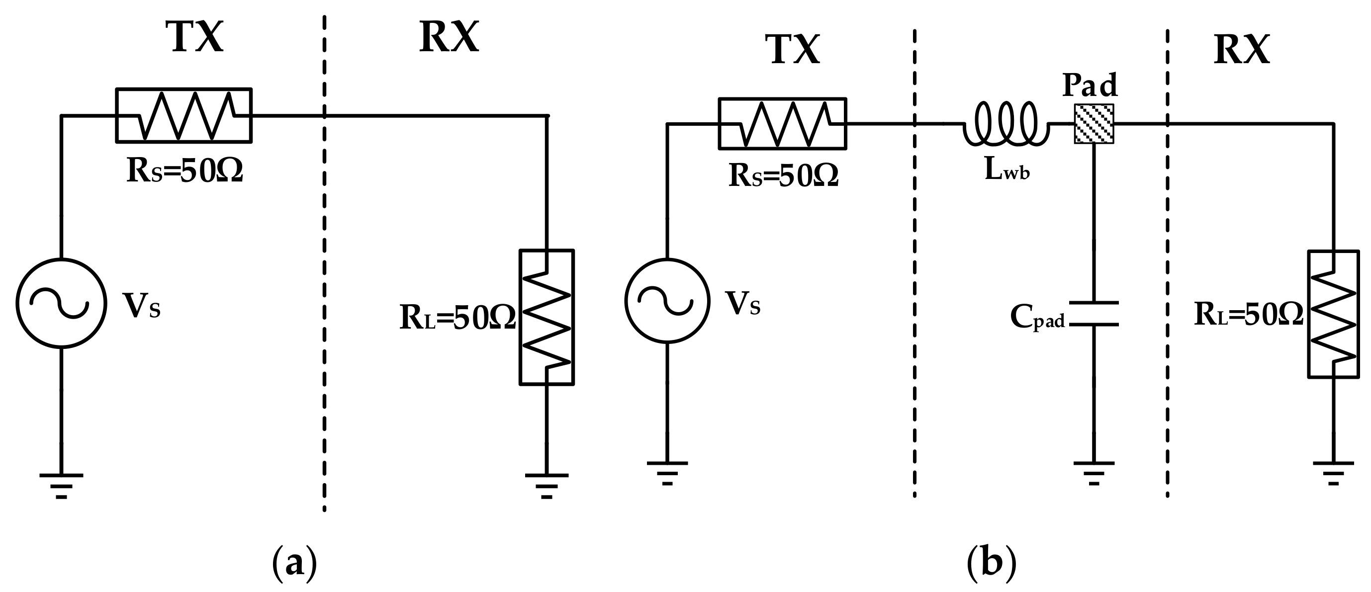
Figure 3a, the common way to receive the input signal source is through a 50 Ω matching resistor. However, in the practical chip design, there are some non-ideal factors that cause attenuation of the high-frequency signal. When the chip is packaged, the pins of the chip and the pins of the package are connected together by bonding wire to achieve the purpose of electrical connection. The bonding wire is generally long, so it will introduce a large equivalent inductor. On the other hand, the pin of the chip is a metal pad with a large area, which has a large parasitic capacitance to ground on the layout. Considering these two non-ideal factors, the equivalent circuit is shown in Figure 3b. Lwb is the equivalent inductor of the bonding wire between the chip pad and the package pin, and Cpad is the parasitic capacitor from the pad to ground. This circuit shows a low-pass filter feature. When the high-frequency signal is input, the non-ideal parasitic will cause attenuation that reduces the bandwidth of the analog input signal.
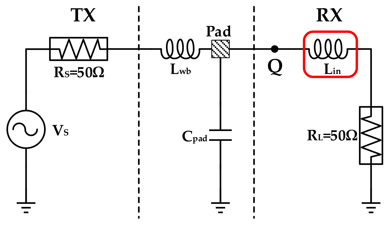
In order to solve the signal attenuation caused by this non-ideal factor and increase the analog bandwidth, the wideband front-end matching circuit is used in this design, as shown in Figure 4. Before the load resistance RL, an on-chip inductor Lin is implemented in series. Through reasonable parameter design, the resonant circuit shows the characteristics of high-pass filter and increases the bandwidth [18,19].
At this time, the load impedance seen from the signal source is:
Z ( ω ) = j ω L w b + 1 j ω C p a d + 1 j ω L i n + R L + R s
The voltage at point Q is:
V Q ( ω ) = V s | Z ( ω ) | | 1 1 R L + j ω L i n + j ω C p a d |
According to Equation (2), the voltage-frequency characteristics of the point Q varying with the input signal frequency can be obtained, as shown in Figure 5.
It can be seen from Figure 5 that there is one resonance frequency point in the voltage -frequency curve. The voltage of the point Q increases with the increase of the input frequency and reaches the maximum value when the frequency reaches f1. After that, the voltage decays quickly. According to this characteristic, the frequency point f1 can be set to the highest frequency of the input signal according to adjust the size of Lin. Then when a high-frequency signal is input, the amplitude of the signal received by the load increase, which can achieve the effect of amplifying the high-frequency signal and increasing the analog input bandwidth of the circuit. Compared with other complex designs, this wideband front-end matching circuit can effectively expand the bandwidth with a small cost.

3.2. Novel Calibration of Comparator Offset

Sub-ADC uses the flash structure to achieve the fast single-channel conversion rate. As a core module of the flash ADC, the comparator plays a key role in signal quantization. It quantizes the input analog signal to a digital code of 0 or 1. The speed and accuracy of the quantization directly determine the overall performance of the ADC. For the high-speed comparator, its offset is easily affected by non-ideal factors such as asymmetry of layout and process mismatch. The offset voltage of comparator can be seen equivalently as an excursion in the conversion curve, which causes an error in the conversion result.
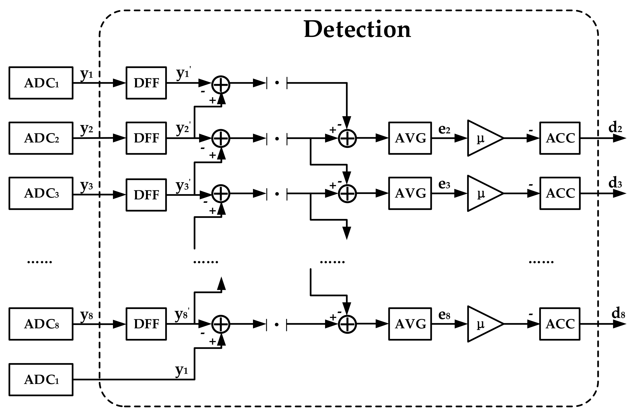
For the comparator offset in the flash ADC, a novel offset calibration is proposed in this paper, as shown in the Figure 6. Generally, the calibration is composed of detection and correction. A statistics-based offset detection is proposed to implement the offset detection. There are fifteen comparators with different thresholds in the comparator array, and each of them needed to be calibrated. The proposed detection works as follows. First of all, the offset detection of the comparator whose threshold voltage is the middle value among comparators is performed. Ideally, if a statistically symmetrical signal is input, such as a sine wave, the ratio of 0 and 1 output from this comparator should be approximately equal. Based on the above conclusion, the output distribution of the middle comparator is counted when a symmetrical distribution signal is input within a certain sampling point. If the ratio of 1 is greater/less than the ratio of 0, then the threshold of this comparator is adjusted to low/high direction through the offset correction circuit. The convergent iteration process based on least mean square (LMS) algorithm is performed as follows:
D c a l [ i + 1 ] = D c a l [ i ] + s i g n ( C d ) μ
where Dcal[i + 1] is (i + 1)th digital detection code of offset calibration, Dcal[i] is ith digital detection code of offset calibration, Cd is the result of comparing 1 and 0 numbers, μ is the convergence step factor. If μ is a constant value, the fixed step will make the convergence time proportional to offset. The larger comparator offset occurs, the more time it will take to accomplish the convergence. Figure 7a shows the simulated calibration convergence with fixed step. For this situation, a dynamic step adjustment method is implemented in the proposed detection. The convergence step is no longer a fixed value, but a dynamic value related to the ratio of 0 and 1. Figure 7b shows the simulated calibration convergence with the proposed dynamic step. It is obvious that convergence speed with the proposed dynamic step is faster than fixed step.
After a number of loop iterations, the offset calibration value of the comparator can converge to a suitable value. At this time, the ratio of 0 and 1 output by the comparator is approximately equal, which indicates the offset calibration of this comparator is over.
For the offset detection of other comparators, a comparator threshold reference voltage adjustment circuit is designed on chip. According to the distribution of the comparator threshold, the threshold reference voltage of other comparators can be adjusted to the threshold of the middle comparator one by one, and then perform the offset detection according the above detection method until offset detection of 15 comparators is completed.
For dynamic comparators, the common offset correction methods are as follows [20,21]. Adding an adjustable capacitor at the output of the comparator is one way to calibrate the offset. By adjusting the size of the capacitors at both ends, the discharge speed at both ends of the circuit can be the same, thereby eliminating the offset. But this method will increase the load of circuit and reduce the conversion speed of the comparator. Another way is to draw out the substrate of the differential input MOSFETs, and change the threshold voltage of them by adjusting the substrate voltage to narrow the input offset. This method will not affect the normal operation of the circuit, but the special deep well devices need to be used to separate the substrate of the NMOSFET in the CMOS process. There is also a method of adding a pair of auxiliary differential pairs. By adjusting the gate voltages of the calibrated differential MOSFETs, the offset of the circuit itself is cancelled. The disadvantage of this method is that it will increase the noise of the comparator.
The schematic diagram of two-stage dynamic comparator is shown in Figure 8. The first-stage pre-amplifier before the dynamic comparator can isolate the reset signal from the input signal, thereby greatly reducing the noise fed back by the comparator to the input. Another function of the pre-amplifier is to convert the input common-mode voltage to an appropriate range to increase the regeneration speed of the second-stage dynamic comparator. The positive feedback of the second-stage comparator can output a comparison result and ensure the speed of the comparator.
For the comparator offset, we propose a method to correct the comparator offset by adjusting the bias current of pre-amplifier. In the pre-amplifier, a current mirror structure is generally used to provide a gate bias to the PMOS transistor load, and the equivalent load of the PMOS transistor can be changed by adjusting the magnitude of the bias current to calibrate the comparator offset. The PMOS transistor load at the right end of the pre-amplifier in Figure 8 is connected to the fixed bias current Ibias, and the load at the left end is connected to the adjustable bias current Ical. Assuming that the input offset voltage of the comparator is Voffset, the voltage difference generated at the output of the pre-amplifier is:
V o u t , o f f s e t = g m 1 , 2 R 0 V o f f s e t
Among them, R0 is the output resistance of the pre-amplifier, and gM1,2 is the transconductance of the transistor M1, M2. The M1 and M2 are thin-oxide devices that can meet the speed requirement of the comparator. In order to calibrate the output voltage difference, the calibration current Ical needs to be adjusted as:
Δ I c a l = V o u t , o f f s e t K R 0 = g M 1 , 2 V o f f s e t K
In the Equation (5), K is the multiple of the current mirror. This offset correction method will neither increase the load on the intermediate nodes of the circuit nor affect the normal working sequence of the circuit. It does not affect the speed of the comparator, so it is suitable to use it in high-speed circuits.
The correction current Ical is generated by the current-steering DAC, which is controlled by the offset detection output code. Ideally, the weight of the 7-bit input code of the current-steering DAC is 1, 2, 4, 8, 16, 32, 64 (set the minimum transition value of the current-steering DAC output as 1 LSB). But in fact, due to factors such as process and layout, the equivalent weight will drift. If the circuit corresponding to the 32-weighted input code is affected by the process mismatch and its equivalent weight drifts to 36, then the codes of 33/34/35 LSB will disappear. Figure 9a shows the transmission curve of non-ideal 7-bit DAC in this case. If the ideal offset calibration convergence value is 34 LSB, DAC output will jump between 32 LSB and 36 LSB eventually, as shown in Figure 10a. This will affect the accuracy of the calibration.
In order to achieve an accurate offset correction, the mismatch-insensitive offset correction is proposed. A 7-bit precision correction is taken as the example.
First of all, an 8-bit DAC with a redundant bit is designed based on the original 7-bit current-steering DAC in analog domain. The redundant bit weight is set as 8 LSB to cover mismatches less than 8 LSB. The ideal bit-weights of the 8-bit current-steering DAC are 1, 2, 4, 8, 8, 16, 32 and 64 now.
Second, the redundant encoder module is integrated to expands the 7-bit Dcal(n) into 8-bit DR,cal(n) in digital domain. It works in four steps:
  • The full-scale of the 7-bit digital control code is divided into 16 intervals of length 8
  • Judge the slope of the interval code of Dcal(n)
  • Determine whether to use the two 8 weighted bits to replace the 16 weighted bit according to the slope of Dcal(n)
  • Obtain the 8-bit DR,cal(n) with a redundant bit.
The conversion characteristic of non-ideal 8-bit redundant current-steering DAC is shown in the Figure 9b. With the help of this algorithm, the redundant current-steering DAC output can be adjusted according to the slope of offset detection output code. Figure 10b shows the simulation of the calibration convergence with non-ideal 8-bit redundant current-steering DAC based on proposed algorithm. It is obviously that the convergence eventually reaches 34 LSB when the end point of the offset calibration convergence value is 34 LSB.
The proposed offset calibration algorithm can achieve quick detection and accurate correction with low cost. Meanwhile, it does not affect the speed of the comparator, so it is suitable to use it in high-speed circuits.

3.3. Multi-Phase High-Speed Clock Generation and Calibration

Time-interleaved ADC requires multi-phase clock signals to drive each sub-ADC to work normally. Usually, the chip only inputs a main clock signal, and the clock generation circuit needs to generate multi-phase signals to drive the sub-ADCs to work normally. The sampling rate of the chip in this design is 36 GS/s, and the frequency of the main clock signal generated by the chip’s own PLL is 18 GHz. According to the working timing of the interleaved ADC in Figure 1b, the clocks required for each channel are 4.5 GHz clock signals. Therefore, it is necessary to divide the 18 GHz main clock into 4.5 GHz multi-phase clock to drive the multi-channel to work orderly.
The CMOS clock divider circuit has a simple structure and no static power consumption, but the speed is slow, which is suitable for low-frequency clock processing; the CML clock divider circuit works fast, but the power consumption and area consumption are large [22,23]. Based on comprise between speed and power consumption, a multi-phase high-speed clock generation circuit based on CMOS and CML is presented in this design. The CML clock divider circuit is used to divide the high-frequency clock signal in the first stage to ensure the quality of the high-frequency output clock. After the frequency division, the frequency of output clock is halved. Then use the CMOS clock divider circuit to divide the clock in the second stage to reduce the power consumption of the overall circuit. Figure 11a is a schematic diagram of the first-stage CML frequency-dividing circuit, which divides the differential master clock into 4 different-phase 9 GHz clock signals CLK_4<1:4>; Figure 11b is a schematic diagram of the second-stage frequency-dividing circuit, which divide the 4 different-phase 9 GHz clock signals into 8 different-phase 4.5 GHz clock signals CLK_8<1:8>. The voltage waveform of each node in the circuit is shown in Figure 11c.
CLK_8<1:8> is a 4.5 GHz clock signal with a 50% duty cycle, which is used as the clock drive signal for the comparator array of each channel. For the sample-and-hold circuit of the ADC, a 4.5 GHz clock signal with a duty cycle of 25% is required. These signals can be generated by simple combinational logic between CLK_8<1:8> and CLK_4<1:4>. As shown in the Figure 12, the logical operation of C4<2> and C8<1> and C8<5> signals respectively can obtain 4.5 GHz clock signals C1 and C5 with a duty ratio of 25%, which drives the track-and-hold circuit of each channel to work normally. The Figure 12 only shows the processing of the clock signals in two phases, and the clock generation methods of the other phases are the same. The proposed clock divider circuit guarantees the working speed without causing large power consumption.
The 8 different-phase clock signals generated by the above scheme are used to drive the eight time-interleaved sub-ADCs. Ideally, the phase difference between adjacent phase clock signals should be 45°. However, the incomplete symmetry of the circuit on the layout will cause the route length of the multiphase clock signal to be different, which will bring mismatch to the delay of the multi-phase clocks. On the other hand, the process mismatch in chip production will also cause timing mismatch. These will make the delay of the output clock of the frequency dividing circuit reach each channel different. The timing mismatch among the channels will reduce the overall linearity of the time-interleaved ADC [24,25].
In order to solve this problem, a timing mismatch calibration module is integrated to achieve the timing mismatch detection and correction [12]. Using high-speed finite impulse response (FIR) filters is a way to correct the timing mismatch in digital domain, but it is complex and the power consumption is large [26,27]. VDL is a simple and effective way to achieve the timing mismatch correction in analog domain, but the timing mismatch detection is not easy to realize. A wideband timing mismatch detection (WTD) is proposed and utilized on chip, as shown in Figure 13.
Now suppose that there are timing mismatches among sub-ADCs, the digital output codes from channel m (1 ≤ m ≤ 8) are
y m ( k ) = x [ ( 8 k + m ) T s + τ m ] G
where τm is the additional phase of each channel m due to timing mismatch. Channel 1 is used as a reference, so τ1 can be regarded as 0.
The τm can be extracted from the timing mismatch error em written as following:
e m = E [ | y m + 1 ( k ) y m ( k ) | | y m ( k ) y m 1 ( k ) | ] , 2 m 7 e 8 = E [ | y 1 ( k + 1 ) y 8 ( k ) | | y 8 ( k ) y 7 ( k ) | ]
It is difficult to prove the relationship between em and τm directly. But if the absolute value operation can be approximated by the squaring function, some conclusions can be derived [12]. Now, em can be simplified to:
e m E [ 2 y m + 1 ( k ) y m ( k ) ] E [ 2 y m ( k ) y m 1 ( k ) ] , 2 m 7
Substituting the Equation (6) into the Equations (8) and (9) can be obtained.
e m 2 G 2 [ R x ( T s + τ m τ m 1 ) R x ( T s + τ m + 1 τ m ) ] , 2 m 7
Because the timing mismatch is a very small amount relative to Ts, Equation (9) can be approximated to Equation (10):
e m 2 G 2 [ R x ( T s ) ( 2 τ m τ m + 1 τ m 1 ) ] , 2 m 7
Timing mismatch error of channel 8 is
e 8 2 G 2 [ R x ( T s ) ( 2 τ 8 τ 1 τ 7 ) ]
Among them, the derivative of autocorrelation Rx(t) can be expressed as
R x ( t ) = + j 2 π f S x ( f ) e j 2 π f t d f = 2 π + f [ j c o s ( 2 π f t ) s i n ( 2 π f t ) ] S x ( f ) d f
where Sx(f) denotes the signal spectrum. Since Sx(f) is an even function concerning f, it is easy to get the Equation (13):
R x ( t ) = 4 π 0 + f s i n ( 2 π f t ) S x ( f ) d f
If the input signal x(t) is bandlimited to the Nyquist frequency, Rx′(Ts) can be expressed as Equation (14) based on the mean value theorem of integrals.
R x ( T s ) = 4 π ξ s i n ( 2 π ξ T s ) 0 1 / ( 2 T s ) S x ( f ) d f , ξ ( 0 , 1 / ( 2 T s ) )
Because the item −4πζsin(2πζTs) is a negative value and the integral of Sx(f) is positive, we can get the conclusion that Rx′(Ts) < 0. It indicates that the sign of 2τmτ(m+1)modMτm−1 and em are different if there is a timing mismatch among them. em can be subtracted cumulatively and feedback the result to the timing mismatch correction until em turns to zero, which indicates the completion of detection.
Compared with algorithm proposed in [12], the WTD can achieve the timing mismatch detection of all channels at the same time. This saves time waiting for the completion of intermediate channel calibration before calibrating other channels. So the proposed algorithm can achieve fast timing mismatch detection as long as the input signal is bandlimited to the Nyquist frequency for the complete ADC system.

4. Measurement Results

The ADC occupies an area of 2.96 mm × 1.8 mm in a 40 nm CMOS process. Figure 14 shows its micrograph, including eight sub-ADCs, PLL, digital module and serializers output. In order to keep the power supply voltage clean and stable, a large number of decoupling capacitors are filled in the spaces between different modules.
Figure 15 shows the static performance of the differential nonlinearity (DNL) and integral nonlinearity (INL). The measured DNL and INL before the TI mismatch calibration and offset calibration are −0.77/+0.96 and −0.76/+0.76 respectively. After the calibration, they are improved to −0.28/+0.22 LSB and −0.19/+0.16 LSB, as shown in Figure 16.
The output spectrums before and after calibration can indicate the effect of calibration the. Before the error between the channels and the offset of each comparator are calibrated, the spectrum characteristics of the ADC output when the proposed ADC worked at a sampling rate of 36 GS/s and input a 1.2 GHz sinusoidal signal are shown in Figure 17a. It can be seen that in addition to the high-order harmonic components of the signal, there are also spurs caused by offset, gain and timing mismatch. The spurs generated by the offset mismatch appear at the frequency of k*fs/8. The spurs produced by the mismatch of the gain and timing appear at the frequency of k*fs/8 ± fin. At the same time, because the offset of the sub-ADC comparator array is not calibrated, there are many other spurs in the spectrum. The SNDR of the output signal is 13.05 dB and the SFDR is 20.83 dB before calibration. After calibrating the mismatch between the channels of the chip and the offset of each comparator, the output spectrum when the sampling rate is 36 GS/s and the input frequency is 1.2 GHz is shown in Figure 17b. It can be seen that the spurs generated by the mismatch between the channels and some harmonics are greatly reduced. The SNDR of the output signal is 22.57 dB and the SFDR is 35.71 dB.
When the input signal frequency is 8.1 GHz, the frequency spectrum is shown in Figure 18a. The SNDR of the output signal is 21.24 dB and the SFDR is 29.12 dB. When the input frequency is 17.1 GHz, the frequency spectrum is shown in Figure 18b. The SNDR of the output signal obtained from measurement is 18.6 dB, and the SFDR is 24.50 dB. The spurs produced by the mismatch of the gain and timing mismatch become the main spurious components. The higher the input frequency, the greater the impact of the timing mismatch on the output linearity.
Figure 19 shows the ADC performance with calibration versus the input frequency at 36 GS/s. It can be seen that in the input frequency range of 0~18 GHz, the SNDR of the ADC is greater than 18.6 dB, and the SFDR is greater than 24.5 dB. The ADC core consumes 780 mW powered at 0.9/1.2/1.8 V and the Walden figure of merit (FOM) of 1.9 pJ/step is achieved.
Table 1 summarizes the comparison of our results with previous published papers for ADCs. Our work achieves a relatively good SFDR with the help of the proposed calibration. Compared to the ADCs manufactured in SiGe process, the proposed ADC manufactured in CMOS process has lower power consumption and achieves a nice FOM.

5. Conclusions

A 4-bit 36 GS/s analog-to-digital converter (ADC) employing eight flash sub-ADCs with calibration is presented in this paper. A wideband front-end matching circuit based on a peaking inductor is designed to increase the analog input bandwidth to 18 GHz. A novel offset calibration that can achieve fast detection and accurate correction without affecting the speed of the comparator is proposed, guaranteeing the high-speed operation of the ADC. In order to balance speed, quality and power of the high-speed clock, a clock distribution circuit based on CMOS and CML is implemented in the proposed ADC. A timing mismatch calibration is also integrated into the chip, which can achieve the timing mismatch detection of the input signal that is bandlimited to the Nyquist frequency. The measurement results show that the proposed ADC can achieve an analog bandwidth of 18 GHz at the sampling rate of 36 GS/s. The DNL and INL are −0.28/+0.22 LSB and −0.19/+0.16 LSB, respectively. The SNDR is above 22.5 dB and SFDR is better than 35 dB at 1.2 GHz. It can achieve an SFDR above 24.5 dB and an SNDR above 18.6 dB across the entire Nyquist frequency. With a die size of 2.96 mm *1.8 mm, the ADC consumes 780 mW from the 0.9/1.2/1.8 V power supply. The calculated Walden figure of merit reaches 1.9 pJ/step.

Author Contributions

H.J. designed the circuits, analyzed the measurement data, and wrote the manuscript. X.G., X.Z., X.X., D.W., and L.Z. assisted the circuit simulation and implementation. X.G., X.Z. and J.W. guided the design, reviewed the manuscript and gave suggestions for revision; X.L. gave some valuable guidance and confirmed the final version of manuscript. All authors have read and agreed to the published version of the manuscript.

Funding

This research was funded by the Chinese Academy of Sciences Strategic Leading Science and Technology Project (Grant No. XDC07020100).

Conflicts of Interest

The authors declare no conflict of interest.

References

  1. Shannon, C.E. A mathematical theory of communication. Bell Syst. Tech. J. 1948, 27, 623–656. [Google Scholar] [CrossRef]
  2. Aiello, G.R.; Rogerson, G.D. Ultra-wideband wireless systems. IEEE Microw. Mag. 2003, 4, 36–47. [Google Scholar] [CrossRef]
  3. Chan, V.W.S. Optical space communications. IEEE J. Sel. Top. Quantum Electron. 2000, 6, 959–975. [Google Scholar] [CrossRef]
  4. Federici, J.; Moeller, L. Review of terahertz and subterahertz wireless communications. J. Appl. Phys. 2010, 107. [Google Scholar] [CrossRef] [Green Version]
  5. Walden, R.H. Analog-to-digital converter survey and analysis. IEEE J. Sel. Areas Commun. 1999, 17, 539–550. [Google Scholar] [CrossRef] [Green Version]
  6. Tang, J.; Xu, Z.; Sadler, B.M. Performance analysis of b-bit digital receivers for TR-UWB systems with inter-pulse interference. IEEE Trans. Wirel. Commun. 2007, 6, 494–505. [Google Scholar] [CrossRef] [Green Version]
  7. Hoyos, S.; Sadler, B.M.; Arce, G.R. Monobit digital receivers for ultrawideband communications. IEEE Trans. Wirel. Commun. 2005, 4, 1337–1344. [Google Scholar] [CrossRef]
  8. Ali, A.; Hamouda, W. A novel one-bit quantization design for correlation-based low-power wideband sensing. In Proceedings of the 2016 IEEE International Conference on Communications (ICC), Kuala Lumpur, Malaysia, 23–27 May 2016. [Google Scholar] [CrossRef]
  9. Zhang, Z.; Cai, X.; Li, C.; Zhong, C.; Dai, H. One-bit quantized massive MIMO detection based on variational approximate message passing. IEEE Trans. Signal Process. 2018, 66, 2358–2373. [Google Scholar] [CrossRef]
  10. Kertis, R.A.; Humble, J.S.; Daun-Lindberg, M.A.; Philpott, R.A.; Fritz, K.E.; Schwab, D.J.; Prairie, J.F.; Gilbert, B.K.; Daniel, E.S. A 20 GS/s 5-Bit SiGe BiCMOS dual-nyquist flash ADC with sampling capability up to 35 GS/s featuring offset corrected exclusive-or comparators. IEEE J. Solid State Circuits 2009, 44, 2295–2311. [Google Scholar] [CrossRef]
  11. Limotyrakis, S.; Kulchycki, S.D.; Su, D.K.; Wooley, B.A. A 150-MS/s 8-b 71-mW CMOS time-interleaved ADC. IEEE J. Solid State Circuits 2005, 40, 1057–1066. [Google Scholar] [CrossRef]
  12. Wei, H.; Zhang, P.; Sahoo, B.D.; Razavi, B. An 8 Bit 4 GS/s 120 mW CMOS ADC. IEEE J. Solid State Circuits 2014, 49, 1751–1761. [Google Scholar] [CrossRef]
  13. Black, W.C.; Hodges, D.A. Time interleaved converter arrays. IEEE J. Solid State Circuits 1980, 15, 1022–1029. [Google Scholar] [CrossRef]
  14. Tretter, G.; Khafaji, M.M.; Fritsche, D.; Carta, C.; Ellinger, F. Design and characterization of a 3-bit 24-GS/s flash ADC in 28-nm low-power digital CMOS. IEEE Trans. Microw. Theory Tech. 2016, 64, 1143–1152. [Google Scholar] [CrossRef]
  15. Feng, Y.; Tang, Y.; Fan, Q.; Chen, J. A 25-GS/s 4-bit single-core flash ADC in 28 nm FDSOI CMOS. In Proceedings of the 2018 IEEE Asia Pacific Conference on Circuits and Systems (APCCAS), Chengdu, China, 26–30 October 2018; pp. 30–33. [Google Scholar] [CrossRef]
  16. Joonsuk, L.; Beomsup, K. A low-noise fast-lock phase-locked loop with adaptive bandwidth control. IEEE J. Solid State Circuits 2000, 35, 1137–1145. [Google Scholar] [CrossRef]
  17. Hsieh, G.-C.; Hung, J.C. Phase-locked loop techniques. A survey. IEEE Trans. Ind. Electron. 1996, 43, 609–615. [Google Scholar] [CrossRef]
  18. Ohkawa, N. Fiber-optic multigigabit GaAs MIC front-end circuit with inductor peaking. J. Light. Technol. 1988, 6, 1665–1671. [Google Scholar] [CrossRef]
  19. Poulton, K.; Neff, R.; Setterberg, B.; Wuppermann, B.; Kopley, T.; Jewett, R.; Pernillo, J.; Tan, C.; Montijo, A. A 20GS/s 8b ADC with a 1MB memory in 0.18μm CMOS. In Proceedings of the 2003 IEEE International Solid-State Circuits Conference, Digest of Technical Papers, ISSCC., San Francisco, CA, USA, 13 February 2003; pp. 318–496. [Google Scholar] [CrossRef]
  20. Miyahara, M.; Asada, Y.; Paik, D.; Matsuzawa, A. A low-noise self-calibrating dynamic comparator for high-speed ADCs. In Proceedings of the 2008 IEEE Asian Solid-State Circuits Conference, Fukuoka, Japan, 3–5 November 2008; pp. 269–272. [Google Scholar] [CrossRef]
  21. Wong, Y.L.; Cohen, M.H.; Abshire, P.A. A 1.2-GHz comparator with adaptable offset in 0.35-μm CMOS. IEEE Trans. Circuits Syst. I Regul. Pap. 2008, 55, 2584–2594. [Google Scholar] [CrossRef]
  22. Allam, M.W.; Elmasry, M.I. Dynamic current mode logic (DyCML): A new low-power high-performance logic style. IEEE J. Solid State Circuits 2001, 36, 550–558. [Google Scholar] [CrossRef]
  23. Allstot, D.J.; Liang, G.; Yang, H.C. Current-mode logic techniques for CMOS mixed-mode ASICs. In Proceedings of the IEEE 1991 Custom Integrated Circuits Conference, San Diego, CA, USA, 12–15 May 1991; Volume 2, pp. 25.2/1–25.2/4. [Google Scholar]
  24. Law, C.H.; Hurst, P.J.; Lewis, S.H. A four-channel time-interleaved ADC with digital calibration of interchannel timing and memory errors. IEEE J. Solid State Circuits 2010, 45, 2091–2103. [Google Scholar] [CrossRef]
  25. Mafi, H.; Yargholi, M.; Yavari, M. Digital blind background calibration of imperfections in time-interleaved ADCs. IEEE Trans. Circuits Syst. I Regul. Pap. 2017, 64, 1504–1514. [Google Scholar] [CrossRef]
  26. Schmidt, C.A.; Cousseau, J.E.; Figueroa, J.L.; Reyes, B.T.; Hueda, M.R. Efficient estimation and correction of mismatch errors in time-interleaved ADCs. IEEE Trans. Instrum. Meas. 2016, 65, 243–254. [Google Scholar] [CrossRef]
  27. Liu, S.; Li, Z.; Zhao, Z.; Fan, Y. All-digital background calibration technique of the channel-time-mismatch in a two-channel TIADC. In Proceedings of the 2017 IEEE 12th International Conference on ASIC (ASICON), Guiyang, China, 25–28 October 2017; pp. 632–635. [Google Scholar] [CrossRef]
  28. Li, J.; Chen, Y.; Tang, P.; Zhang, Z.; Wang, H.; Huang, H. A low-power low-distortion 20-GS/s flash analog-to-digital converter for coherent optical receiver in 0.13-μ m SiGe BiCMOS. J. Circuits Syst. Comput. 2019, 28. [Google Scholar] [CrossRef]
  29. Ritter, P.; Le Tual, S.; Allard, B.; Möller, M. Design considerations for a 6 bit 20 GS/s SiGe BiCMOS flash ADC without track-and-hold. IEEE J. Solid State Circuits 2014, 49, 1886–1894. [Google Scholar] [CrossRef]
  30. Du, X.Q.; Grozing, M.; Buck, M.; Berroth, M. A 40 GS/s 4 bit SiGe BiCMOS flash ADC. In Proceedings of the 2017 IEEE Bipolar/BiCMOS Circuits and Technology Meeting (BCTM), Miami, FL, USA, 19–21 October 2017; pp. 138–141. [Google Scholar] [CrossRef]
Figure 1. (a) Overall architecture and (b) overall timing diagram of the proposed ADC.
Electronics 09 01733 g001
Figure 2. Block diagram of the single-channel ADC.
Electronics 09 01733 g002
Figure 3. Input matching circuit (a) ideal and (b) non-ideal.
Electronics 09 01733 g003
Figure 4. The proposed input matching circuit.
Electronics 09 01733 g004
Figure 5. Voltage-frequency characteristics of the point Q.
Electronics 09 01733 g005
Figure 6. Overall block diagram of the proposed statistics-based offset detection.
Electronics 09 01733 g006
Figure 7. Simulated calibration convergence with (a) fixed step and (b) the proposed dynamic step.
Electronics 09 01733 g007
Figure 8. Schematic diagram of two-stage dynamic comparator.
Electronics 09 01733 g008
Figure 9. The conversion characteristic of (a) non-ideal 7-bit DAC and (b) 8-bit DAC based on proposed algorithm.
Electronics 09 01733 g009
Figure 10. Simulated the calibration convergence of (a) non-ideal 7-bit current-steering DAC and (b) non-ideal 8-bit redundant current-steering DAC based on proposed algorithm.
Electronics 09 01733 g010
Figure 11. (a) The schematic diagram of the CML frequency-dividing circuit, (b) the second-stage frequency-dividing circuit and (c) voltage waveform of each node in the frequency-dividing circuit.
Electronics 09 01733 g011
Figure 12. 25% duty cycle clock signal generation and voltage waveform.
Electronics 09 01733 g012
Figure 13. Overall block diagram of wide band timing-mismatch detection.
Electronics 09 01733 g013
Figure 14. The micrograph of prototype ADC.
Electronics 09 01733 g014
Figure 15. Measured (a) INL and (b) DNL performance before calibration.
Electronics 09 01733 g015
Figure 16. Measured (a) INL and (b) DNL performance after calibration.
Electronics 09 01733 g016
Figure 17. Measured output spectrum when fin = 1.2 GHz (a) before calibration and (b) after calibration
Electronics 09 01733 g017
Figure 18. Measured output spectrum (a) when fin = 8.1 GHz and (b) when fin = 17.1 GHz.
Electronics 09 01733 g018
Figure 19. SNDR/SFDR of the ADC versus frequency of the input signal at 36 GS/s.
Electronics 09 01733 g019
Table 1. Performance comparison with state-of-art ADCs.
Reference[14][28][29][30]This Work
Technology28 nm CMOS0.13 um SiGe0.13 um SiGe0.13 um SiGe40 nm CMOS
Sampling rate (GS/s)2420204036
Resolution (bits)34644
Supply (V)1.4/1.7544.5/3.33.5/30.9/1.2/1.8
SNDR (dB)@HF1515.524.318.618.6
SFDR (dB)@HF2220.826.52424.5
Power (mW)400180010002300780
FOM (pJ/step)3.610.73.98.31.9
Publisher’s Note: MDPI stays neutral with regard to jurisdictional claims in published maps and institutional affiliations.

