1. Introduction
Photovoltaic (PV) energy production has witnessed a steady increase in the past 15 years. The growth has been fueled by technological advancements and the support of incentive programs from the world’s governments. Nowadays, the scenario for power electronics is well-established [
1,
2], and several possibilities are present for different power levels, ranging from (Megawatt) MW -scale centralized inverters (for very large solar arrays), to the medium-power solution (single and three-phase) to the micro-inverter type, also called a string inverter or module-integrated converter (MIC). They are usually single-phase converters which are directly connected to the grid. This latter type has been in the spotlight due to its unique advantages, including:
Individual Maximum Power Point Tracking (MPPT) is possible, where this allows for better extraction efficiency, preventing the partial shading phenomena.
High availability of the system, since the failure of a power electronics module would minimally impact the performance of a bigger system.
Since the module would have an AC output, the installation and protection system would be cheaper, due to the absence of a high-voltage DC distribution, as in some centralized inverter solutions.
An initial classification of the MICs has been proposed in [
3]. One of the peculiar problems of the photovoltaic systems is the possibility of ground leakage current insurgence [
1], due to the parasitic capacitance between the photovoltaic cells and the ground and the electric distribution. The typical solutions imply a transformer (either high-frequency or low-frequency), but transformerless solutions normally feature better efficiency and lower weight. For years, the main topologies have been based on the Voltage Source Inverter paradigm, and modifications to the unidirectional full-bridge or to the three-phase bridge with additional switches were proposed to reduce the common mode voltage generation, which causes the ground leakage current [
4,
5,
6]. Recently, the Z-source or quasi-Z-source [
7] have been employed for MICs, due to the advantage of low ground leakage current and intrinsic boost capability.
This article critically analyses a modified Current Source Inverter topology, named CSI5, that is able to improve the performance of the basic single-phase CSI in terms of efficiency and is also capable of reducing the ground leakage current to almost zero. Recently, PV CSI architectures have been proposed for full-sized PV arrays, both in single-phase [
8,
9] and three-phase [
10] architectures, but also for MIC solutions for three-phase distribution grids [
11]. The CSI5 topology was proposed for the first time in [
12], where the present work further expands the theoretical and simulation analysis, offering a comprehensive coverage of the benefits and drawbacks of single-phase CSI for PV applications, and in particular of the proposed solution. These improvements are analyzed in the following sections in order to verify the effectiveness of this power converter employed as a PV MIC. The contribution of this paper is a thorough analysis of the CSI5 topology with active decoupling devices, which clamp the output of the H-bridge stage during the zero states of the pulse width modulation, allowing for extremely low levels of ground leakage current.
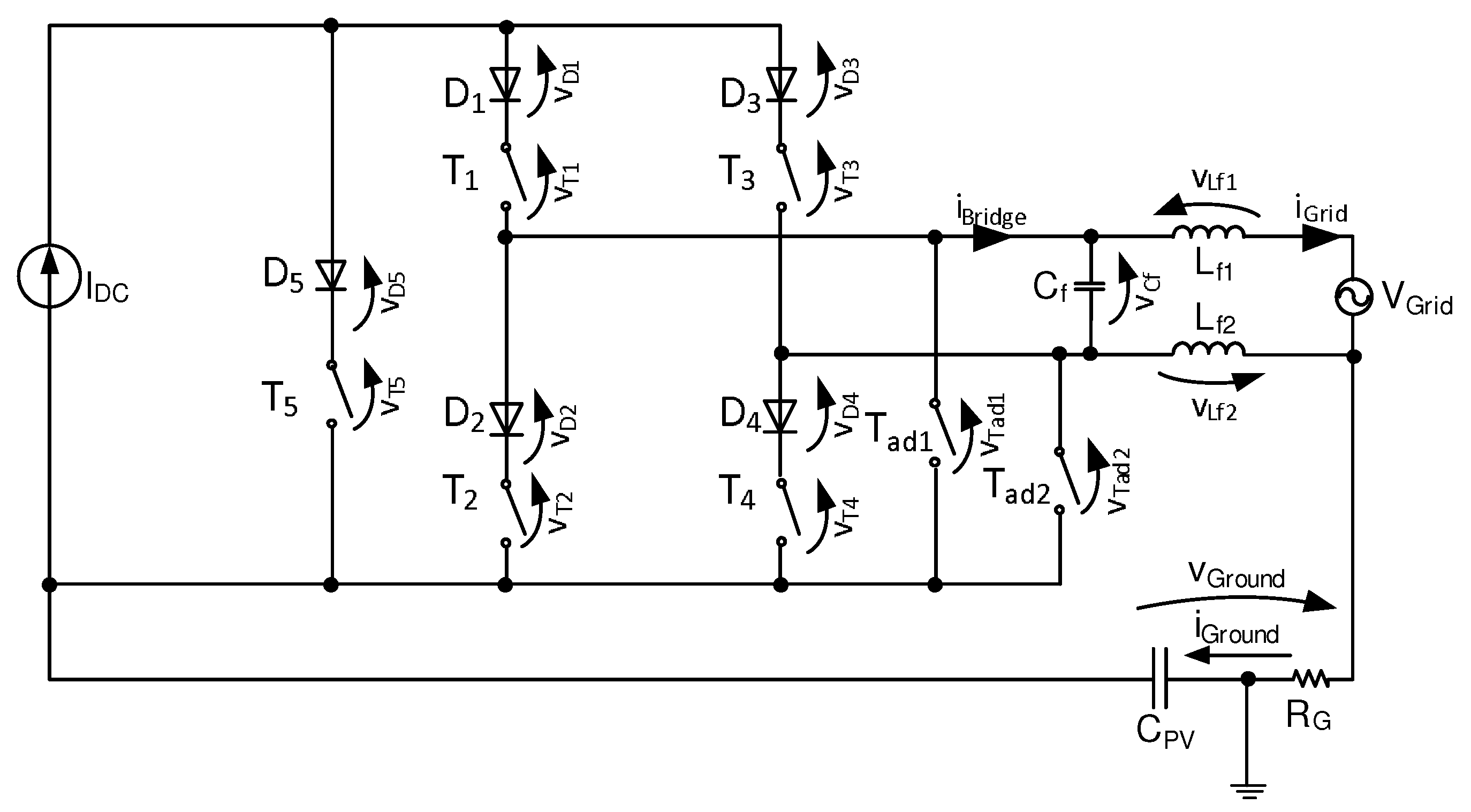
2. Basic Single-Phase CSI Topology
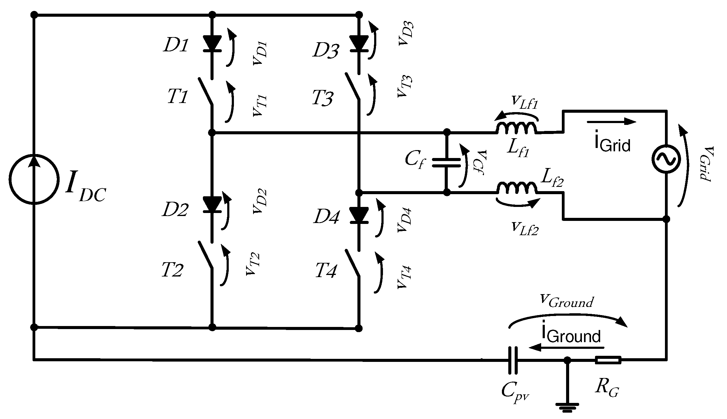
Figure 1 shows the basic single-phase Current Source Inverter (CSI) for a photovoltaic grid connected system: it is worth noticing that the schematic features the equivalent parasitic capacitance,
, of the PV string connected between the earth and the frame of the PV panels [
13]; resistance
represents the ground resistance between the neutral connection and the earth. For simplicity’s sake, only a lumped capacitor connected to the negative DC rail of the panels is considered, and it holds the overall capacitance of the panels. The capacitance connected to the positive rail of the panel (the panel not shown in
Figure 1) is not drawn, because the capacitance of both DC rails are connected in parallel in the equivalent common-mode circuit. Since for the PV converter, the main source of capacitance to the ground is the panel parasitic one, the capacitance of the devices to the heatsink and then to the ground are not considered for this work.
This topology, like all single-phase PV topologies, faces the drawback of matching a pulsating power to a constant power source. For the CSI, this is even more critical, since the energy would need to be stored in the DC inductor, which would imply unacceptable values in terms of weight and size.
This issue will be discussed later in the manuscript, and in this section the assumption of a constant DC current source will be made for the operating principle explanation.
2.1. CSI Operating Principle
The basic principle of the CSI is that a constant current source (for example, by employing an inductor) is modulated to synthesize an arbitrary current waveform at the output. To reduce distortion in the output current waveform, a filter comprising a capacitor, or a capacitor and an inductor, is placed to realize the coupling to the grid. In the case of a simple capacitive filter, the inductance of the grid would act as an inductive element to limit the high-frequency current harmonics injected into the grid. However, to prevent excessive voltage distortion at the point of common coupling (PCC), a physical inductor is preferred. The immediate advantages of this topology is the ease of current control (the current is directly controlled via the modulation index), the intrinsic voltage boost capabilities, the high reliability due to the low failure rate of the inductor if compared to an electrolytic capacitor, as well as the intrinsic short-circuit protection inherent of the topology.
On the other hand, the presence of two devices connected in series (the diode and the transistor) to realize a bi-directional voltage blocking device has a strong impact on the efficiency due to increased conduction losses, an aspect which has limited the widespread adoption of CSI topologies.
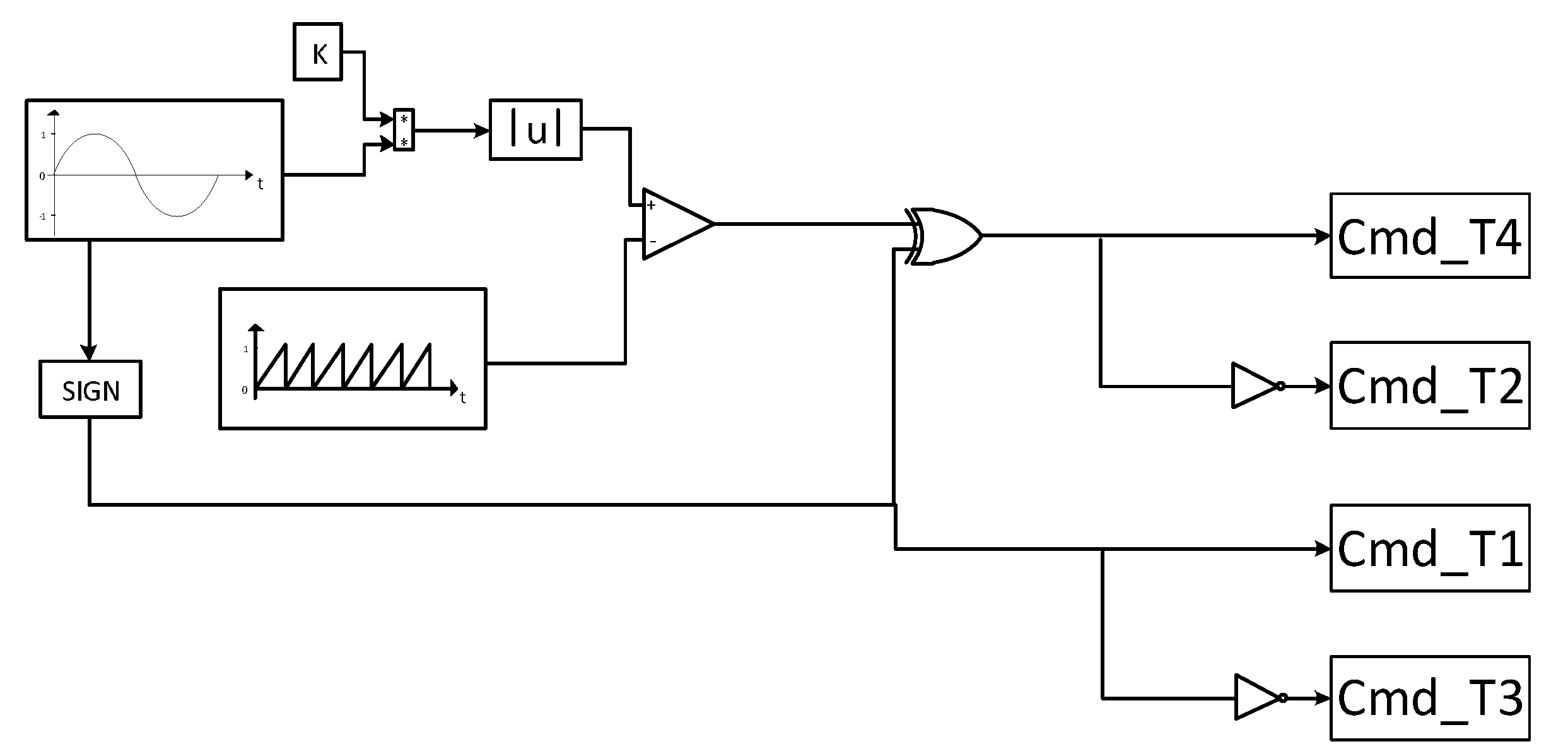
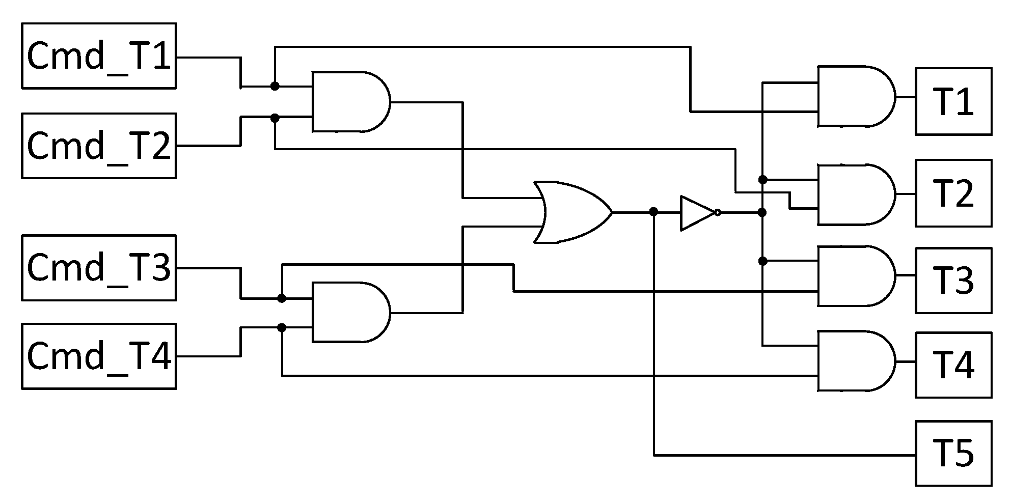
The command sequence of the four transistors in the unidirectional full-bridge (T1, T2, T3, and T4) is obtained with the strategy shown in
Figure 2. Considering grid-tied operation, the sinusoidal waveform shown in
Figure 2 represents the reference shape of the current, which can be extracted with a Phase-Locked Loop (PLL) or can be obtained from the grid voltage measurement.
The basic operation implies that for each grid-voltage half-wave, a diagonal of the H-bridge is switched on for a time, depending on the reference (active state), providing the DC-link current to the grid. During the remaining switching period, a shoot-through state (zero state) is applied to the H-bridge. In this latter case, zero current is provided to the grid [
12].
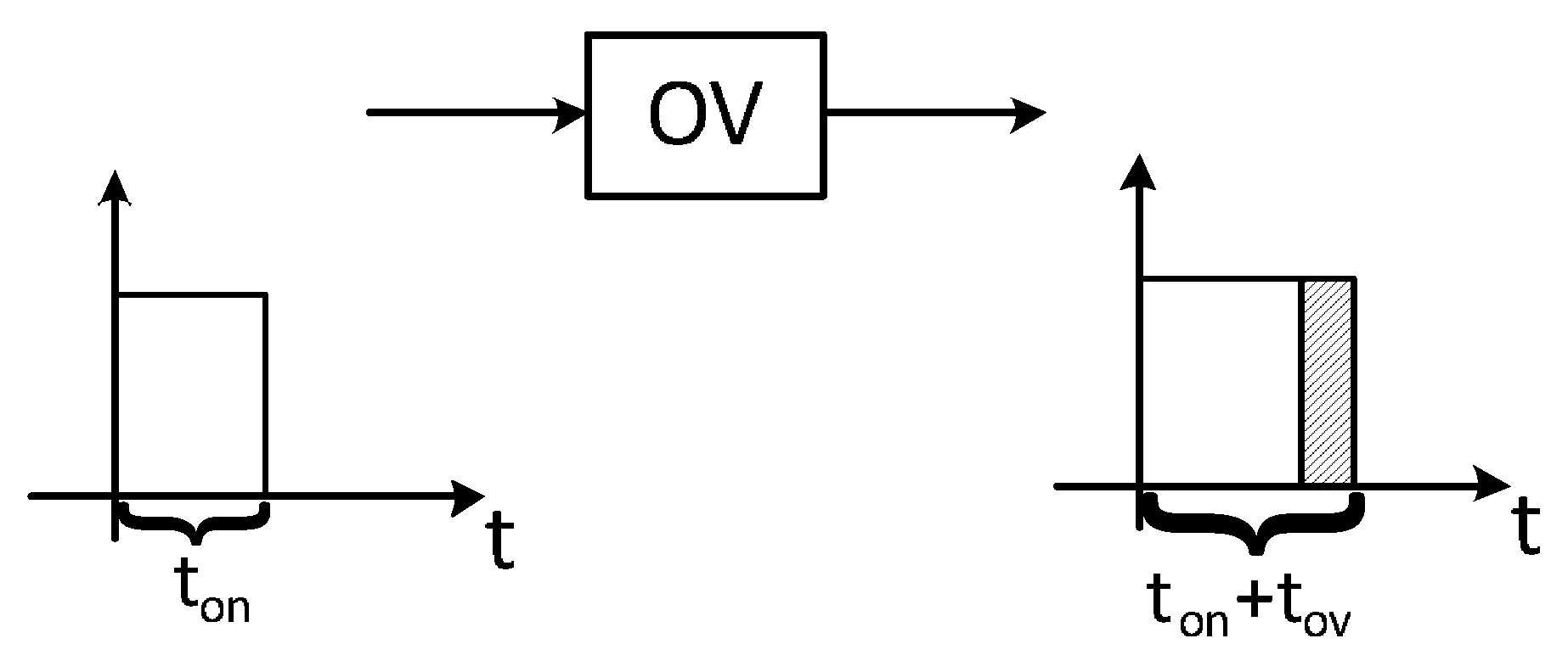
Similarly to the dead-time that is applied between the switches of a VSI, an overlap time is introduced in the commutation of the CSI to prevent the DC-link open-circuit, as shown in
Figure 3.
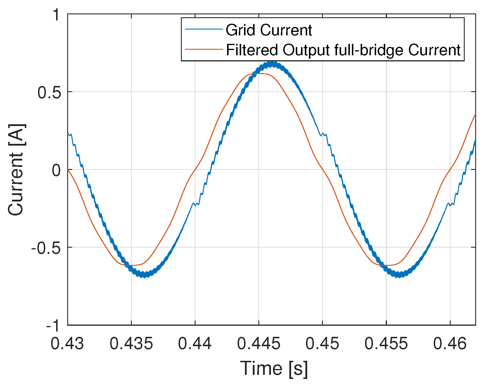
The result of the commutation process is shown in the exemplified condition of
Figure 4, where the grid current and a zero-phase filtered version [
14] of the bridge output current are shown. It can be seen that a small phase shift and amplitude difference exists, due to the current absorbed by the output filter. This effect can be compensated for by properly adjusting the reference to compensate for the current absorbed by the output C-L filter.
2.2. Common Mode Voltage Analysis for the CSI Topology
The theoretical tool used for the analysis of the ground leakage current in grid-connected Pulse Width Modulation (PWM) is usually the common mode voltage evaluation, as shown in the relevant literature for the VSI [
15,
16].
For the CSI application, due to the different operating principles, the analysis of the ground leakage current is performed with the evaluation of the ground voltage , that is, the voltage between the neutral conductor of the grid generator and the negative terminal of the DC power source.
Since the impedance of against high-frequency voltage components is very low, the high-frequency component of ground voltage has to be minimized. For simplicity’s sake, the assumption of a unity power factor will be made.
Referring to
Figure 1,
is analytically computed in the case of positive and negative semi-periods of the grid voltage, respectively, during both Active and Zero states.
Figure 5 shows a possible waveform of
when the parasitic capacitor is neglected, since the ground voltage depends on the
value, contrary to the VSI case [
17].
It can be seen that the ground voltage envelope follows the same shape of the grid voltage with the additional high-frequency harmonic component due to the switching of the power electronics. This level of ground voltage is not acceptable for transformerless PV applications, and the following sections will explain the mitigation strategies, both for ground leakage current reduction and for efficiency improvement.
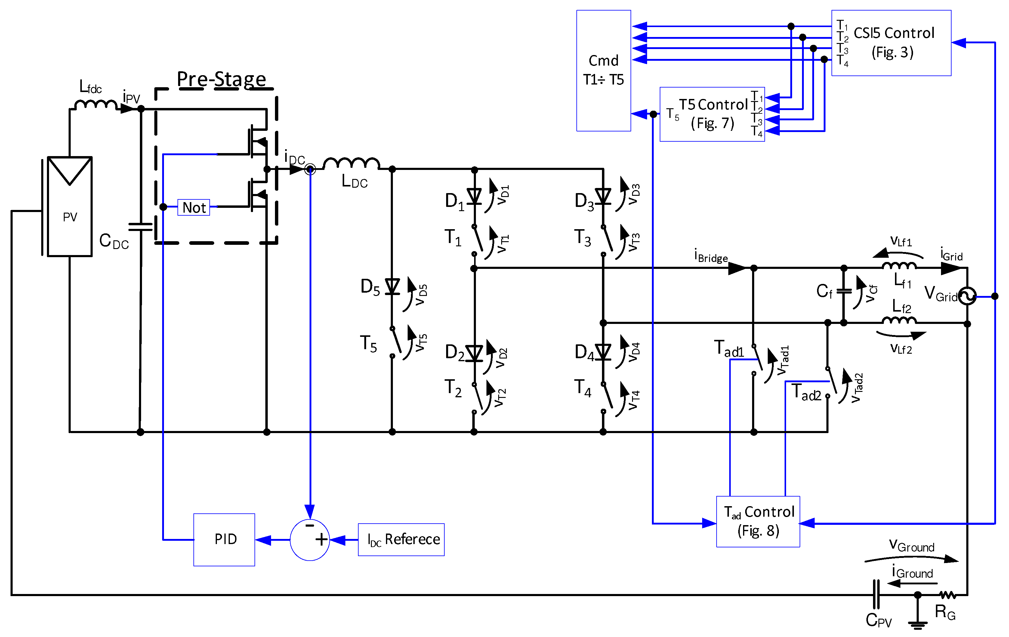
3. Proposed CSI5 Topology
In order to address the main drawback of the CSI topology, two main modifications were performed, which will be detailed in the following.
The first improvement was obtained by adding a switch to the basic CSI topology and obtaining the CSI5 converter, as shown in
Figure 6. The additional power device (
and
) was used to provide the zero state to the output [
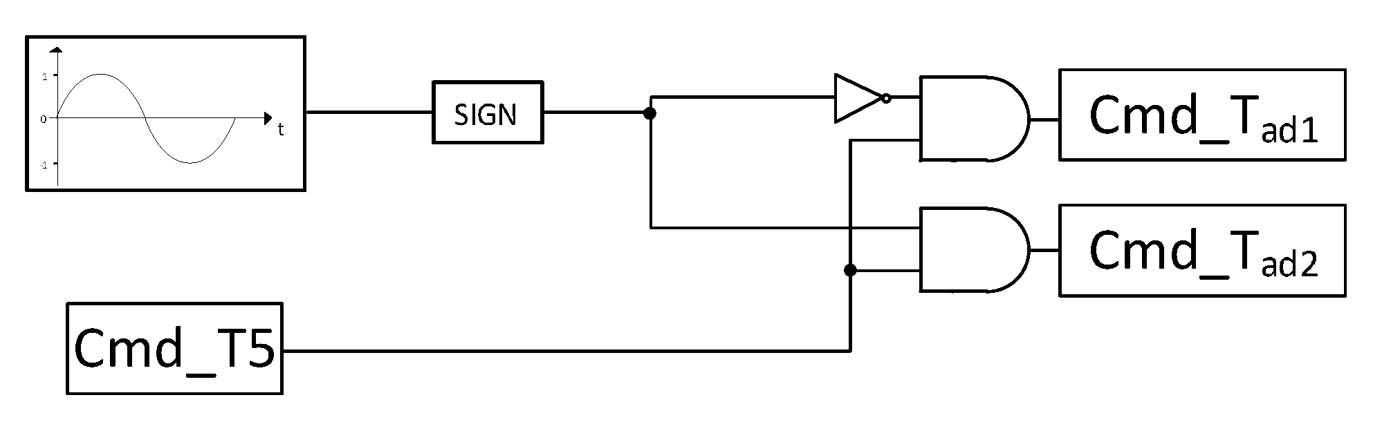
12], strongly reducing the conduction loss of the topology (where only two devices carry the current, instead of four). As a matter of fact, during overlap time, the input current always flows through T5 and D5 instead of one leg of the full-bridge. This way, all commutations of the full-bridge switches are zero-current commutations (ZCS). This results in all the commutations of T5 being hard-switching, but the switching power losses are also concentrated only on this device. In order to maximize the converter efficiency, T5 should be chosen with different criteria than the other transistors—for example, a SiC device would be preferred, but this would come at the price of additional cost. The control for the additional switch T5 is shown in
Figure 7. The efficiency improvement consequent to the addition of the zero-state switch has been addressed in previous works by the authors [
18].
A further modification to the basic CSI topology is also shown in
Figure 6. The two low-power switches,
and
, were adopted to obtain a strong reduction of the ground leakage current.
The operating principle relies on the joint action of T5 and the low-power devices. During the zero state, T5 is on and the H-bridge devices are switched off. This operating point effectively decouples the electrical grid from the DC source, and reduces the ground leakage current. However, the full-bridge output terminals remain floating with respect to the grid generator. For this reason, the two additional switches
and
connect the output terminals to the negative side of the DC panel, with the objective of limiting the high-frequency oscillation across the parasitic capacitance represented by
. Only one of the two additional switches is active for each half-wave:
is used during the positive half-wave, and
during the negative half-wave, respectively. Since some reactive power handling capability is often required for the MICs, a bidirectional device is preferred for the decoupling devices
and
.
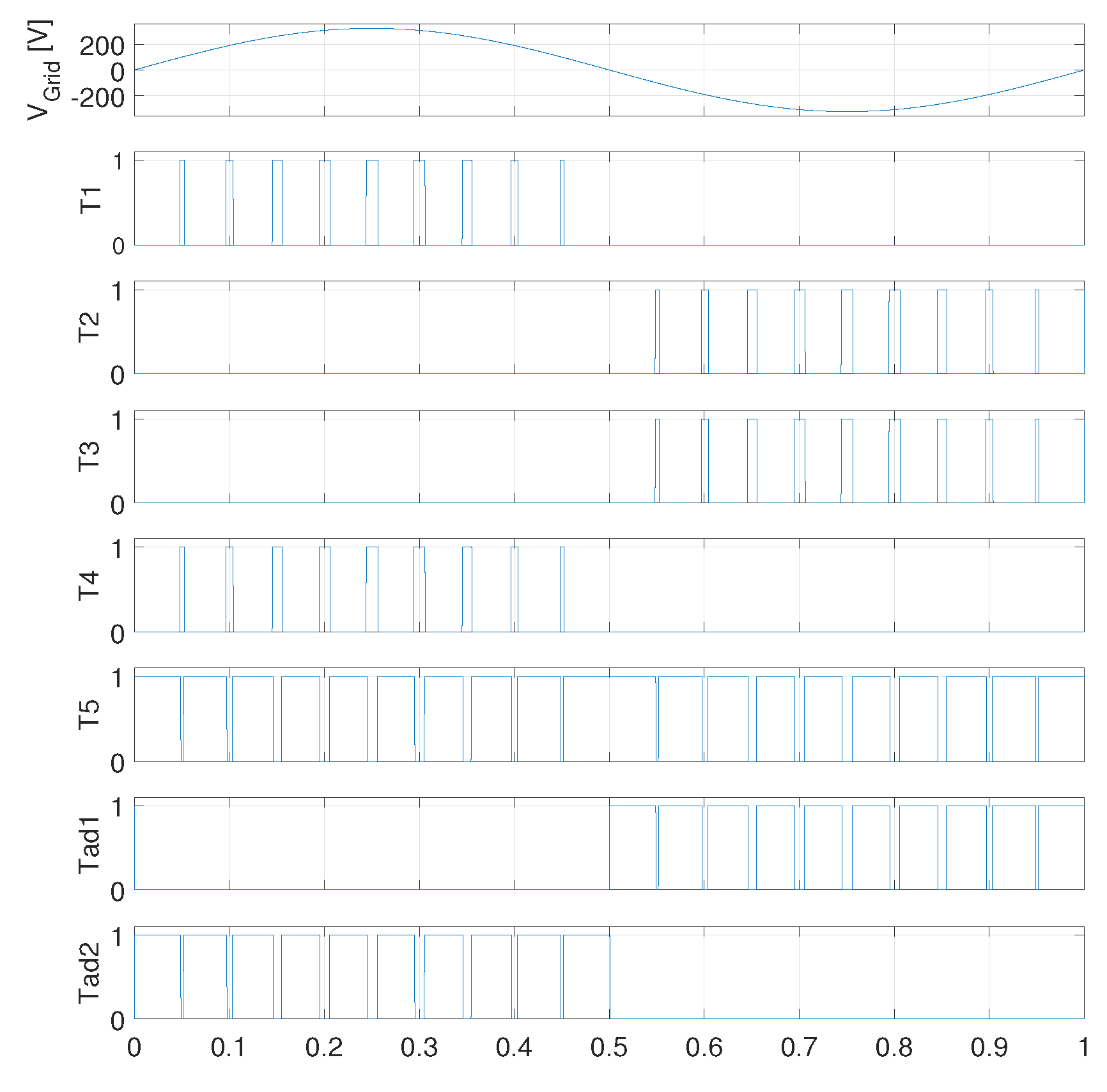
Figure 8 shows the schematic block diagram for the generation of the PWM commands for
and
. For the sake of clarity, the PWM signals for a grid voltage period are depicted in
Figure 9 where all full bridge signals of the CSI5 (T1-T5) and the additional switches (
and
) are shown.
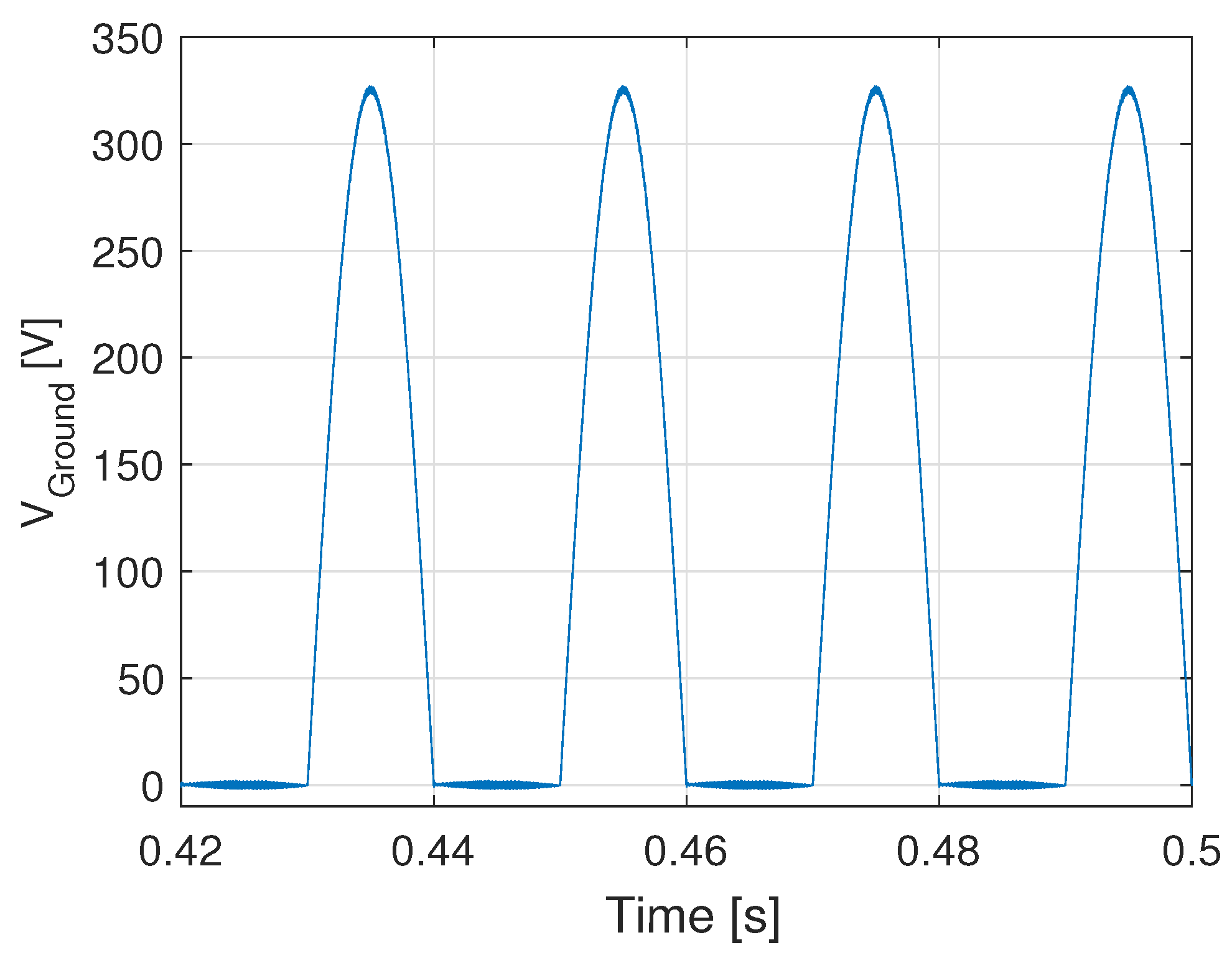
Considering the additional features of the proposed solution, the ground voltage can be computed for all the converter states, and it is detailed in
Table 1.
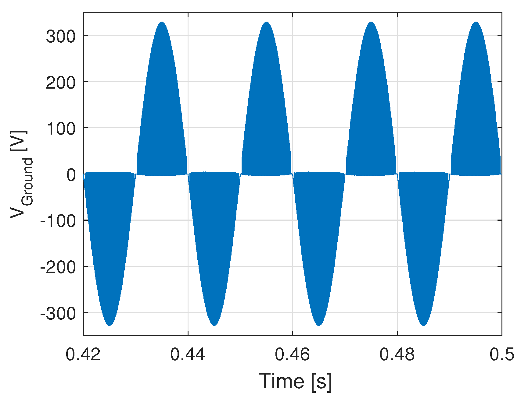
As an example,
Figure 10 shows the expected ground voltage waveform. During the positive half-wave its value is very low, and it is mainly determined by the voltage across the semiconductor devices in on-state and the inductive part of the output filter. During the negative half-wave, the grid voltage shape can be recognized, but without the high-frequency switching components.
The overall control of the proposed solution, considering the pre-stage and the gate signal generation for all devices, is shown in
Figure 11. The ideal current source is substituted by a PV panel and a DC–DC synchronous buck converter.
The task of the pre-stage is to control the CSI inductor current, effectively reducing the inductance requirement for and to decouple the PV source from CSI5. Differently from the three-phase PV CSI, in single-phase operation, the pre-stage is needed in order to manage the fluctuation of the instantaneous electric power output with the mandatory low variations of PV source voltage and current.
Different kinds of converters can be chosen for the pre-stage, and a synchronous buck was chosen for its simplicity. It is to be noted that, for this manuscript, the task of the pre-stage was not to control the input current, since the focus is on the CSI5 topology, and the input current control issues are common to all single-phase PV applications. A DC capacitor was adopted at the input of the pre-stage to reduce the oscillation of the panel operating point. This represents the main drawback for the use in actual PV microinverters of single-phase CSI topologies—to keep the small dimensions and weight, there is the need to manage the output pulsating power through a capacitor. However, different solutions, based on active capacitors [
19], can be employed.
It is worth repeating that a single-phase converter would always need some kind of active decoupling connected either in parallel or in series, to match the different power flow of the panels and grid. It is also worth noting that having a continuous fixed current in the inductor is not necessary, since the current value can be changed even without a front-end [
20], and inductor current oscillation can be compensated for with proper Pulse Area Modulation [
21]. For simplicity’s sake and to better focus on the ground leakage current problem, these aspects have not been introduced in this paper, and a simple DC–DC buck converter is used, although it would not represent a practical application.
4. Simulation Results
The performance and operation of both the basic CSI and the CSI5 topology were assessed and compared via numerical simulations in the PLECS environment. The converter topologies are the same as that showed in
Figure 1 and
Figure 11, and
Table 2 summarizes the simulation parameters.
The control strategy implemented in the simulation environment for the two solutions are those showed in
Figure 2 and
Figure 8 and no additional dedicated power factor correction was employed.
The simulations were carried with four BP365PV panels in series and the parameters are summarized in
Table 3.
The overlap time (see
Figure 3) was inserted before the transition command of every transistor. In the simulations, the modulation index K (see
Figure 2) was kept equal to 0.23. No common-mode filters were introduced in the electric circuit. Without any degradation of the power quality caused by equivalent parasitic capacitance, the injected power into the grid is equal to 221 W.
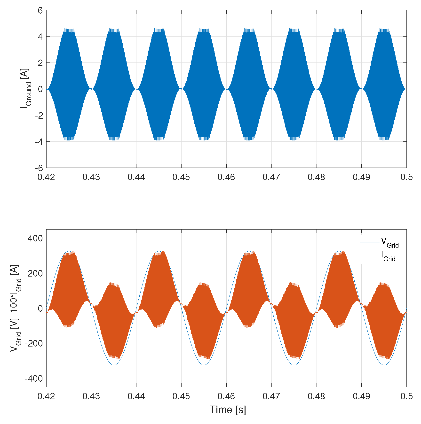
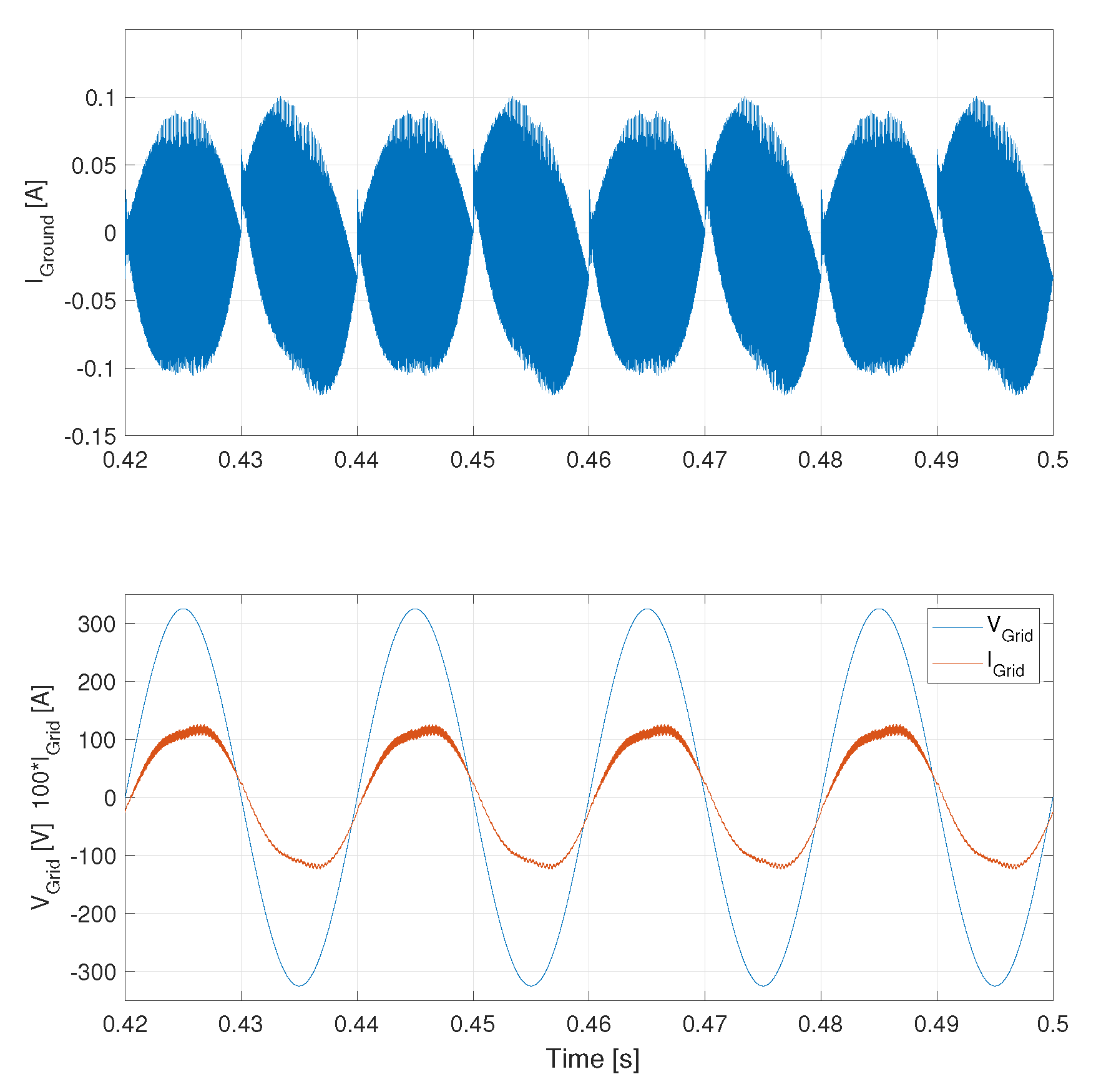
Figure 12 shows that the grid voltage and injected grid current were characterized by a strong distortion due to the presence of an unacceptably high ground leakage current in the case of basic topology.
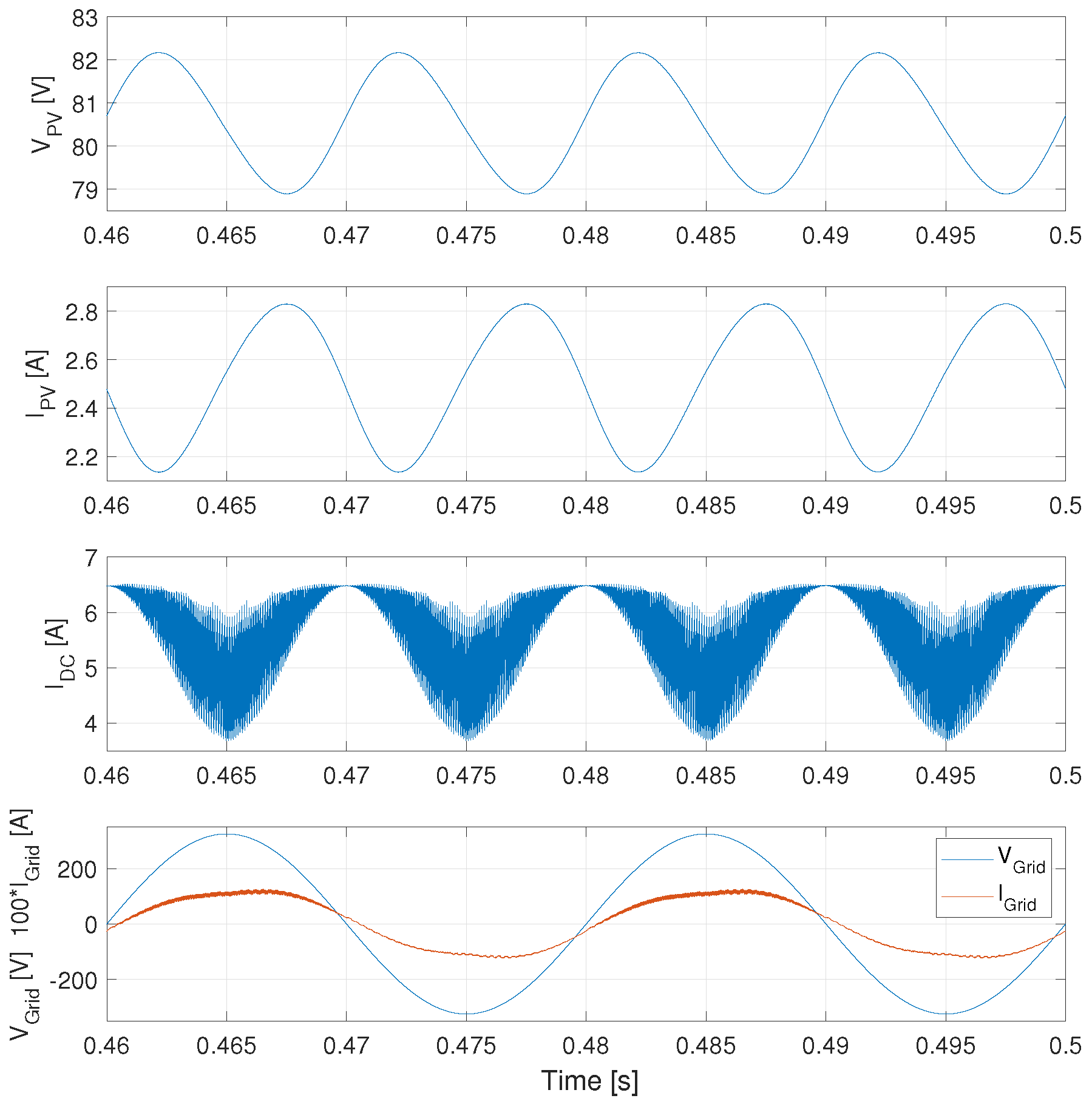
Figure 13 shows the same signals of
Figure 12 in the case of a proposed CSI5 topology. The strong reduction of the ground leakage current is clearly visible, together with noticeably lower distortion in the injected current. The phase displacement of the injected current with respect to the grid voltage is due to the output filter reactive power, as previously discussed. The asymmetry in the peaks of the ground leakage current is caused by the asymmetry of the ground voltage, as described in
Table 1.
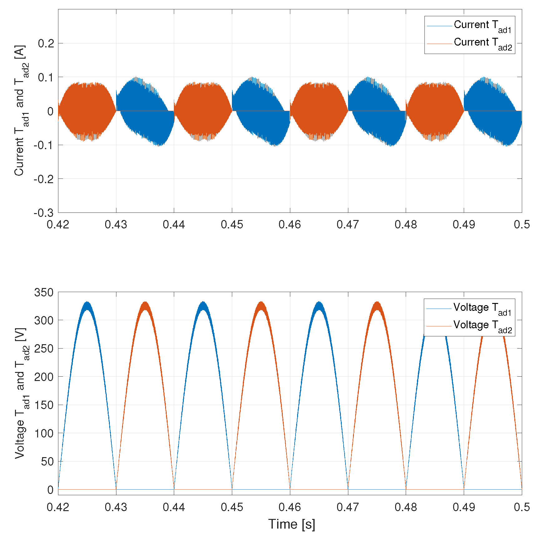
The currents of the clamping switches
and
are very low, as
Figure 14 shows, together with their blocking voltage. The RMS current flowing on
and
are equal to 32 mA
RMS and 27 mA
RMS, respectively. The two current levels are different because of different resulting current paths, shown in
Figure 11.
Another set of simulations was conducted in order to verify the robustness of the CSI5 solution when taking into account the inductance asymmetry between and , such as due to manufacturing tolerances; in particular, considering the worst case scenario with a difference of 20% ( = 450 H and = 550 H), the RMS value of the results are equal to the previous value (50 mARMS), while the RMS current that flowed in and were respectively equal to 30 mARMS and 26 mARMS—the difference is negligible.
Figure 15 shows an acceptable variation of the PV input current that could be exploited for MPP tracking of the PV panel. As it can be seen, the variation of the current that flows in the DC inductance
did not result in excessive distortion in the current waveform injected into the grid. In the case of a larger variation, such as in order to exploit the
inductor for power decoupling, the injected current THD can be kept under control by employing PAM modulation [
22].
5. Low Voltage Experimental Validation
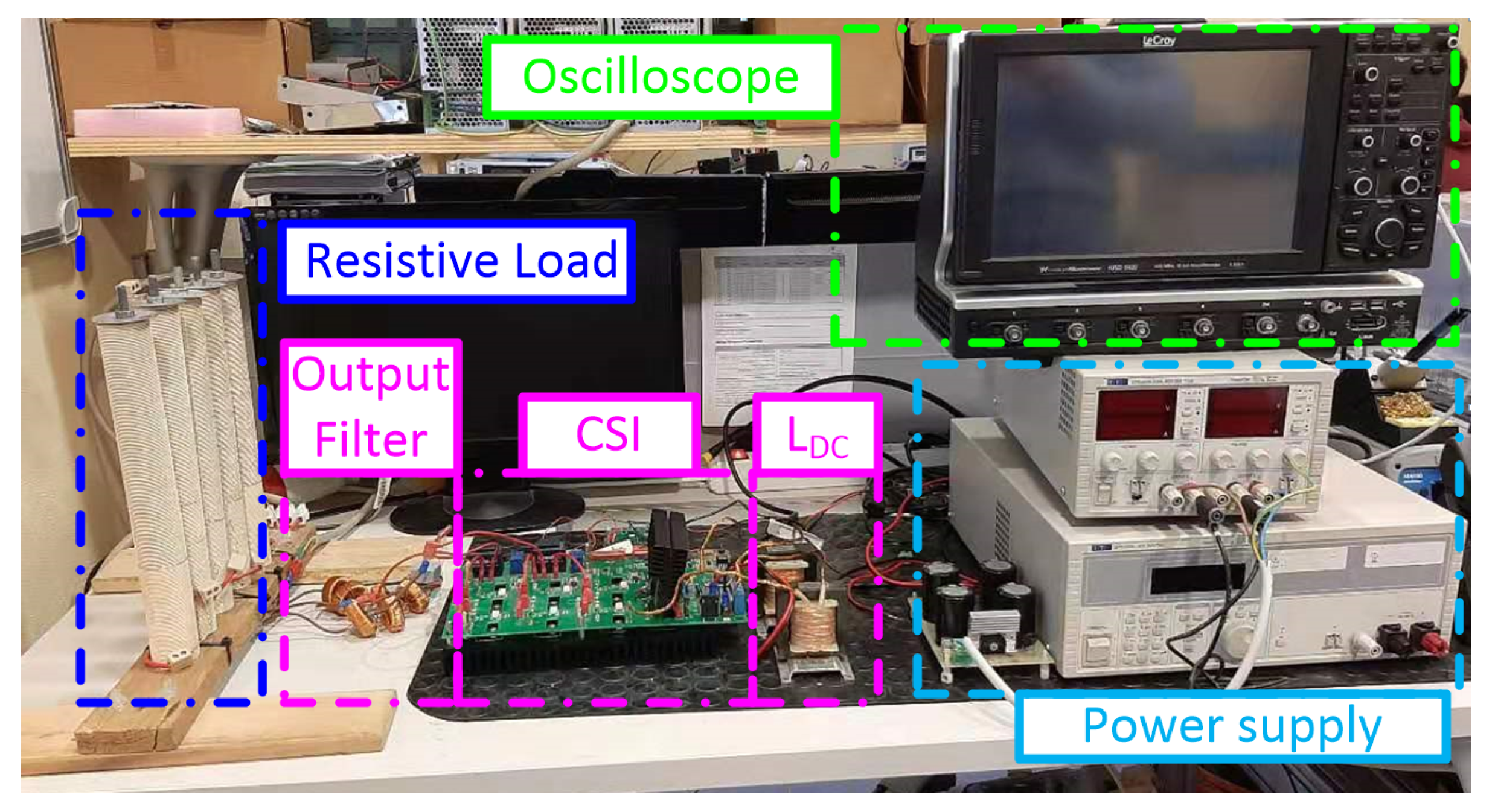
A laboratory scale prototype and test set-up was developed in order to perform experimental measurements of the CSI5 topology with aims of assessing the feasibility of the proposed solution and to validate the ground leakage current capability of CSI5 compared to the basic CSI solution.
Figure 16 shows the experimental test set-up, where the CSI5 solution is realized from an existing three-phase CSI7 converter [
17]. A basic CSI topology is obtained by disabling in the control firmware the additional bidirectional and clamp switches.
Table 4 summarizes the experimental operating parameters.
In the preliminary experimental evaluation, the tests were carried out in stand-alone mode, and the grid was substituted by a load resistor
. The converter was supplied by a DC power supply with a resistor
connected in series in order to emulate the PV source I/V characteristic when operating in current control mode. A capacitor with the value described in
Table 4 connected between the neutral and the negative terminal of the DC supply was used to simulate the effect of the parasitic capacitance. The ground leakage current was measured with a current probe on the wire connecting this capacitor.
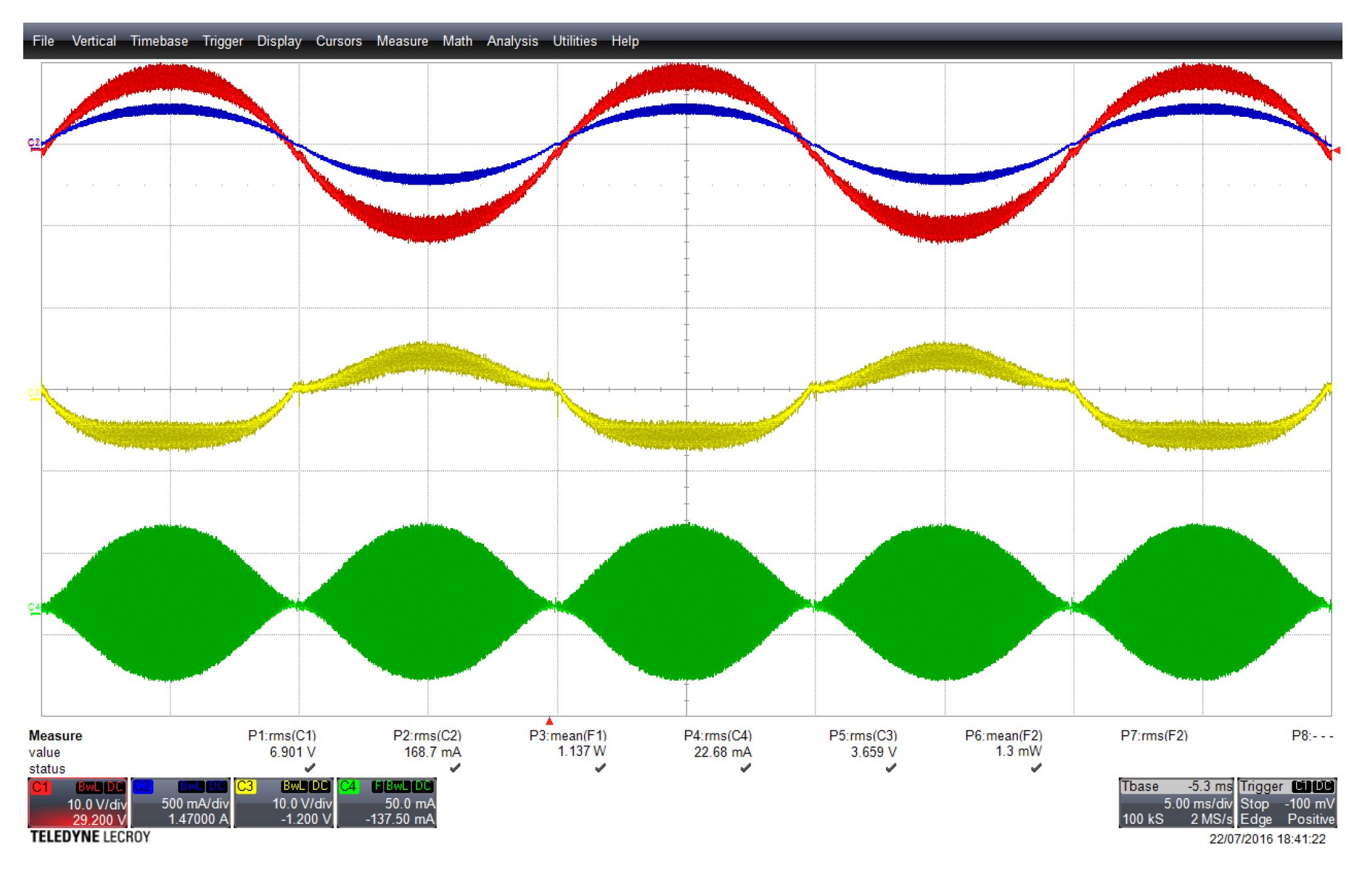
Figure 17 shows the ground leakage current performance of the basic CSI topology. Output voltage and current waveforms, as well as ground voltage and current waveforms are shown. As can be seen, the ground voltage presents large high-frequency components, and the value of ground leakage current is high.
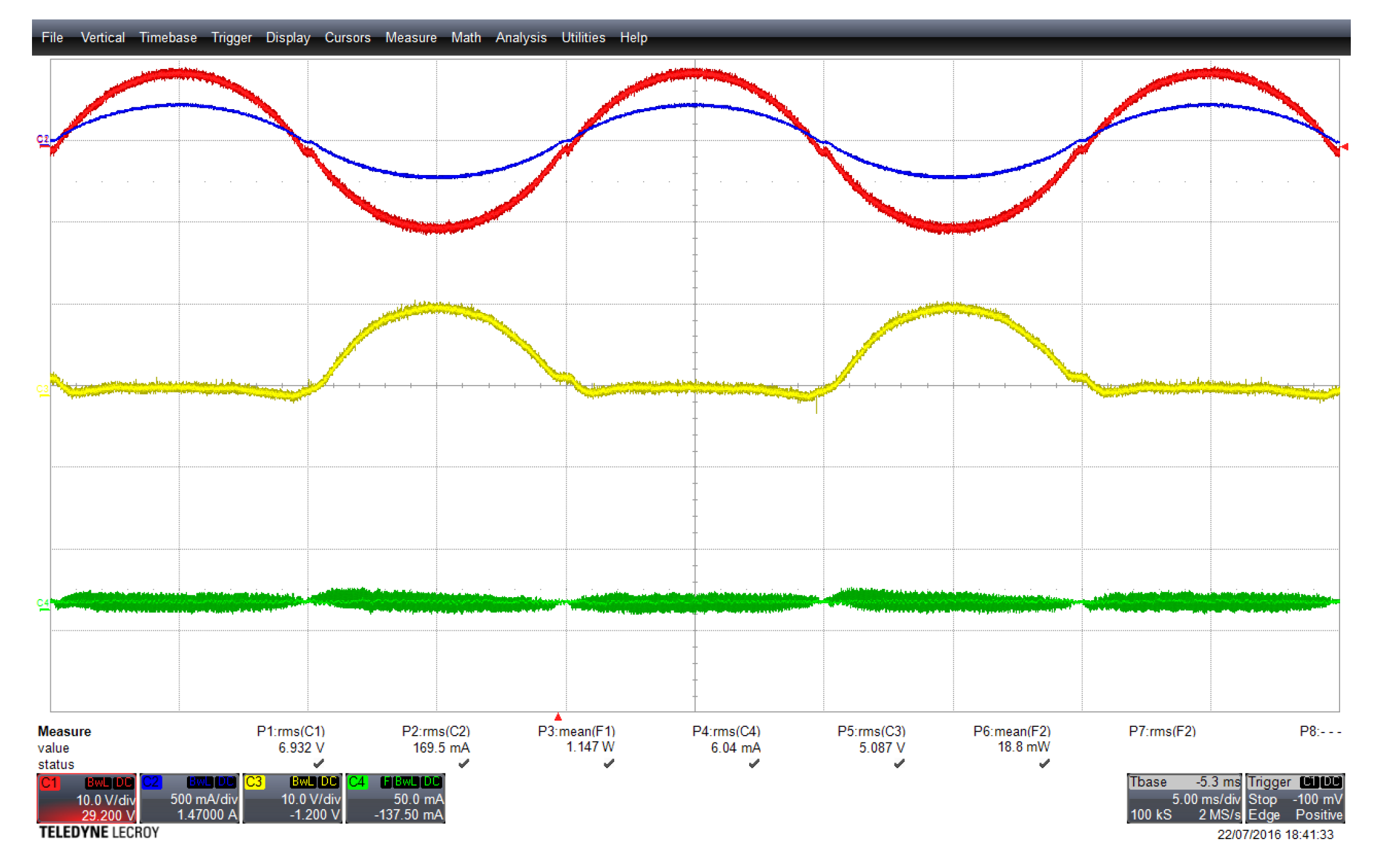
Figure 18 shows the same waveforms of the previous Figure, but with the CSI5 solution without clamping, that is, the presence of the two additional switches
and
. As can be seen, the ground voltage waveform is different than in
Figure 17, and there is a consequent reduction of ground leakage current.
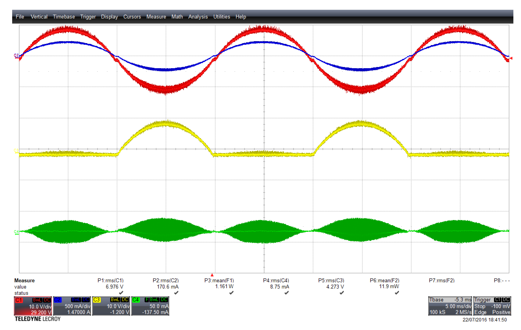
Finally,
Figure 19 shows the relevant results for the proposed solution, that is, CSI5 and the additional clamping switches,
and
. The high-frequency ground voltage oscillation is further reduced, and the ground leakage current is minimized. Overall, the ground current was reduced from 22.7 mARMS to 6 mARMS by adopting the proposed solution.
6. Conclusions
This paper has thoroughly analyzed the main benefits and disadvantages of a novel Current Source Inverter topology, named CSI5, applied to transformerless photovoltaic single-phase systems. The main advantage is the extremely low ground leakage current, demonstrated theoretically, both by simulations and experimental verification and the ease of control. Furthermore, the CSI5 topology presents the intrinsic boost capability of the CSI and the additional switch T5, dedicated to obtain the output zero state and which allows to strongly reduce the conduction losses with respect to the basic CSI topology.
The main drawback, common to all the single-phase integrated converter solutions, is the power matching between the single-phase grid (characterized by a fluctuating power) and the photovoltaic source (characterized by constant power). In order to decouple the DC PV source requiring almost constant current and voltage at MPP and the instantaneous pulsating output power, an additional pre-stage must be inserted for single-phase CSI.
Another aspect that is worth pointing out for future works is that a certain percentage of power decoupling could be obtained by suitably varying the current of the DC input inductor without compromising the THD of the injected current, thanks to the use of the Pulse Area Modulation. To conclude, the CSI5 topology can be employed for module integrated application, although a thorough evaluation of the final application requirement should be carried out to weigh the drawbacks described in this manuscript.


