Article

Light Exposure Effects on the DC Kink of AlGaN/GaN HEMTs

1
Department of Engineering, University of Messina, 98166 Messina, Italy
2
Dipartimento di Scienze Matematiche e Informatiche, Scienze Fisiche e Scienze della Terra, University of Messina, 98166 Messina, Italy
*
Author to whom correspondence should be addressed.
Electronics 2019, 8(6), 698; https://doi.org/10.3390/electronics8060698
Submission received: 14 May 2019 / Revised: 14 June 2019 / Accepted: 19 June 2019 / Published: 21 June 2019
(This article belongs to the Section Microwave and Wireless Communications)

Abstract

:
This paper presents the effects of optical radiation on the behavior of two scaled-gate aluminum gallium nitride/gallium nitride (AlGaN/GaN) high electron mobility transistors (HEMTs). The tested devices, having a gate width of 100 and 200 µm and a gate length of 0.25 µm, were exposed to a laser beam with a wavelength of 404 nm (blue-ray) in order to investigate the main optical effects on the DC characteristics. Owing to the threshold shift and the charge generation, a marked increase of the gate and drain current was noticed. The occurrence of the kink effect in the absence of light exposure was identified, and a hypothesis about its origin is provided. The obtained results agree with the analysis previously carried out on gallium arsenide (GaAs)-based devices.

1. Introduction

Currently, III–V field-effect transistors have demonstrated their suitability to be controlled by an optical signal, which is a fundamental feature in a wide number of applications for telecommunication and high-speed systems [1,2]. In this framework, aluminum gallium nitride/gallium nitride (AlGaN/GaN) high electron mobility transistor (HEMT) technology has stood out for its main characteristics, that is, high breakdown fields, saturation velocity, and operating temperature.
In the scientific literature, limited information can be found about the effects of light on GaN-based HEMT devices [3,4,5]. One of the main issues noticed in AlGaN/GaN HEMTs is the kink effect, a drain current increase at a certain drain-source voltage, VDS, generating an abrupt growth of the output conductance, gDS. The origin of this phenomenon may differ depending upon the employed semiconductors and has been ascribed to (a) the presence of impact ionization generating the accumulation of holes, typical of narrow bandgap semiconductors, and (b) trapping and detrapping effects, typical of wide bandgap semiconductors [3,6,7].
The latter is the case of GaN-based devices in which the trapping phenomena cause a decrease of the number of electrons available for the conduction, with a consequent bending of the drain-source current, IDS [8,9,10,11,12].
Although this is the most validated hypothesis about the origin of the kink effect in GaN-based devices, there is no agreement about the location of the involved traps. Moreover, there is a case where the kink effect has been ascribed to the impact ionization [13]. This suggests that the kink effect origin must be analyzed on a case-by-case basis. In this work, two scaled-gate AlGaN/GaN high electron mobility transistors with a gate width of 100 and 200 µm and a gate length of 0.25 µm were exposed to a laser beam with a wavelength of 404 nm (blue-ray) by means of a properly tailored test-bench.
An extensive experimental analysis of the DC characteristics showed the presence of the kink phenomenon in the absence of laser illumination, and the main changes under light exposure are highlighted. An effective hypothesis about the origin of the kink is provided and the curve modifications in the presence of optical radiation is explained.
The achieved results are in accordance with those obtained for gallium arsenide (GaAs)-based devices exposed to optical radiation [14,15,16,17,18].
The paper is organized as follows. In Section 2, the characteristics of the tested devices are reported, and the measurement optical setup is described. In Section 3, the DC performances of the two HEMTs under light exposure are shown and the relevant involved processes are analyzed. Finally, conclusive remarks are presented in Section 4.

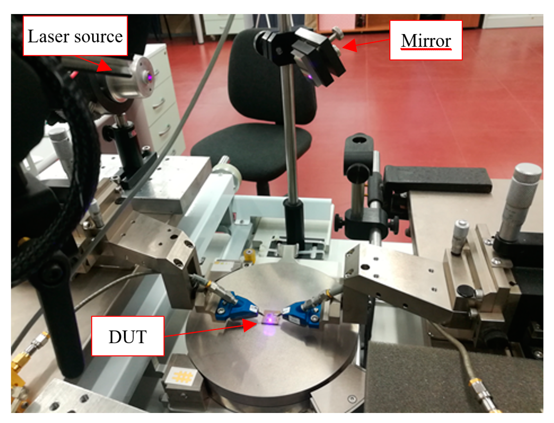
2. The DUTs and the Optical Setup

The devices-under-test (DUTs) were AlGaN/GaN HEMTs on SiC, having a gate width of 100 and 200 µm (2 × 50 and 4 × 50 µm parallel gate fingers, respectively) and a gate length of 0.25 µm.
Two source measure units (SMUs) (Keithley 2611A and 2635A, Tektronix, Beaverton, OR, USA) driven by a proprietary software were connected with the on-wafer probes for tracing the DC characteristics. The employed probes had a central pin for the gate/drain terminal connection and two pins for the ground connection. Thereafter, the input SMU drove the voltage between gate and source, whereas the output SMU drove the voltage between drain and source.
The test-bench was arranged with the aim of illuminating the on-wafer devices from the top side. For this purpose, a blue-ray laser source working at a wavelength of 404 nm was employed. A mirror installed on a micrometric mount was used to focus the laser beam on the sample surface. The micrometric mount allowed the regulation of the beam direction, whose total optical power was equal to 27 mW. Figure 1 presents a picture of the optical setup.
Even though the energy value of the optical source was to some extent lower than the GaN energy gap (3.33 eV), the used laser beam pointed out outstanding effects on the DUT performance.
These effects can probably be ascribed to the concomitant semiconductor processes, such as band-tailing, free-carrier absorption, broadening mechanisms, and photon assisted tunneling, that typically occur when a strong electric field is involved, as for the GaN 2-DEG quantum well of the HEMT (Franz–Keldysh effect) [19,20].
In addition, the presence of dopants modifies the absorption coefficient by leading to a lower energy threshold, thus encouraging the generation of optical charges [21]. Moreover, in order to rule out any effect due to ambient light exposure, ceiling lamps were turned off during the measurements and the windows were darkened. Finally, the measurements were not consecutively performed in order to ensure the same conditions for each measurement step.

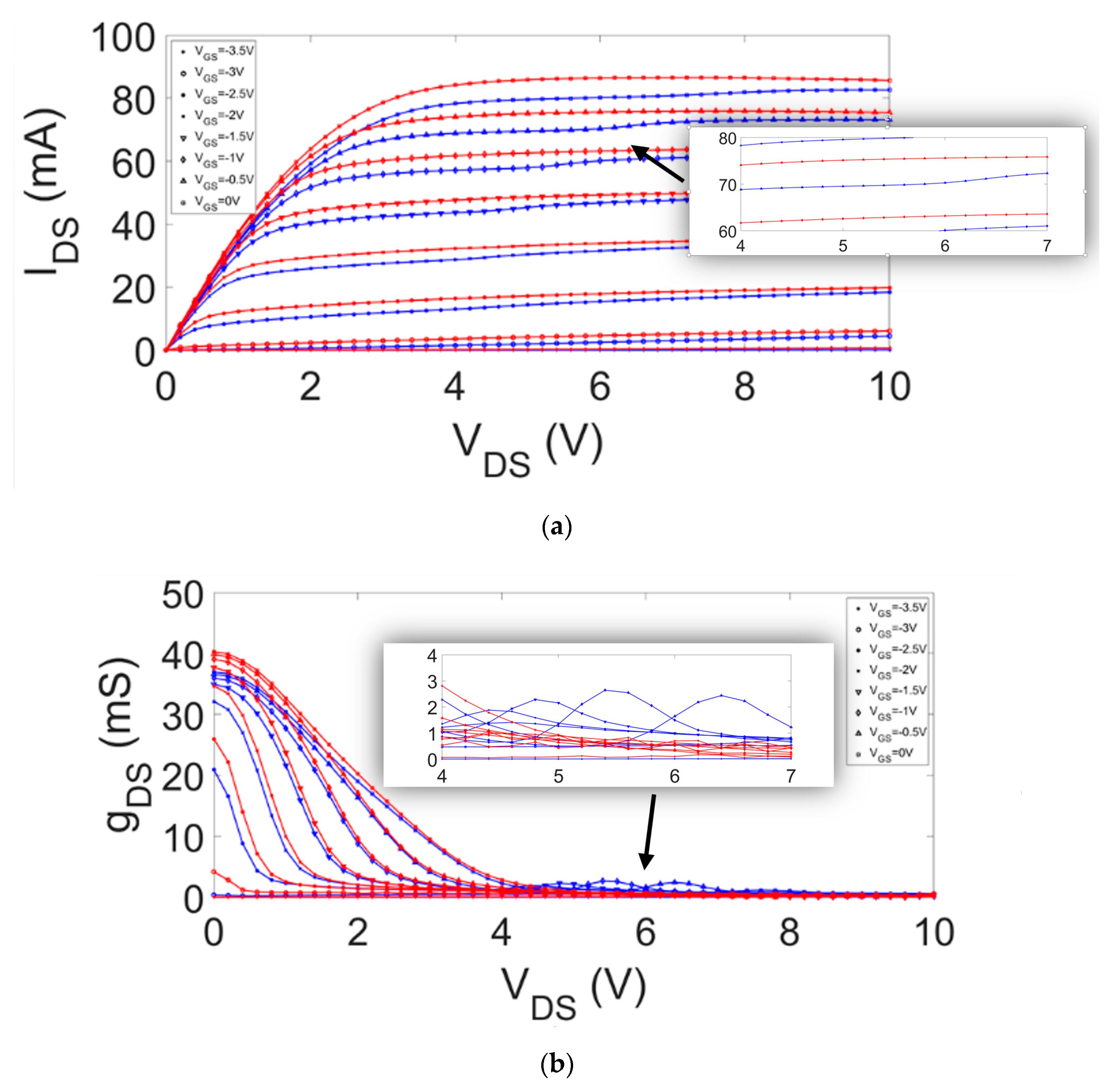
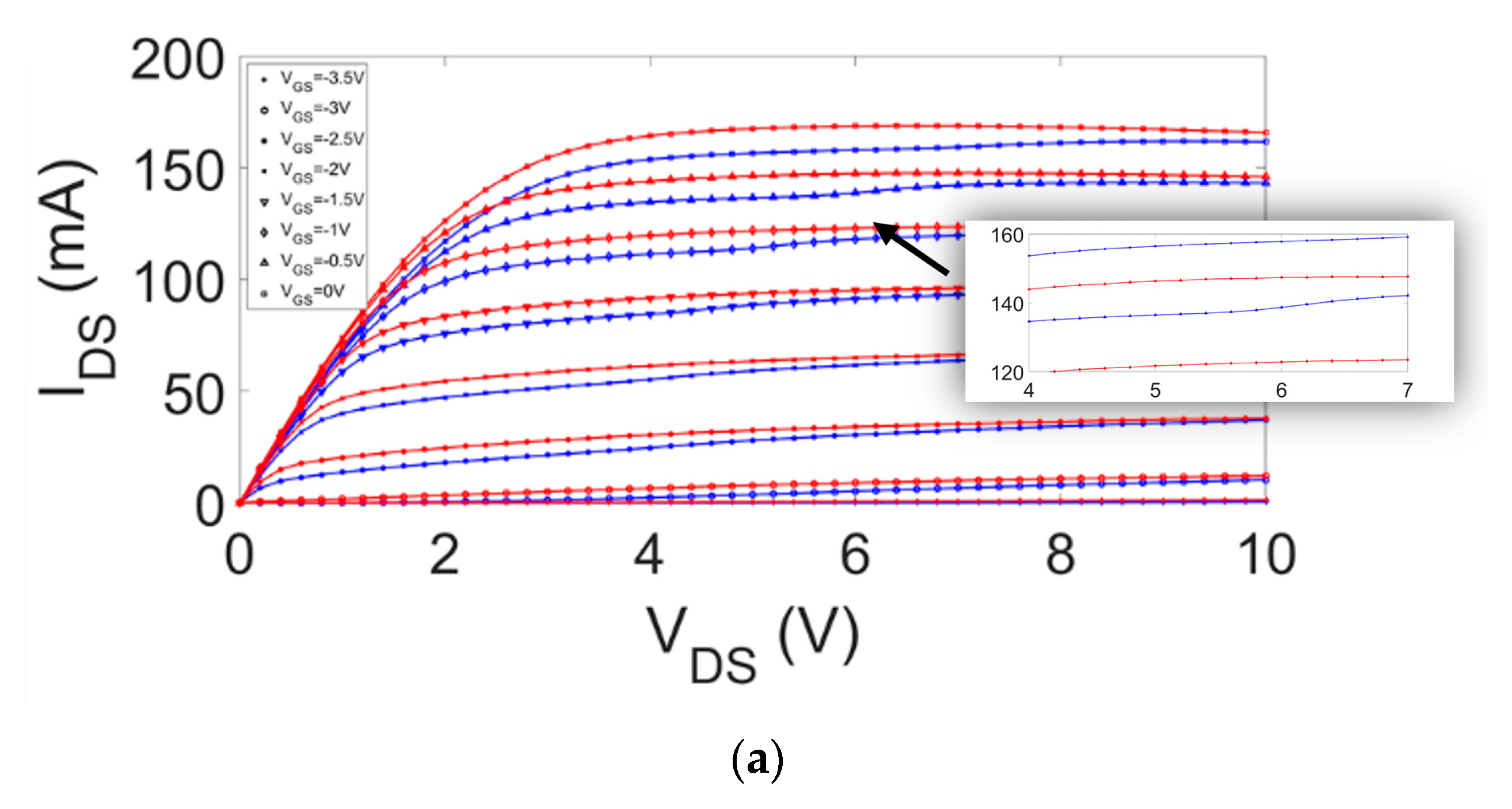
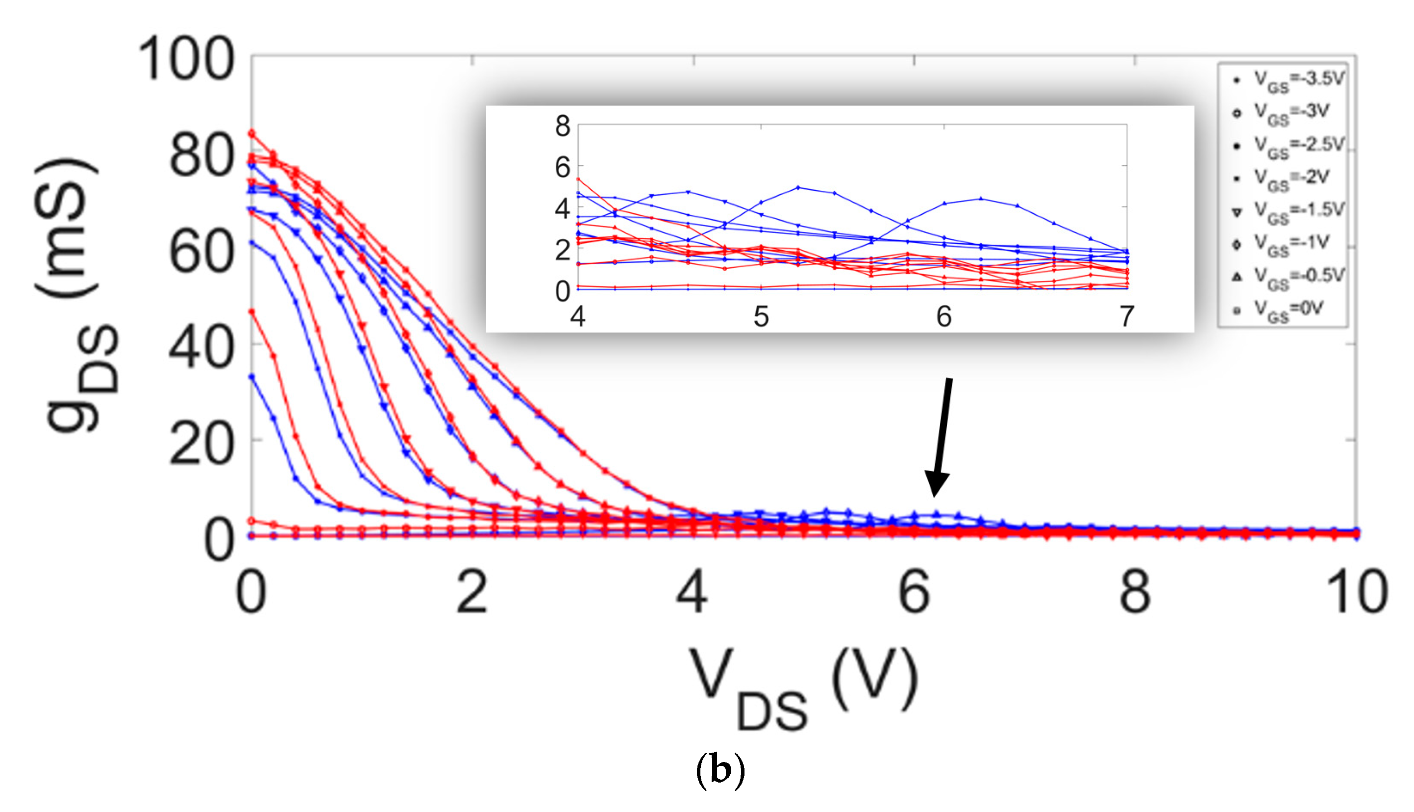
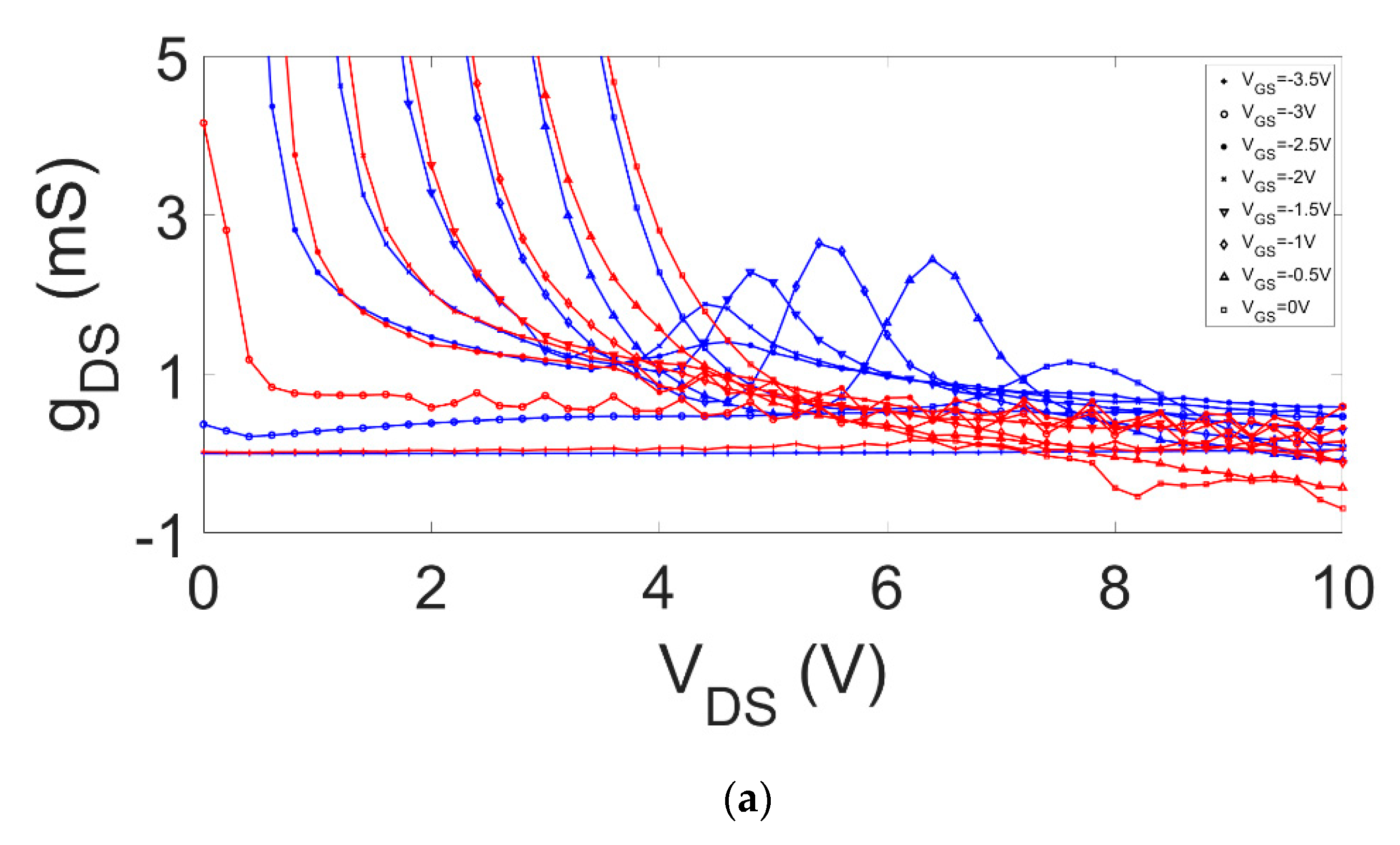
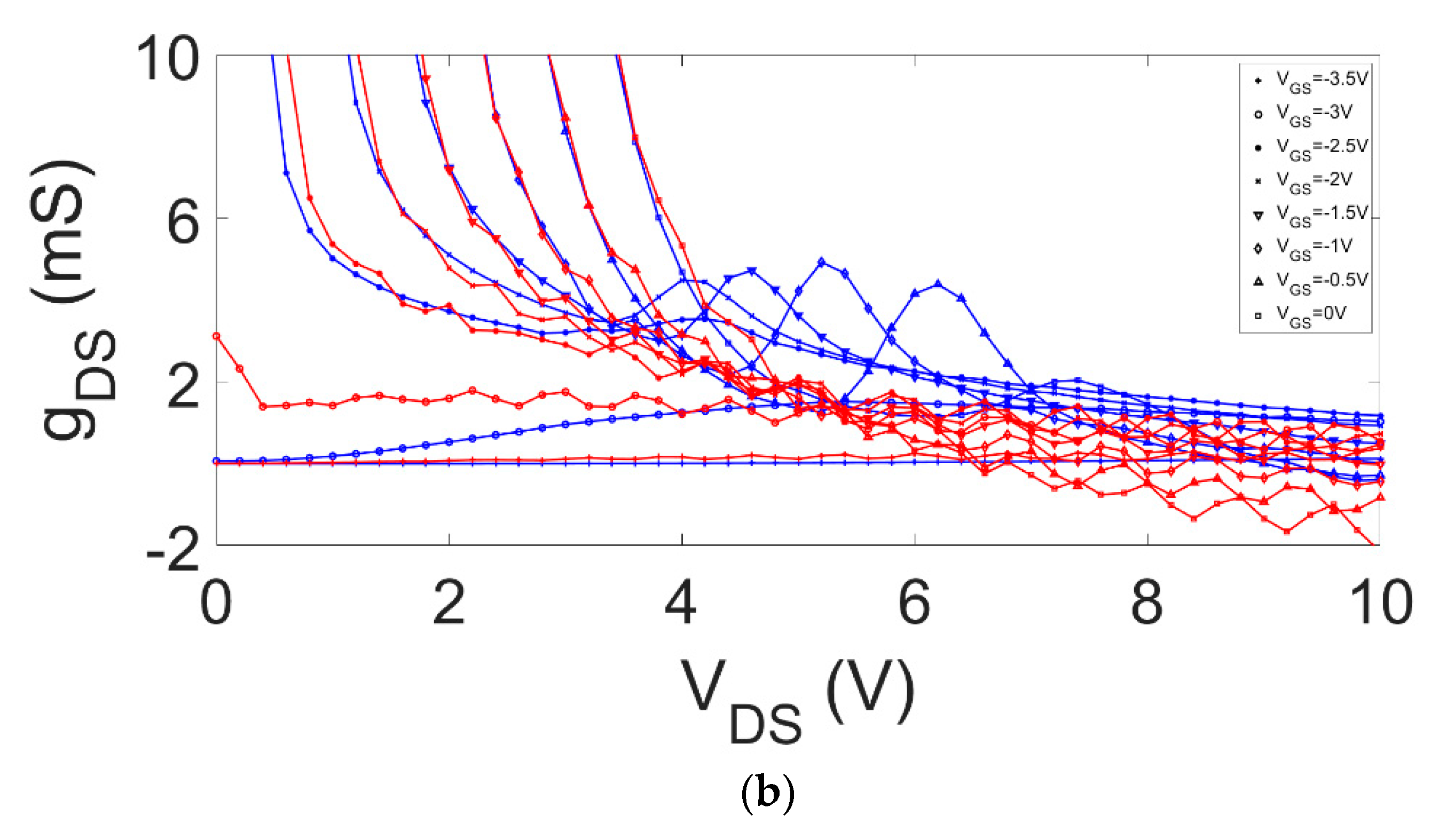
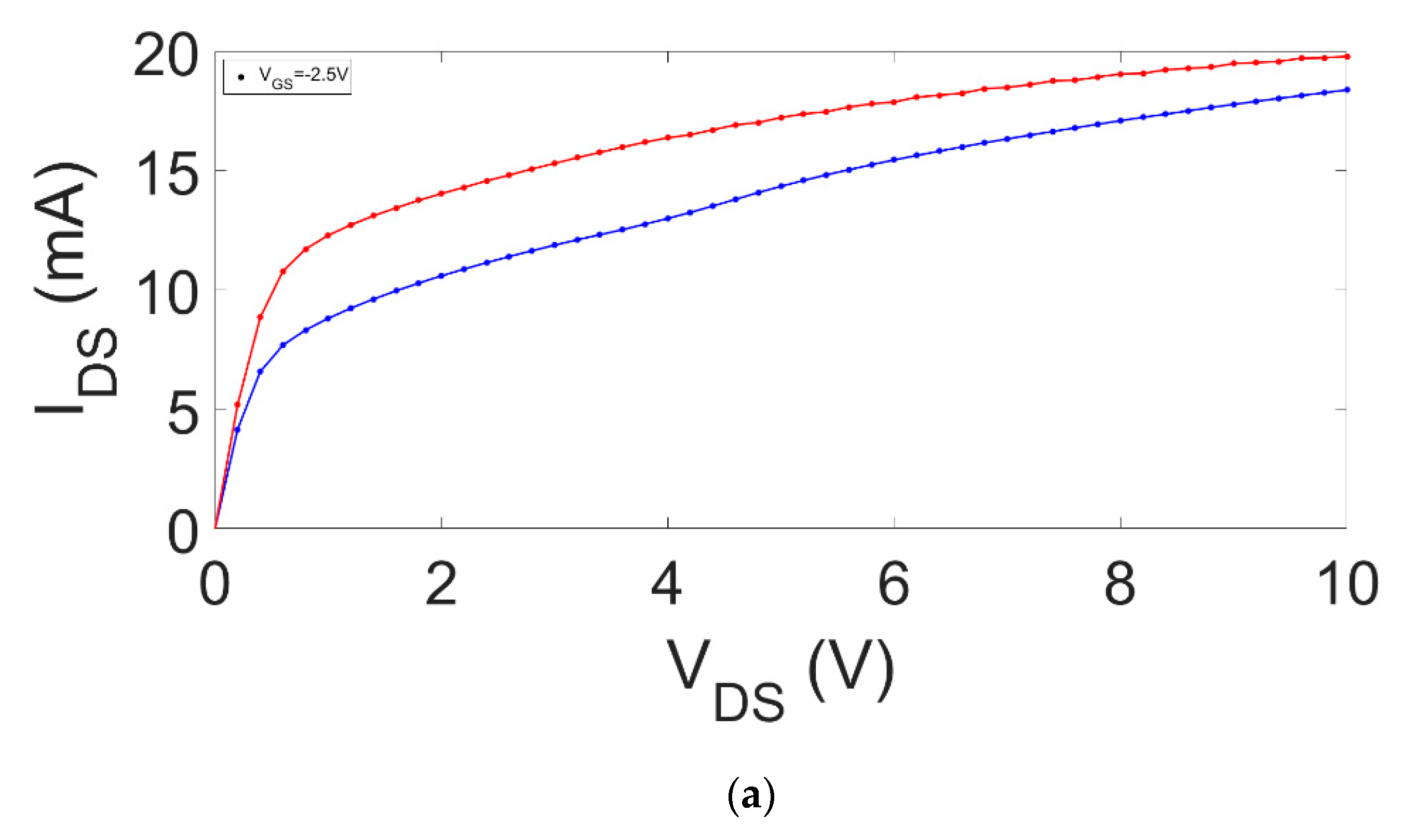
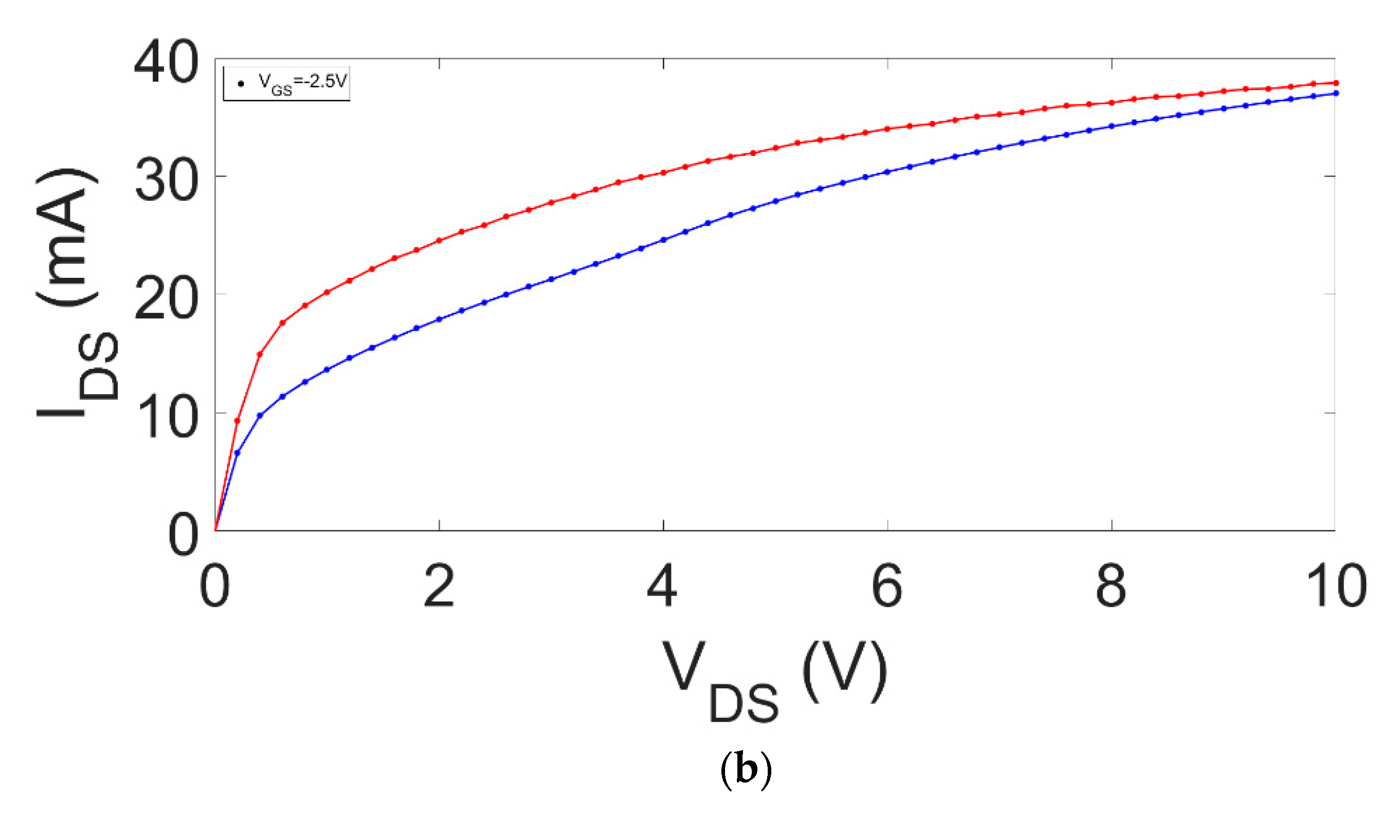
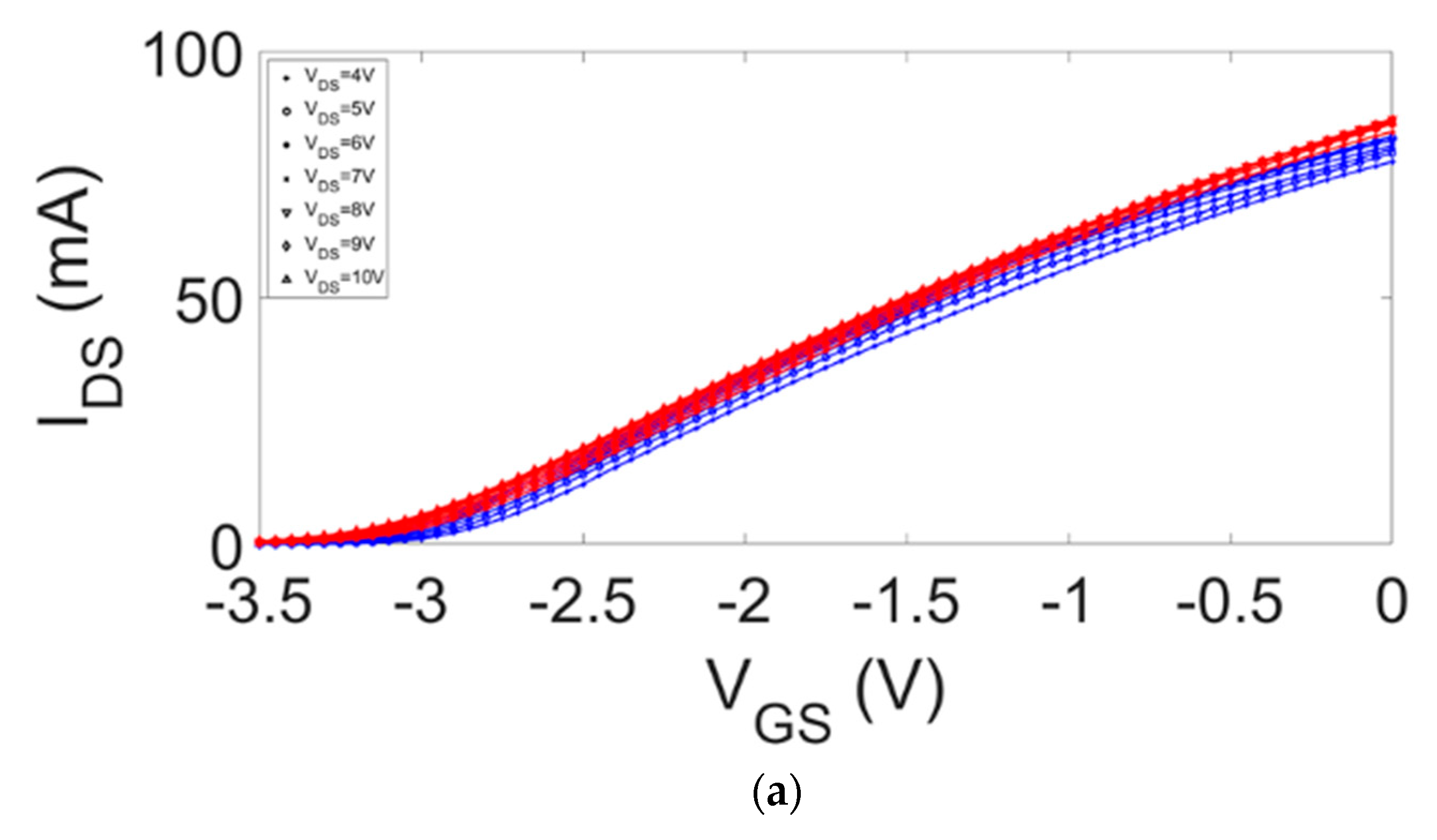
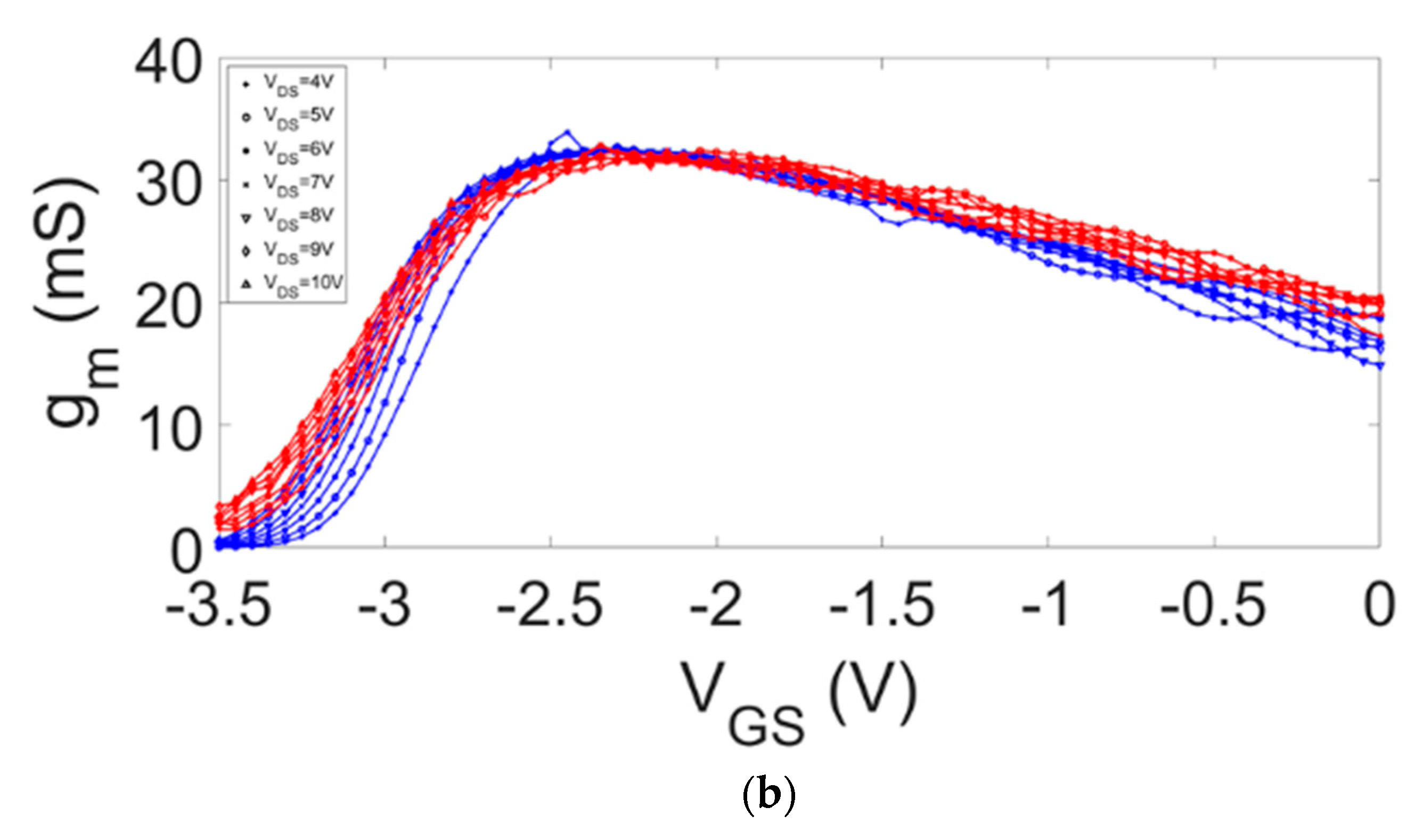
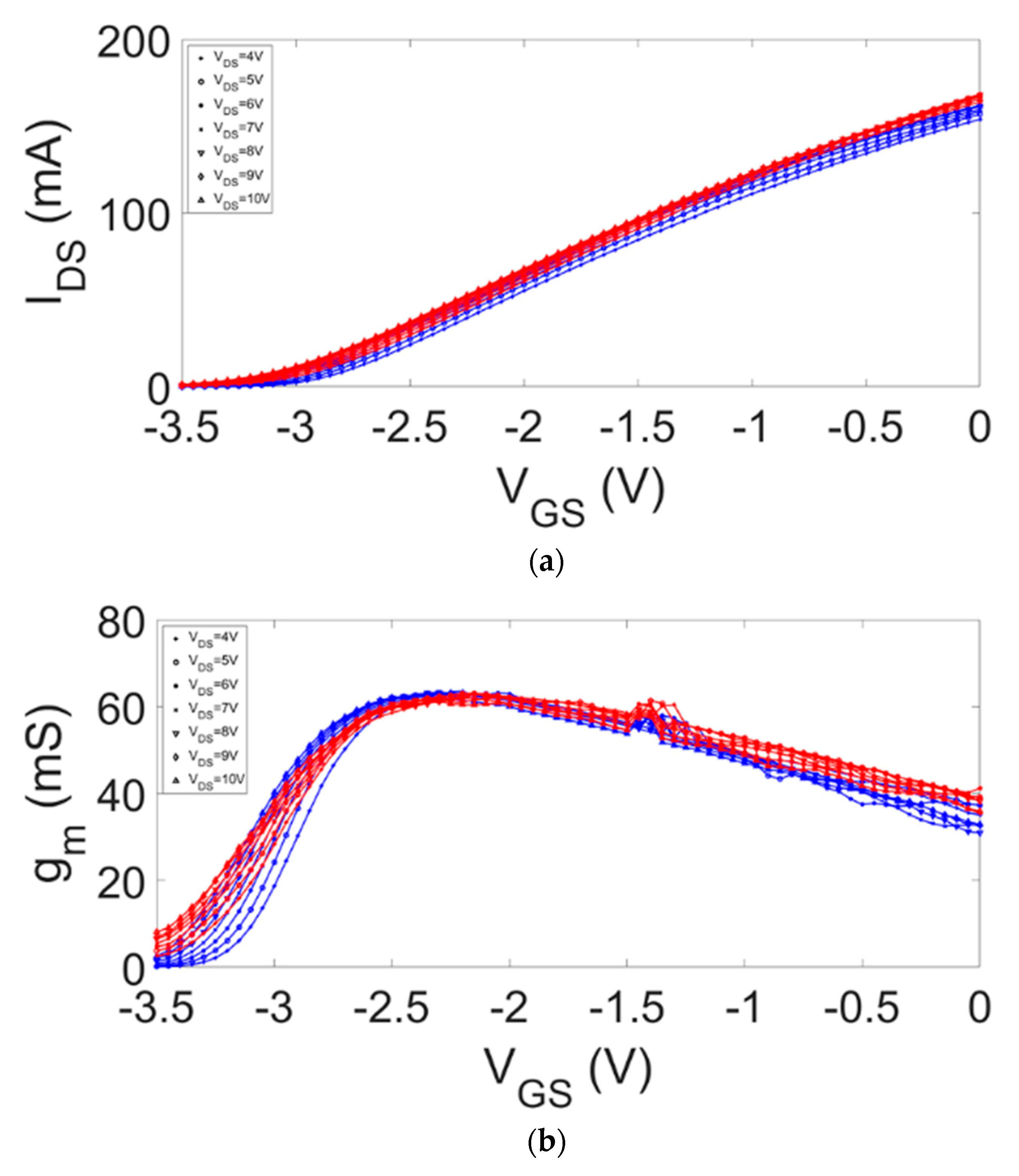
3. AlGaN/GaN HEMTs under Light Exposure

The trend of IDS and the output conductance gDS versus the drain voltage VDS with VGS from −3.5 V to 0 V (step 0.5 V) without laser exposure and under optical radiation are shown in Figure 2 and Figure 3 for the devices with a gate length of 100 and 200 µm, respectively.
For both devices, a clear kink effect is recognizable either in Figure 2 and Figure 3a, where the typical bending of IDS versus VDS curve appears, or in Figure 2 and Figure 3b, where the trend of gDS versus VDS exhibits a sudden increase for VDS between 4 V and 6 V.
Slight concurrent self-heating effects are likely to occur, especially under light exposure, by observing the output characteristics for both devices. When self-heating processes are involved, a typical down-bending of IDS is observed, as is the case for VDS values higher than 7 V and VGS values between −0.5 V and 0 V.
The occurrence of the self-heating can be noticed from the negative values taken on by the output conductance, as well. The related close-up view curves of gDS for both devices are presented in Figure 4.
By looking at the part of the graph exhibiting negative gDS values, it can be seen that self-heating effects under illumination take place at VDS values higher than the typical kink voltages observed in the dark characteristics. Based on these considerations, the authors infer that the disappearance of the kink is likely due to the optical radiation, as is already known from the scientific literature [3].
The IDSVDS curves without laser exposure exhibit a moderate increase of the current level for “high” VDS (e.g., above VDS = 7 V for VGS = −0.5 V). This effect is a direct consequence of the kink effect. First, trapping mechanisms soften the increase of the IDS with increasing VDS, and then, detrapping processes cause the sudden increase (kink) of the drain current.
From both Figure 2 and Figure 3, it is also evident that the kink effect disappears under light exposure. This behavior may confirm that trapping and detrapping phenomena are involved. Indeed, under light exposure, the photons provide the energy required for the detrapping, eliminating the kink effect and resulting in the increase of the drain current [3]. The effect is also present for higher |VGS| as evidenced in Figure 5, where IDS versus VDS for VGS = −2.5 V (e.g., a higher absolute value of VGS) measured for both the 100 μm and the 200 μm HEMTs without and with laser exposure is reported.
In detail, the effects of the optical radiation influence the IDS curve for values of VDS lower than those of the point where the kink appears, making the drain current higher than under the dark conditions. The blue-ray exposure avoids the electron trapping that typically takes place close to the drain side of the gate, namely where the electric field is higher [8].
Since gDS expresses the variation of IDS versus VDS, its wavy nature is directly related to the kink effect. The rising portion of the wave is due to the increased values of the derivative of IDS versus VDS while detrapping effects presumably occur, whereas the decreasing portion of the wave is due to the saturation of the drain current. The position of the peaks varies according to the different values of the kink voltage.
The internal photovoltaic effect stimulates an excess of photo-generated carriers involving the decrease of the channel potential barrier. This physical mechanism agrees with the analysis previously published when employing GaAs-based devices [14,15,16,17,18]. The threshold voltage shift occurrence is clearly visible in Figure 6 and Figure 7, for the devices with a gate length of 100 and 200 µm, respectively, where IDS and the transconductance gm versus VGS with VDS from 4 V to 10 V (step 1 V) are shown and are clearly shifted under light exposure.
Further evidence of the trapping and detrapping phenomena as the physical origin of the kink can be inferred by examining Figure 8, where the gate current IGS versus VGS with VDS from 1 V to 10 V (step 1 V) measured for (a) the 100 µm HEMT and (b) the 200 μm HEMT without (blue line) and with (red line) laser exposure is reported.
When channel impact ionization processes are involved in kink generation, a typical bell-shaped trend of the gate current IGS is expected. As is shown in Figure 8, this is not the case, thus confirming the hypothesis of the involved field-dependent trapping and detrapping phenomena. The marked increase of IGS discloses also the effects of the charge generation under the gate, stimulated by the light absorption.

4. Conclusions

This paper shows the effects of blue-ray radiation on the performance of two AlGaN/GaN HEMTs with a gate width of 100 and 200 µm and a gate length of 0.25 µm. The main purpose of the work was to observe the relevant effects of light on the DC characteristics. An increase of gate and drain current due to the threshold shift and the charge generation was observed. The occurrence of the kink effect in the absence of light exposure, disappearing when exposed to the optical radiation, was noticed. For the analyzed devices, the physical origin of the kink effect can be attributed to the involved trapping and detrapping phenomena.

Author Contributions

S.P. and C.T., being specialists in the physics field, dealt with the optoelectronic section of the measurement set-up and procedure. A.C. and E.C., being specialists in the electronic engineering field, dealt with the electronic section of the measurement set-up and procedure. All the authors discussed and analyzed the results.

Funding

This research received no external funding.

Conflicts of Interest

The authors declare no conflict of interest.

References

  1. Fujiwaraa, M.; Sasakia, M.; Nagatab, H.; Matsuo, H. Optical control of low frequency noise behavior in cryogenic GaAs junction field effect transistor. Cryogenics 2009, 49, 626–629. [Google Scholar] [CrossRef]
  2. Caddemi, A.; Cardillo, E. Optical control of gain amplifiers at microwave frequencies. In Proceedings of the 2017 Computing and Electromagnetics International Workshop (CEM), Barcelona, Spain, 21–24 June 2017. [Google Scholar]
  3. Meneghesso, G.; Zanon, F.; Uren, M.J.; Zanoni, E. Anomalous kink effect in GaN high electron mobility transistors. IEEE Electron Device Lett. 2009, 30, 100–102. [Google Scholar] [CrossRef]
  4. Liang, Y.; Jia, L.; He, Z.; Fan, Z.; Zhang, Y.; Yang, F. The study of the contribution of the surface and bulk traps to the dynamic Rdson in AlGaN/GaN HEMT by light illumination. Appl. Phys. Lett. 2016, 109, 182103–182106. [Google Scholar] [CrossRef]
  5. Caddemi, A.; Cardillo, E.; Salvo, G.; Patanè, S. Microwave effects of UV light exposure of a GaN HEMT: Measurements and model extraction. Microelectron. Reliab. 2016, 65, 310–317. [Google Scholar] [CrossRef]
  6. Somerville, M.H.; del Álamo, J.A.; Hoke, W. Direct correlation between impact ionization and the kink effect in InAlAs/InGaAs HEMTs. IEEE Electron Device Lett. 1996, 17, 473–475. [Google Scholar] [CrossRef]
  7. Webster, R.T.; Wu, S.; Anwar, A.F.M. Impact ionization in InAlAs/InGaAs/InAlAs HEMTs. IEEE Electron Device Lett. 2000, 21, 1935. [Google Scholar] [CrossRef]
  8. Cuerdo, R.; Pei, Y.; Chen, Z.; Keller, S.; DenBaars, S.P.; Calle, F.; Mishra, U.K. The kink effect at cryogenic temperatures in deep submicron AlGaN/GaN HEMTs. IEEE Electron Device Lett. 2009, 30, 209–212. [Google Scholar] [CrossRef]
  9. Birafane, A.; Aflaki, P.; Kouki, A.B.; Ghannouchi, F.M. Enhanced DC model for GaN HEMT transistors with built-in thermal and trapping effects. Solid State Electron. 2012, 76, 77–83. [Google Scholar] [CrossRef]
  10. Jarndal, A.; Ghannouchi, F.M. Improved modeling of GaN HEMTs for predicting thermal and trapping-induced-kink effects. Solid State Electron. 2016, 123, 19–25. [Google Scholar] [CrossRef]
  11. Kaushik, J.K.; Balakrishnan, V.R.; Panwar, B.S. Muralidharan On the origin of kink effect in current–voltage characteristics of AlGaN/GaN high electron mobility transistors. IEEE Trans. Electron Devices 2013, 60, 3351–3357. [Google Scholar] [CrossRef]
  12. Singh, M.; Uren, M.J.; Martin, T.; Karboyan, S.; Chandrasekar, H.; Kuball, M. Kink in AlGaN/GaN-HEMTs: Floating buffer model. IEEE Trans. Electron Devices 2018, 65, 374653. [Google Scholar] [CrossRef]
  13. Brar, B.; Boutros, K.; DeWames, R.E.; Tilak, V.; Shealy, R.; Eastman, L. Impact ionization in high performance AlGaN/GaN HEMTs. In Proceedings of the IEEE Lester Eastman Conference on High Performance Devices, Newark, DE, USA, 6–8 August 2002. [Google Scholar]
  14. Caddemi, A.; Cardillo, E.; Crupi, G. Light activation of noise at microwave frequencies: A study on scaled GaAs HEMT’s. IET Circ. Device Syst. 2018, 12, 242–248. [Google Scholar] [CrossRef]
  15. Takanashi, Y.; Takahata, K.; Muramoto, Y. Characteristics of InAlAs/InGaAs high-electron mobility transistors under illumination with modulated light. IEEE Trans. Electron Devices 1999, 46, 2271–2277. [Google Scholar] [CrossRef]
  16. Caddemi, A.; Cardillo, E.; Crupi, G. Comparative Analysis of Microwave Low-Noise Amplifiers under Laser Illumination. Microw. Opt. Technol. Lett. 2016, 58, 2437–2443. [Google Scholar] [CrossRef]
  17. Chiu, H.-C.; Lin, C.-K.; Lin, C.-W.; Chen, M.-Y. Enhanced optical responsivity of InAlAs/InGaAs metamorphic high mobility electron mobility using indium tin oxide transparent gate technology. Appl. Phys. Lett. 2008, 93, 43506–43508. [Google Scholar] [CrossRef]
  18. Caddemi, A.; Cardillo, E.; Patanè, S.; Triolo, C. An accurate experimental investigation of an optical sensing microwave amplifier. IEEE Sens. J. 2018, 18, 9214–9221. [Google Scholar] [CrossRef]
  19. Osinski, M.; Eliseev, P.G.; Perlin, P.; Lee, J.; Sato, H.; Sugahara, T.; Naoi, Y.; Sakai, S. Anomalous temperature behavior and band tailing in InGaN/GaN heterostructures grown on sapphire by MOCVD. In Proceedings of the Conference on Lasers and Electro-Optics Europe-Technical Digest, San Francisco, CA, USA, 3–8 May 1998. [Google Scholar]
  20. Turkulets, Y.; Shalisha, I. Franz-Keldysh effect in semiconductor built-in fields: Doping concentration space charge region characterization. J. Appl. Phys. 2018, 124, 075102. [Google Scholar] [CrossRef]
  21. Šantìc, B.; Scholz, F. On the evaluation of optical parameters of a thin semiconductor film from transmission spectra, and application to GaN films. Meas. J. Technol. 2008, 19, 105303. [Google Scholar] [CrossRef]
Figure 1. Picture of the optical setup.
Electronics 08 00698 g001
Figure 2. (a) IDS and (b) gDS versus VDS with VGS from −3.5 V to 0 V (step 0.5 V) measured for the 100 µm high electron mobility transistor (HEMT) without (blue line) and with (red line) laser exposure.
Electronics 08 00698 g002
Figure 3. (a) IDS and (b) gDS versus VDS with VGS from −3.5 V to 0 V (step 0.5 V) measured for the 200 µm HEMT without (blue line) and with (red line) laser exposure.
Electronics 08 00698 g003aElectronics 08 00698 g003b
Figure 4. Close-up view curves of gDS versus VDS with VGS from −3.5 V to 0 V (step 0.5 V) measured for (a) the 100 µm HEMT and (b) the 200 µm HEMT without (blue line) and with (red line) laser exposure.
Electronics 08 00698 g004aElectronics 08 00698 g004b
Figure 5. IDS versus VDS for VGS = −2.5 V measured for (a) the 100 µm HEMT and (b) the 200 µm HEMT without (blue line) and with (red line) laser exposure.
Electronics 08 00698 g005aElectronics 08 00698 g005b
Figure 6. (a) IDS and (b) gm versus VGS with VDS from 4 V to 10 V (step 1 V) measured for the 100 µm HEMT without (blue line) and with (red line) laser exposure.
Electronics 08 00698 g006aElectronics 08 00698 g006b
Figure 7. (a) IDS and (b) gm versus VGS with VDS from 4 V to 10 V (step 1 V) measured for the 200 µm HEMT without (blue line) and with (red line) laser exposure.
Electronics 08 00698 g007
Figure 8. IGS versus VGS with VDS from 1 V to 10 V (step 1 V) measured for (a) the 100 μm HEMT and (b) the 200 µm HEMT without (blue line) and with (red line) laser exposure.
Electronics 08 00698 g008

