1. Introduction
The Z-source inverter (ZSI) was introduced in 2003 [
1]. It was claimed that the converter overcomes the conceptual and theoretical barriers and limitations of the traditional voltage-source inverter (VSI) and current-source (CS) inverter and provides a novel power conversion concept. ZSI utilizes the shoot-through (ST) cross-conduction states to boost the input dc-voltage by switching on both the top and bottom switches of at least one inverter leg. ZSI can buck-boost voltage, minimize component count, increase efficiency, and reduce the cost. This topology also has no forbidden switching states, which improves converter reliability significantly.
This solution is intended for various fields of application: dc-dc, ac-dc, ac-ac, and dc-ac. In particular, it is suitable for grid integration or electric drive control [
1,
2,
3,
4]. Further, the quasi-Z-source (qZS) network was proposed in [
2]. As compared to the Z-source (ZS) network, it has a continuous conduction mode (CCM) of the input current. Also, the volume of the capacitors may be lower in the qZS network. Due to these features, ZS and qZS networks have been named as the most suitable solution for renewable energy applications. Many papers have studied in detail possibilities for such applications [
5,
6,
7]. Steady-state analysis and dynamic analysis along with different control strategies have been described in detail [
8,
9,
10,
11,
12,
13,
14,
15,
16,
17,
18,
19,
20,
21,
22,
23,
24,
25].
Since then, many derivative topologies of impedance source (IS) networks have been presented. The main justification of the presented solutions is that they overcome drawbacks of the ZS and qZS networks. Mostly, the benefit is in the low dc-link utilization under constant boost control [
15,
16,
17,
18,
19,
20,
21,
22,
23,
24,
25].
References [
26,
27,
28,
29,
30,
31,
32] present a good overview of existing solutions. Almost all the presented novel solutions are based on the magnetically coupled inductors. The main hypothesis in those papers addresses possible reductions of size and volumes of passive components due to the increase in the turns ratio in magnetically coupled elements. At the same time, the overall conclusions and predictions seem to be incomplete. These papers are devoted to very general issues related to the gain factor, and the number of active and passive components.
After an in-depth overview of the comparative papers, some contradictory results can be underlined. As a result of a direct comparison between novel and conventional solutions, the conclusions reached contain high uncertainty [
33,
34,
35,
36,
37,
38,
39]. Several papers reveal only superior performance of the IS-based converters over conventional solutions [
33,
34,
35]. At the same time, other papers reveal opposite results. In conclusion, despite many studies devoted to the IS derived converters, there are still many open questions.
This research work focuses on the comparison between each other by overall dimensions and voltage stress on semiconductors. A comprehensive comparative analysis is provided for all key types of IS networks with conventional solutions for the dc-dc and the dc-ac application. Conventional solutions based on the boost dc-dc converter will be considered as well (
Figure 1a).
The paper is organized as follows.
Section 2 presents a brief overview of IS derived converters.
Section 3 describes a comparative analysis approach while
Section 4 represents results of comparison.
Section 5 is devoted to the pros and cons discussions of IS networks application in galvanically isolated converters. Simulation and experimental study is summarized in
Section 6. Finally, conclusions are presented and discussed in
Section 7.
2. Brief Overview of IS Derived Converters
Over 20 different types of IS networks subdivided into subgroups have been presented. They may have separated inductors, magnetically coupled inductors, or transformers. Implementation of magnetically coupled inductors or transformers in the IS network can result in a higher voltage boost factor due to the turns ratio. All IS networks can also be divided into those with discontinuous input current and continuous input current (CIC). At the same time, it has been shown that networks with discontinuous input current have no advantage over topologies that have CIC [
30].
Figure 1 shows basic IS networks. The conventional boost converter is presented in
Figure 1a as a reference solution that provides the same functionality. Another reason of including the conventional solution here is that some research results claim that novel IS networks have unconditional advantages over the boost converter [
33,
34,
35].
The first IS network under consideration was the qZS network (
Figure 1b). As mentioned above, it has a CIC and the same size and volume of passive components as for ZSI. The other four selected topologies belonged to the magnetically coupled IS networks [
29,
30,
31]. Since any magnetically coupled inductor can be represented as a combination of leakage inductance, magnetizing inductance, and ideal transformer, any other IS network with a magnetically coupled inductor can be considered a derivation of the above solutions. This was very well demonstrated in [
38].
The trans (T)-quasi-Z-source network (
Figure 1c) with a CIC was the first network with coupled inductors under consideration [
40,
41,
42,
43,
44,
45,
46,
47]. As it was shown in [
47], despite an additional capacitor, the overall size of capacitors is lower. The quasi-T-source network (
Figure 1d) has a CIC and a slightly different configuration.
LCCT networks (
Figure 1f) have quite similar features [
48]. At the same time, many derivative circuits and types of converters are proposed in [
49,
50,
51,
52,
53]. Finally, the A-source network (
Figure 1e) was one of the latest solutions proposed and will be compared as well [
54,
55].
The main advantage of all magnetically coupled derived IS networks is the high boost due to the high turns ratio of the transformer. As a result, the ST duty cycle is shorter. At the same time, no studies have demonstrated the impact of the shorter ST duty cycle on the size, volume, and probable cost of the converter.
3. Comparative Analysis Approach
The two possible applications of any IS network are shown in
Figure 2. In the dc-dc application, the dc-link voltage is close to the peak voltage across the IS network (
Figure 2a). At the same time, the dc-ac converter based on the IS network has no direct dc-link. When the load terminals are shorted through both the upper and lower semiconductor devices of any one phase leg, the energy is accumulating in the inductors of the IS network.
This ST zero state provides the unique buck-boost feature to the inverter. At the same time, average voltage applied to the ac load is lower than the peak voltage across the IS network. The ST duty cycle inserted in the switching states reduces the effective dc-link voltage. In other words, the peak voltage generated from the IS network across an inverter should be higher than in the conventional VSI to compensate the zero ST states (
Figure 2b). It has to be taken into account in the design of the converter. In particular, voltage stress across semiconductors is increasing.
Maximum boost control (MBC) is a well-known approach in the implementation of the ST states without degradation of dc-link voltage utilization, but this approach cannot be considered as an equivalent alternative because of low frequency input current generation. Such a ripple can be mitigated by increasing the size and cost of passive components, which is not a competitive solution. The modulation techniques with equal ST states distribution are considered for a comparative analysis in this work [
22].
Usually, parameters such as the amount of semiconductors, size, and volume of the passive components along with overall power losses define the feasibility of a power electronics converter. In order to include such criteria in the comparative analysis, several assumptions were considered.
The first assumption is that the volume of the magnetic components is proportional to the maximum stored energy E
L:
which is estimated by means of the inductance
L and the maximum inductor current
IMAX. For convenience and generalization of the analysis, the total magnetics energy in relative units is introduced as:
where
NL is the number of inductances.
A similar parameter can be introduced for the capacitors:
where E
CW is the total maximum energy stored in the capacitors and
NC is the number of capacitors.
It is well known that size, volume, and cost of the capacitors depend on the maximum voltage and capacitance. It should be mentioned that volume and cost also depend on the technology of manufacturing of the magnetic components and capacitors and some corrective coefficients can be introduced [
23].
In order to estimate the contribution of the semiconductors to the discussed topologies, their number and blocking voltage are also taken into account.
The blocking voltage of semiconductors is one of the objective parameters that depends on the topology and can be clearly estimated. The current stress could be taken into account, but it is more difficult to estimate it; moreover, it depends on the passive components.
The size of the passive elements depends on the material and switching frequency as well, but these parameters are assumed to be the same for all topologies. Thereby, the above presented approach will provide results that depend only on the topology itself. The power level, input current ripple, as well as the dc-link voltage ripple are considered equal for all cases under comparison.
Figure 3 shows equivalent circuits of the qZS network. It shows two main states of the dc-dc or dc-ac converter that are based on the qZS network. ST state (
Figure 3a) corresponds to the accumulating energy time period in which the duty cycle is usually denoted as
DS.
During the ST time interval, the current in the inductor is increasing and energy is accumulating in the inductors. An non-ST equivalent circuit state is depicted in
Figure 3b. It corresponds to the time interval when energy is provided to the load and charges the capacitors while the current is decreasing. The average current value remains the same in the steady state condition. The inductance value is usually selected to limit this current ripple. This value of inductance along with the peak current value defines the size, volume, and finally the cost of the inductors.
The calculation of the inductance value is exemplified in many papers [
1,
8,
14,
26,
33]. The input power level, input voltage range, and the predefined input current ripple are completely sufficient to define the parameters of the magnetic components.
Similar processes are happening in the capacitors. The value of capacitance is selected in order to limit the voltage ripple that is proportional to the power level.
After the steady state analysis presented in the above papers, the summarized equations for selected topologies were derived and are shown in
Table 1.
The table shows the voltage across the capacitors, average current across inductors, nominal values of capacitances and inductances that depend on the voltage high frequency ripple factor kC and the current high frequency ripple factor kL, the boost factor in dc-dc application, and the gain factor in the dc-ac application. Based on the derived equations, the main parameters, such as the inductance and maximum current for inductors and capacitance and peak voltage for capacitors presented in Equations (1)–(5), can be obtained.
4. Results of Comparison
In a very general case, any boost converter can provide a very wide range of the boost factor and the input voltage regulation, respectively. The main limitations usually consist in the size of passive elements and losses in semiconductors.
The main outcome of the proposed comparative approach is in the possibility to define the maximum stored energy in the passive components as a function of the input voltage taking into account the constant ripples in the voltage across capacitors and current across inductors. For normal operation of the converter, the output RMS voltage level has to be constant despite the input voltage variation. As it was mentioned before, in the dc-dc application, the dc-link voltage is equal to the peak voltage across the IS network, while in the dc-ac application, the effective dc-link voltage is less than the peak voltage across the IS network.
As a result, at the constant dc-link voltage or constant effective (average) dc-link voltage across the IS networks, the ST duty cycle strictly depends on the input voltage. The closed loop control system sets up the ST duty cycle to maintain the necessary dc-link voltage. In other words, the ST duty cycle can be replaced in expressions presented above by the input voltage.
For example, in the case of qZSI, the ST duty cycle can be expressed as
Taking into account Equation (6) and equations shown in
Table 1,
Figure 4 and
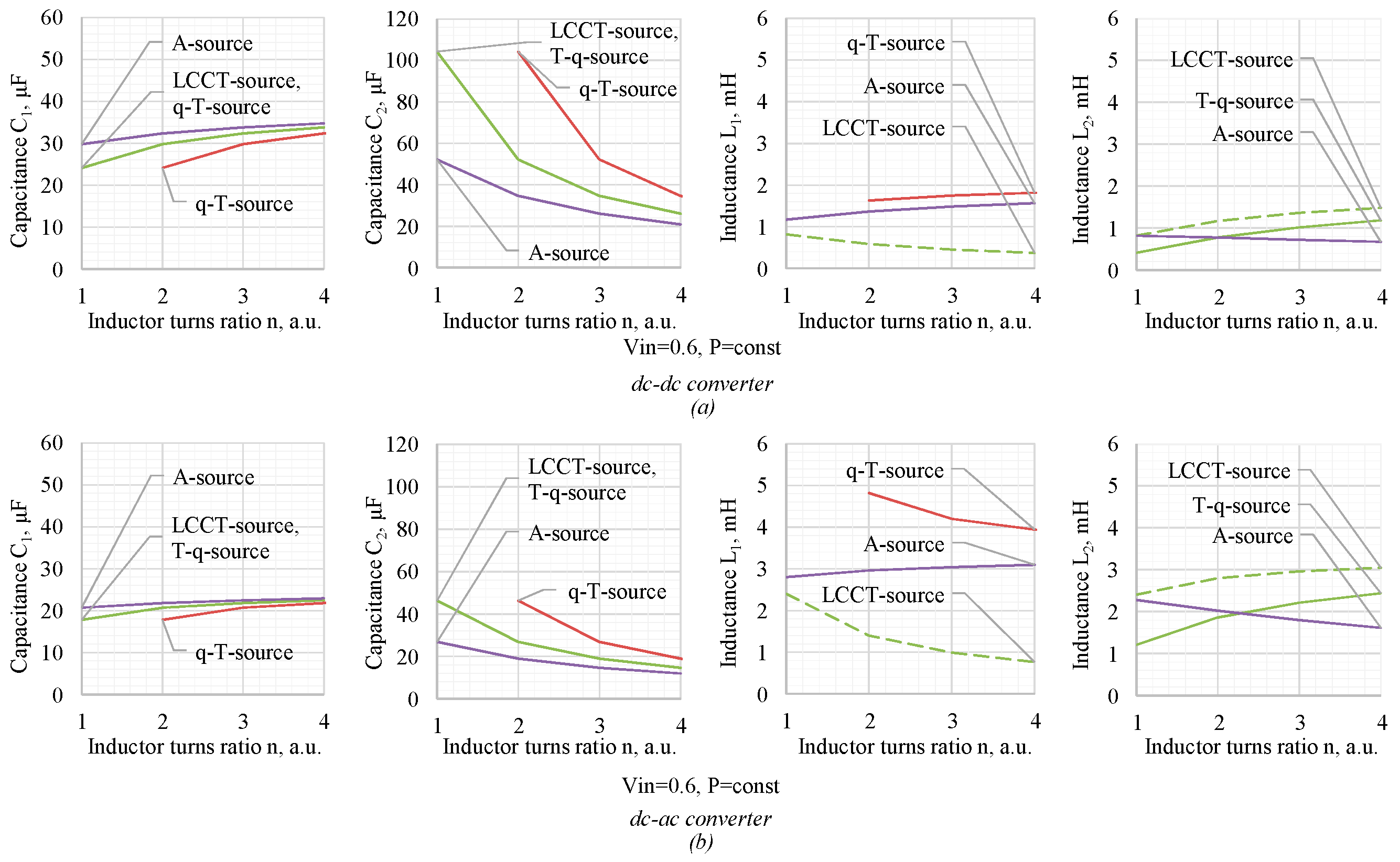
Figure 5 show the dependences of the passive elements values as a function of the input voltage and inductor turns ratio (
n), respectively.
Figure 4 shows the required values of the passive components to provide a constant current ripple in magnetic components (
L1 and
L2) and voltage ripple across the capacitors (
C1 and
C2) as a function of the input voltage.
Figure 4a illustrates the dc-dc application while
Figure 4b corresponds to the dc-ac application. It can be seen that in all cases, the increasing input voltage leads to the capacitance
C1 and inductances
L1,
L2 decreasing. This result is expected because of no need for the boosting voltage. If the input voltage corresponds to the nominal dc-link voltage, only simple VSI is enough to provide energy injection to the grid or ac load.
The most interesting conclusion is that the classical solution in the worst case (Vin = 0.4 a.u.) requires lower capacitance and inductance than all other IS solutions.
A separate study was conducted in order to verify the hypothesis that an increase in the turns ratio may improve the characteristics of the IS based converter.
Figure 5 shows that certain improvements in the value of capacitance and inductance are not evident. In particular, it can be seen that the behavior of the topologies is different, but a common conclusion is that an increase in the turns ratio leads to an opportunity to decrease one capacitor and inductance but at the same time, increasing inductance and capacitance of another one is required.
The only evident advantages of increasing the turns ratio lie in lower peak dc-link voltage for the dc-ac application.
At the same time, the value of inductance or capacitance is not an objective criterion. The value of stored energy should be analyzed. It is assumed to be proportional to the size and cost.
Figure 6 shows the maximum energy stored in the passive components during the switching period. It can be seen that in all cases, this energy is decreasing with the input voltage decreasing. If the input voltage equals the nominal dc-link voltage, the energy stored in the IS network is equal to zero. It means that no boost is required and the IS network is not required at all. A direct conclusion from this graph is that in order to provide a higher boost, the size and the volume of the passive components must be increased.
It can also be seen that the conventional solution based on the conventional boost circuit is better almost in all points. This conclusion is even more evident in the dc-ac application.
Another interesting conclusion is that high-gain IS based solutions such as the A-source network have a slightly smaller size of inductances but still higher than in the conventional solution. There is also an interesting feature of the total energy stored in capacitors in the dc-ac application: All IS based solutions have the same capacitance energy and they are independent of the turns ratio of coupled inductors. It means that different IS circuits have the same nature.
Figure 7 shows the dependence of conduction losses versus the input voltage. It is based on the assumption that conduction losses are proportional to the RMS current value in transistors and the average current in diodes. The same type of transistors and diodes were selected for all topologies (
VF = 0.8,
RDS = 0.27). It can be seen that despite a constant value of the input current, the high power losses correspond to the high boost. It means that the ST current is increasing and leads to the conduction losses increasing in semiconductors. It can also be seen that the value of the turns ratio leads to the conduction losses increasing as well. It is explained by the current ripple increasing in the semiconductors.
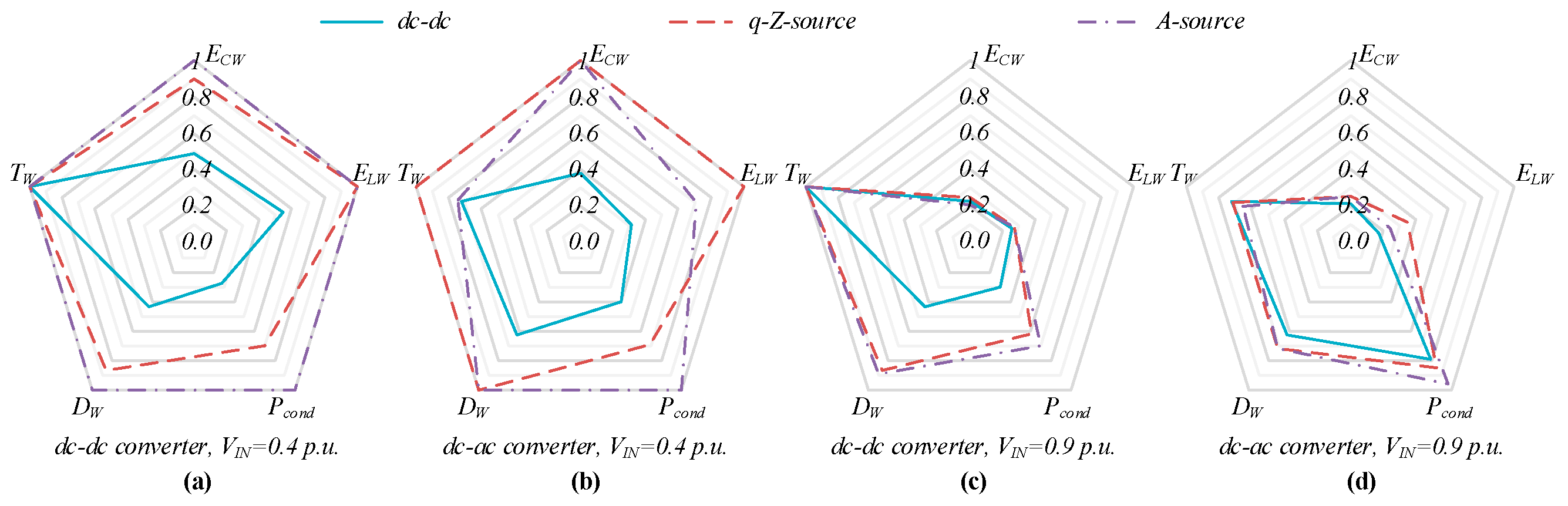
Finally, in order to summarize the results of the comparison,
Figure 8 shows several spider diagrams. These diagrams include the capacitors energy, inductors energy, voltage stress across semiconductors (diodes and transistors), and conduction losses in relative units. Among all the discussed topologies, the conventional solution with the boost circuit, the qZS network, and the A-source network were selected for the comparison. Similar to the previous figures, both dc-dc and dc-ac applications were considered.
Figure 8a shows a diagram for the dc-ac application when the input voltage is relatively low (0.4 p.u.). In this case, the size of the passive components in all IS solutions was significantly larger.
Figure 8b shows a diagram for the same input voltage but for the dc-dc application. In this case, the size of the passive components was larger as well, but the difference was not so evident.
1 p.u. of the input voltage corresponds to the boundary input voltage between the buck and the boost mode. In the case of the dc-dc converter, 1 p.u. of the input voltage is equal to the reference output voltage. All the other parameters that are shown in
Figure 8 were normalized to the maximum value.
Similar results are demonstrated in
Figure 8c,d. In this case, only a minor boost is required and the difference in the capacitors and inductors energy is not significant.
As an intermediate conclusion, it can be claimed that IS networks require larger sizes of the passive components with the same current and voltage ripples. It also means that in the case of the equal components, the ripple will be higher. Among IS network topologies, the simple qZS topology can be recommended for the dc-dc and dc-ac application. The A-source has lower inductors energy where the inductance L1 and the magnetizing inductance LM of the coupled inductor are taken into account, but also the ideal transformer should be considered. It does not contribute in terms of accumulated energy, but it contributes in terms of size and costs.
At the same time, it should be mentioned that the IS network is a more complex solution with a larger number of passive components. It gives some freedom for size components optimization. For example, the second inductor of the qZS network can be smaller at higher ripples, which does not define the input current ripple. There is also many techniques for efficiency optimization.
5. Pros and Cons for Application in Galvanically Isolated Converters
The IS technology was applied to the galvanically isolated dc-dc converter right after the introduction of the qZS network in 2009 [
2], which was the first network with a continuous input current [
6]. Later on, this research area mostly focused on high step-up dc-dc converters due to the requirements of the wide input voltage range needed in emerging applications [
30]. The basic competitor for these IS converters was CS counterparts, in particular, those with active clamping utilized, as shown in
Figure 9.
This section compares galvanically isolated qZS and CS full-bridge converters from
Figure 9. Both converters feature a capacitive filter and triangular transformer current resulting from the presence of a transformer leakage inductance in real conditions. Both of them could be controlled by means of ST generation through the overlap of active states with the cumulative ST duty cycle of
D. The qZS converter contains a higher number of passive components than that in the CS counterpart and a similar number of the semiconductor components. In such implementation, both converters will suffer from the same voltage stress of switches, but require a different ST duty cycle to achieve the required input voltage boost factor
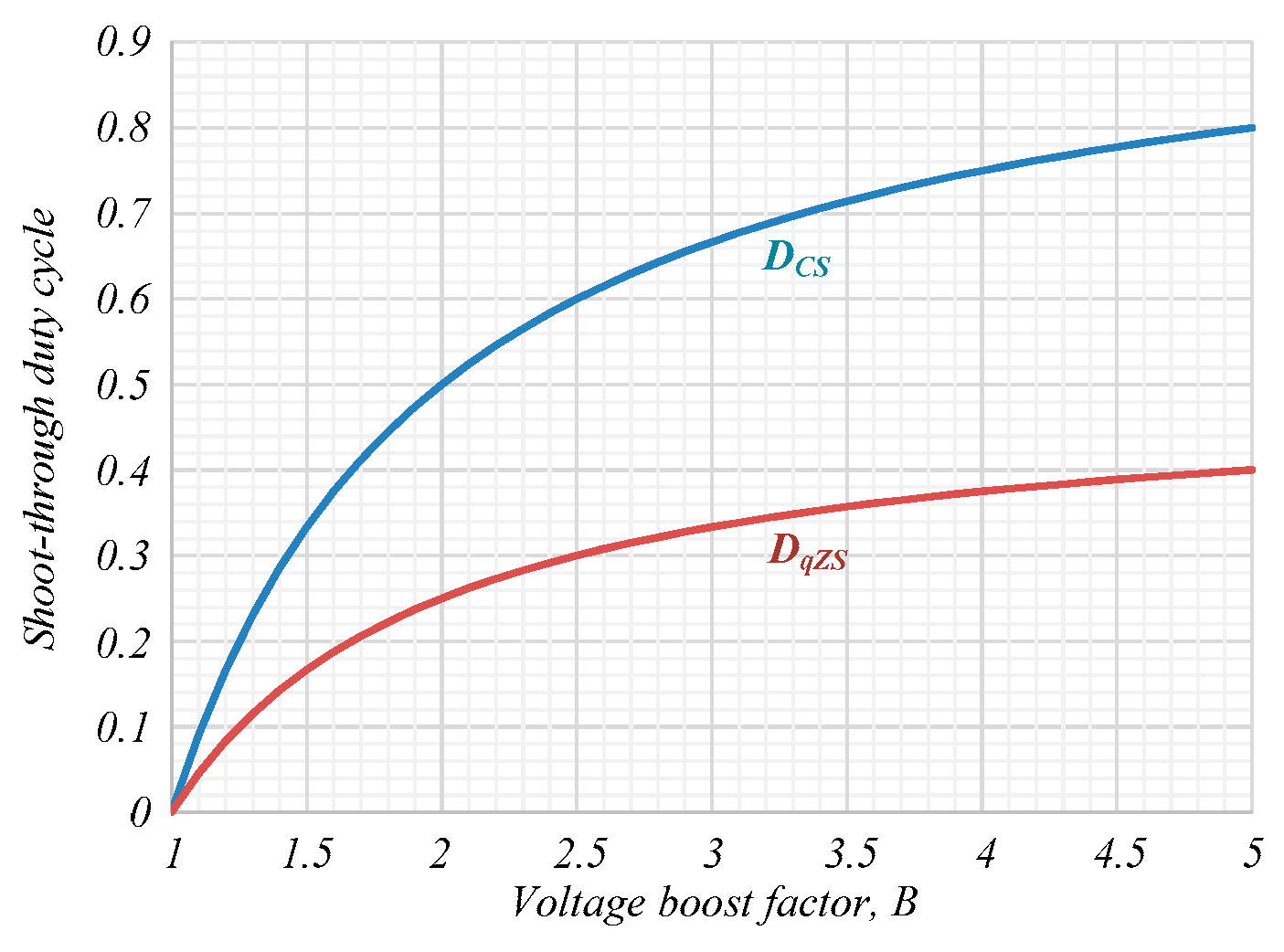
B that defines the transformer voltage amplitude. Obviously, the qZS converter requires lower duty cycle to step up the input voltage:
At the same time, the CS counterpart requires twice higher duty cycle:
Dependences (7) and (8) are visualized in
Figure 10. The curve described by Equation (7) is asymptotic to the maximum value of
DCS = 0.5, while the one of Equation (8) is asymptotic to
DCS = 1. Hence, the qZS converter provides better transformer utilization, since the active state is never less than half of the switching period: (1 −
DqZS) ≥ 0.5. Evidently, the CS converter should transfer energy through isolation within very narrow pulses at a high boost factor. As a result, the CS counterpart can suffer from a higher RMS current in the transformer as well as from a wider spectrum harmonic content of this current, resulting in higher skin and proximity losses.
Applications where the given converters compete are usually of low power at the sub-kW level. This enables implementation of the qZS network with a coupled inductor instead of the two discrete inductors. Usually, the leakage inductances
Llk1 and
Llk2 are considered to be equal. This assumption results in an ideal case, when the magnetizing current ripple is equally shared by the windings: Δ
ILqZS/2 = Δ
ILlk1 = Δ
ILlk2. However, in practice, the current ripples could be calculated as follows [
56]:
From Equations (9) and (10), it follows that the input current ripple of the qZS converter can be reduced greatly when
Llk1 ≫
Llk2. In this case, the magnetizing current ripple is distributed among the windings asymmetrically. The asymmetry is inversely proportional to the ratio of the leakage inductances, as shown in
Figure 11. In practice, the tight coupling with very low leakage inductance is relatively easy to achieve in the coupled inductor. Therefore, a small wiring inductance at the input can result in a tremendous reduction of the input current ripple. Therefore, in low power galvanically isolated applications, the coupled inductor in the qZS network could be designed to be comparable in size than the inductor of the competing CS converter. This possibility to divert the current ripple from the input source is not available in the CS converter and, hence, it gives additional flexibility over the CS counterpart.
One of the main advantages of the qZS converter is a lower RMS current of the transformer winding. The normalized value of the transformer RMS current in the qZS converter can be calculated as follows:
A similar equation could be derived for the corresponding CS converter:
Dependences (11) and (12) are compared in
Figure 12. Evidently, the RMS current stress of the transformer is up to 45% lower in the qZS converter than that in the CS converter at high boost factors.
Another advantage of the qZS converter is the lower peak current of the transformer. The normalized value of the transformer peak current in the qZS converter can be calculated as follows:
Similar to that, it can be shown that the peak transformer current of the CS converter is double of the average input current:
Dependences (13) and (14) are compared in
Figure 13. It can be appreciated from the figure that the qZS converter features up to a 70% lower transformer peak current, while the normalized transformer peak current of the CS converter is constant. It should be mentioned that these results derived under the assumption of the same current ripple in the input stage inductors.
Operation of the qZS converter with lower ST duty cycles is associated with twice higher current stress during the ST states in the inverter bridge. As a result, the normalized RMS switch current of the qZS converter is calculated as:
is higher than that of the CS converter calculated as:
which results in increased RMS losses in the qZS converter, as shown in
Figure 14. Moreover, this stress is the same for both topologies at the low boost factors up to 1.7, while the gap increases to up to only 15% at very high boost factors. Hence, this small increase in the current stress of the switches is not a challenge in low power high step-up systems, where low voltage Si MOSFETs with very low on-state resistance are commonly utilized.
Another disadvantage of the qZS converters that becomes apparent as compared to the CS counterparts is the higher flux density swing in the transformer resulting from a longer active state of the qZS converter. The core flux swing Δ
BS is proportional to the transformer voltage and the duty cycle: Δ
BS ∝
B·
Vin·(1 −
D). This results in up to a three times higher core flux density swing, as shown in
Figure 15. This implies that the transformer should be designed differently for the qZS and CS converters.
From the considerations described above it follows that IS converters optimize the operation of the magnetic components, take advantage of wiring inductance to achieve ripple-free input current, and provide buck regulation mode, considerably enhancing the input voltage regulation range—all of these features are unavailable in the CS converters. However, design of the IS converters is more complicated due to the design constraints described above.
6. Simulation and Experimental Study
In order to verify the theoretical conclusions, a simulation and an experimental study were performed. The qZS and A-source networks were selected for practical realization as the most evident representatives of the discussed network topologies. The parameters of the selected topologies are presented in
Table 2. A three-phase dc-ac system was selected for simulation and experimental verification.
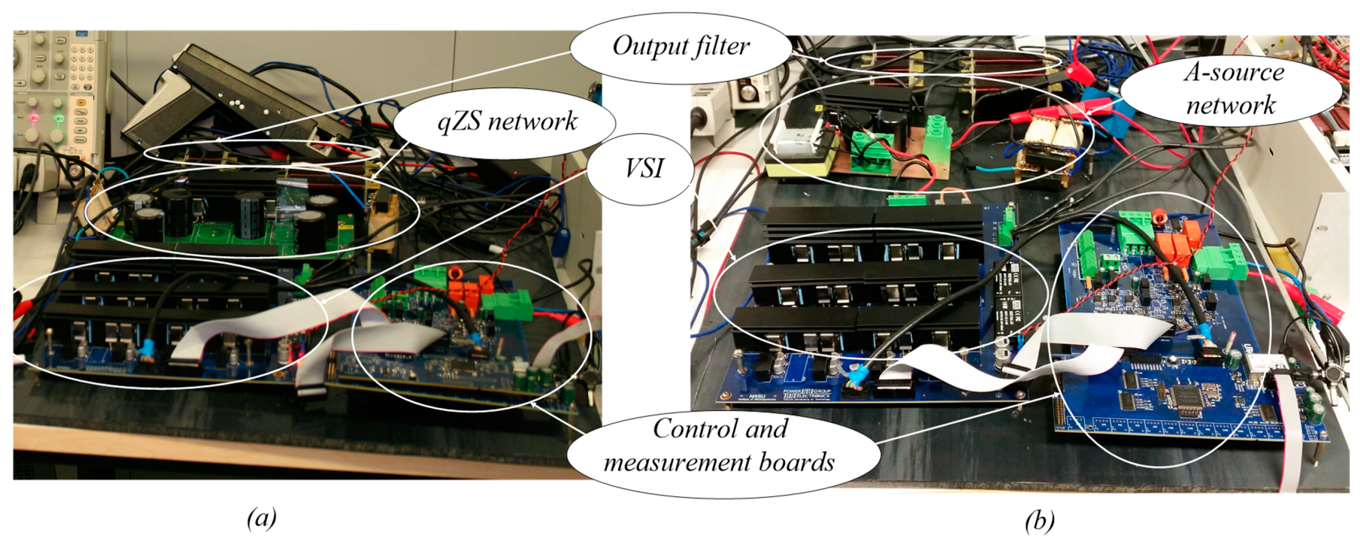
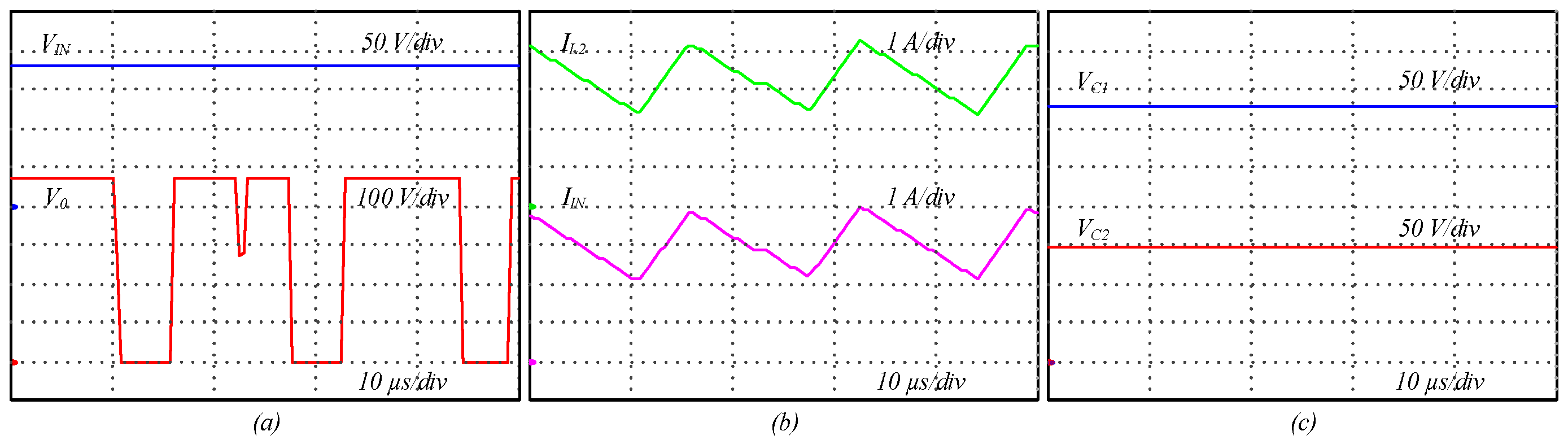
Figure 16 shows the experimental setup. It consisted of the three-phase VSI, qZS or A-source network, and inductive output filter. The control board was based on a field-programmable gate array (FPGA) which is able to provide any modulation technique. The measurement system was also involved for general monitoring. The experimental setup depicted in
Figure 16a belonged to a qZS inverter, while the setup depicted in
Figure 16b belonged to an A-source inverter. It can be seen, that it is the same setup and only IS networks were replaced.
Selected topologies were compared by the same parameters of the input voltage, load, capacitors, and input inductor value. The input voltage was equal to 183 V with a RMS ac output voltage of about 110 V.
Figure 17 shows the simulation results for the qZS network, while
Figure 18 shows similar results for the A-source network. It can be seen that approximately the same output voltage was achieved for different circuits. The ST duty cycle
DqZS = 0.2 of the A-source was smaller than
DqZS = 0.27 of the qZS.
The input current quality of the A-source was slightly better. The input average current value of the A-source was lower than qZS: The average value of the input current was Iin = 2.6 A and Iin = 3.14 A, respectively.
However, it can be seen that the capacitor voltages of the A-source were almost the same as the capacitor voltages of qZS: The average value of VC1 = 307 V, VC2 = 128 V and VC1 = 342 V, VC2 = 156 V, respectively. Generally, the above confirms the theoretical results. The average value of the transformer current was approximately zero. This indicates that the transformer core was not saturated.
In order to finalize the verification,
Figure 19 and
Figure 20 show the experimental results that fully corresponded to the simulation results.
Figure 19 illustrates the experimental results of the qZS circuit board. At the same time,
Figure 20 shows the obtained results of the A-source circuit board.
Finally, all the results are summarized in
Table 2. Except for simulation and experimental verification, the theoretical results are represented.
It can be seen that circuits were tested under different power levels, which is due to the limited power of the transformer of the A-source network, but the main idea of the simulation and the experimental study was to confirm the feasibility of the derived equations in
Table 1. It has very good coincidence with the simulation results. It means that previously shown diagrams based on the same approach are valid as well. Minor differences between the simulation and the experimental results can be explained by the tolerance of the passive components and losses in the power conversion.
Table 2 also has parameters of the passive components including maximum stored energy according to the specification and actual size of the element.
Except for typical values of the passive components, voltage, and current across passive elements,
Table 2 shows the size of the passive elements and energy that could be stored in them. First of all, it can be concluded that the size of the passive elements is proportional to the energy and the assumption described above is correct. Secondly, it was also obvious that some of the passive components are overdesigned. They were chosen for the experimental setup just because of their availability in the lab. At the same time, in order to demonstrate a more objective value of energy, real voltage across the capacitors and the inductors current were taken into account.
It clearly showed that required energy was stored in the passive element in a certain operation point. The obvious conclusion that the A-source inverter may require a slightly smaller overall inductor’s size as compared to the qZS solution, but the transformer has to be taken into account as well.
Despite the different power level, it could be seen that experimentally obtained values were correlating with those theoretically estimated in
Figure 8. The capacitance energy was almost the same while the inductance energy was smaller in the A-source network. At the same time, the additional transformer, the size of which is significant, was used in the A-source network. The instantiations value of the energy stored in the transformer was zero, but the size and cost should be taken into account.
7. Conclusions
IS networks are popular in the research area, in particular in a single-stage buck-boost dc-dc and dc-ac applications.
This paper presented a comprehensive analytical and experimental comparison of the IS-based buck-boost solutions in terms of the passive components and semiconductors.
The main criterion for this comparison was the stored energy in the passive elements, which was considered under a constant and predefined high frequency current ripple in the inductors and the voltage ripple across the capacitors. Semiconductor stress and the range of input voltage variation were considered as well. First of all, it was clearly demonstrated that in order to provide higher boost of the input voltage with the same ripples, much larger passive components are required for any solution. Secondly, almost in any case, the classical solution requires lower capacitance and inductance than all other IS solutions.
Also, an interesting conclusion is that the overall size of the similar IS based converters designed for identical operating conditions is the same. Some differences can be obtained for high boost IS solutions. Most of them are based on the coupled inductor or transformer, which in turn adds some volume and cost.
The main drawback of any IS based inverter lies in the increased voltage stress across semiconductors. A high-voltage gain solution may mitigate this drawback, but such solutions demand additional magnetics.
It should also be mentioned that the calculation approach of the proposed passive components was very simplified. In practical experience, some of the capacitors or inductors can be smaller or with an increased ripple. Different optimization techniques can be applied. The most evident advantages of IS networks application correspond to the galvanically isolated converters. It consists in the magnetic components optimization.


 ,
, 


