Article

Common Switch Fault Diagnosis for Two-Stage DC-DC Converters Used in Energy Harvesting Applications

1
ECAM Strasbourg Europe—ICube Laboratory UMR7357, 67400 Illkirch-Graffenstaden, France
2
Institut Jean Lamour (UMR7198), Université de Lorraine, 54000 Nancy, France
3
GREEN Laboratory, Université de Lorraine, 54000 Nancy, France
*
Author to whom correspondence should be addressed.
Electronics 2019, 8(3), 293; https://doi.org/10.3390/electronics8030293
Submission received: 30 January 2019 / Revised: 19 February 2019 / Accepted: 25 February 2019 / Published: 5 March 2019

Abstract

:
This paper proposes a new Unified Switch Fault Diagnosis (UFD) approach for two-stage non-isolated DC-DC converters used in energy harvesting applications. The proposed UFD is compared with a switch fault diagnosis consisting of two separate fault detection algorithms, working in parallel for each converter. The proposed UFD is simpler than the two parallel fault diagnosis methods in realization. Moreover, it can detect both types of switch failures, open circuit and short circuit switch faults. It can also be used for any two-stage non-isolated DC-DC converters based on two single switch converters, no matter the converter circuits in each stage. Some selected simulation and Hardware-in-the-Loop (HIL) experimentation results confirm the validity and efficiency of the proposed UFD. Also, the proposed UFD is applied successfully for fault-tolerant operation of a buck/buck–boost two-stage converter with synchronous control and a redundant switch.

1. Introduction

Because of the global problems of energy shortage and the impact of energy resources (coal, oil, and natural gas) on our environment, energy harvesting techniques have become one of the most interesting research areas [1,2]. By these techniques of energy harvesting, environmental energy can be extracted and converted into the desired form of energy for different applications [3].
On the other hand, the fast development of wireless technology and micro-electromechanical systems (MEMS) offers many portable low-power applications that could be widely used in daily life. Considering the limited lifetime of batteries and challenges of battery replacement (recharging), self-powered applications using ambient energy harvesting have been studied in recent years [4,5]. Some examples of energy sources suitable for energy harvesting are solar, vibration, thermal, and bio-fuel sources. These energies can replace batteries to provide longer operation lifetime without the need for battery replacement under stringent situations [3]. For example, new implantable biosensors that are miniaturized in size and power consumption can be powered by an energy harvesting solution to avoid battery replacement [4].
One of the most promising thermal energy harvesting DC sources is the thermoelectric generator (TEG). TEG devices can directly convert thermal energy into electricity without any moving parts. Thanks to the advantages of TEG, like light weight, no noise and no mechanical vibration, TEGs could be a suitable solution for many applications where a temperature difference (ΔT) exists, such as human bodies, plants, automobiles, and so on [1,2,4,6].
Photovoltaic (PV) energy is also one of the most popular DC renewable energy sources for an energy harvesting system with a compound annual growth rate of 42% from 2000 to 2015 [7]. PV energy has been used recently in some applications, such as manned [8,9] and unmanned vehicles [10,11] and wearable technology [12,13].
Due to the intermittent and unregulated nature of the previously discussed energy resources (TEG and PV), Maximum Power Point Tracking (MPPT) algorithms must be employed to maximize the power transfer from the source to the load. The MPPT algorithm must be implemented in the first stage of the energy conversion chain. Moreover, in many applications, the output voltage level of the energy harvesting system must be controlled and adapted to the load voltage. The best choices to apply these algorithms (and control), undoubtedly are two-stage DC-DC converters [7,14,15,16].
Thus, different types of DC-DC converters have an important role in renewable energy resources and energy harvesting applications. Generally, there are two different categories of DC-DC converters: Isolated and non-isolated. In isolated converters, transformers are used to provide the desired output voltage according to load requirements. For the non-isolated DC-DC converters, no transformer is used, therefore, these converters are preferred in energy harvesting applications because of lower cost, higher efficiency, smaller volume, and simpler topology [17], compared to isolated ones.
Continuity of service and electrical power availability for applications such as medical devices, embedded systems, or sensor networks supplied by energy harvesting systems, has become mandatory [18]. The continuity of service can be affected by a failure. A failure is defined as an unpermitted deviation of at least one characteristic property or parameter of a system from the acceptable/usual/standard condition [19]. In any case, the failure of a single component may cause the dysfunction and shutdown of the entire system. Therefore, to avoid further damages after an occurrence of failure and to perform service continuity, fault-tolerant capability is required. This paper focuses on the diagnosis of switch failures in DC-DC converters used in energy harvesting systems, that is mandatory for further fault-tolerant purposes.
Particularly, in this paper, a unified approach for switch fault diagnosis is proposed using two-stage non-isolated DC-DC converters with fault-tolerant capabilities, supplied by a renewable DC source, such as TEG and/or PV.
In the following section, the classical DC-DC converters are discussed. In Section 3, the general principle of switch fault detection in two-stage converters is first introduced. Then, two-fault detection approaches are detailed in the case of the two-stage DC-DC converter, based on parallel Fault Detection (FD) and on the proposed Unified Switch Fault Diagnosis (UFD). Finally, both of them are compared at the end of the section. Selected simulation results are presented and discussed in Section 4. In Section 5, the principle of an experiment based on Hardware-in-the-Loop (HIL) is first explained and then applied to the case of a two-stage buck/buck–boost converter with fault-tolerant capability, based on synchronous control and a redundant switch. Both simulations and HIL results confirm the validity and effectiveness of the proposed UFD. Thanks to the FPGA implementation and algorithm performances, the fault can be detected in less than one switching period.

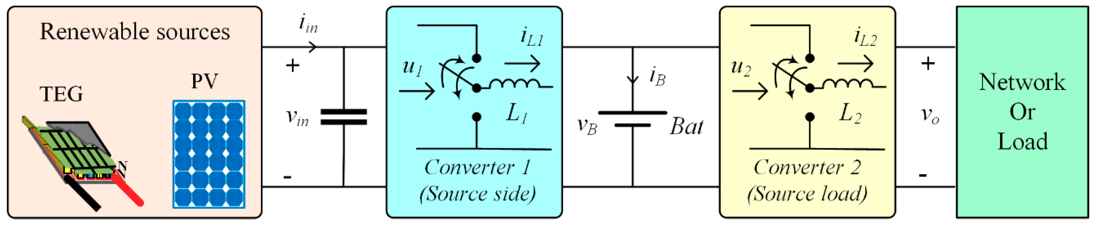
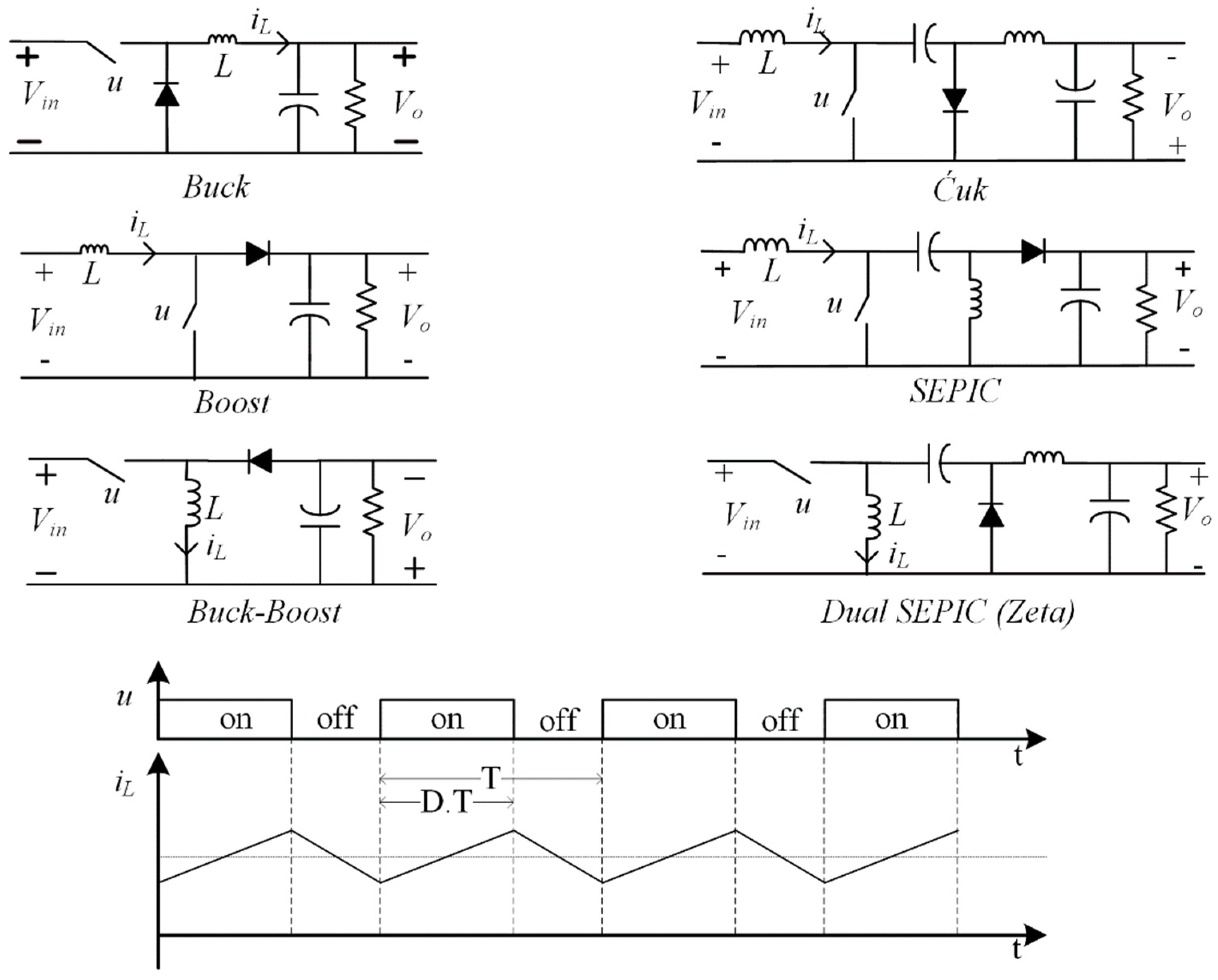
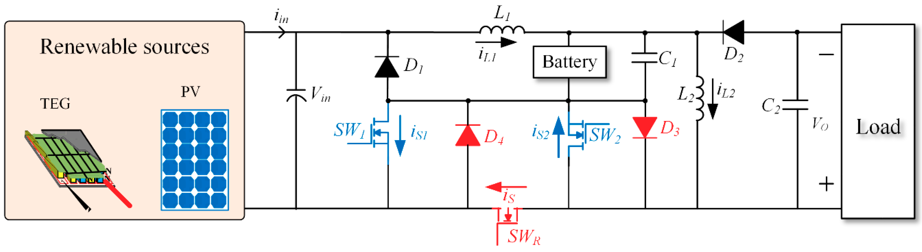
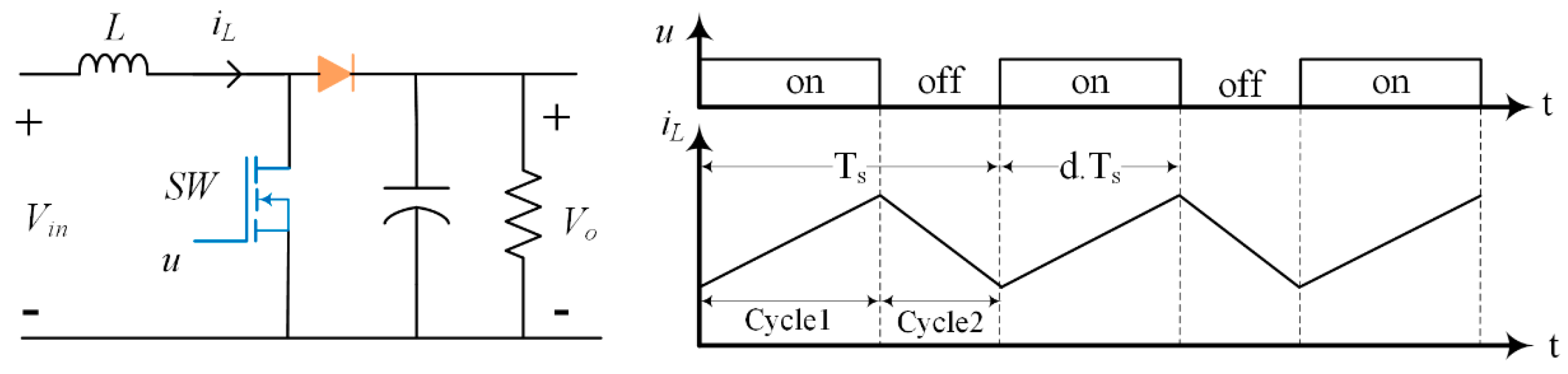
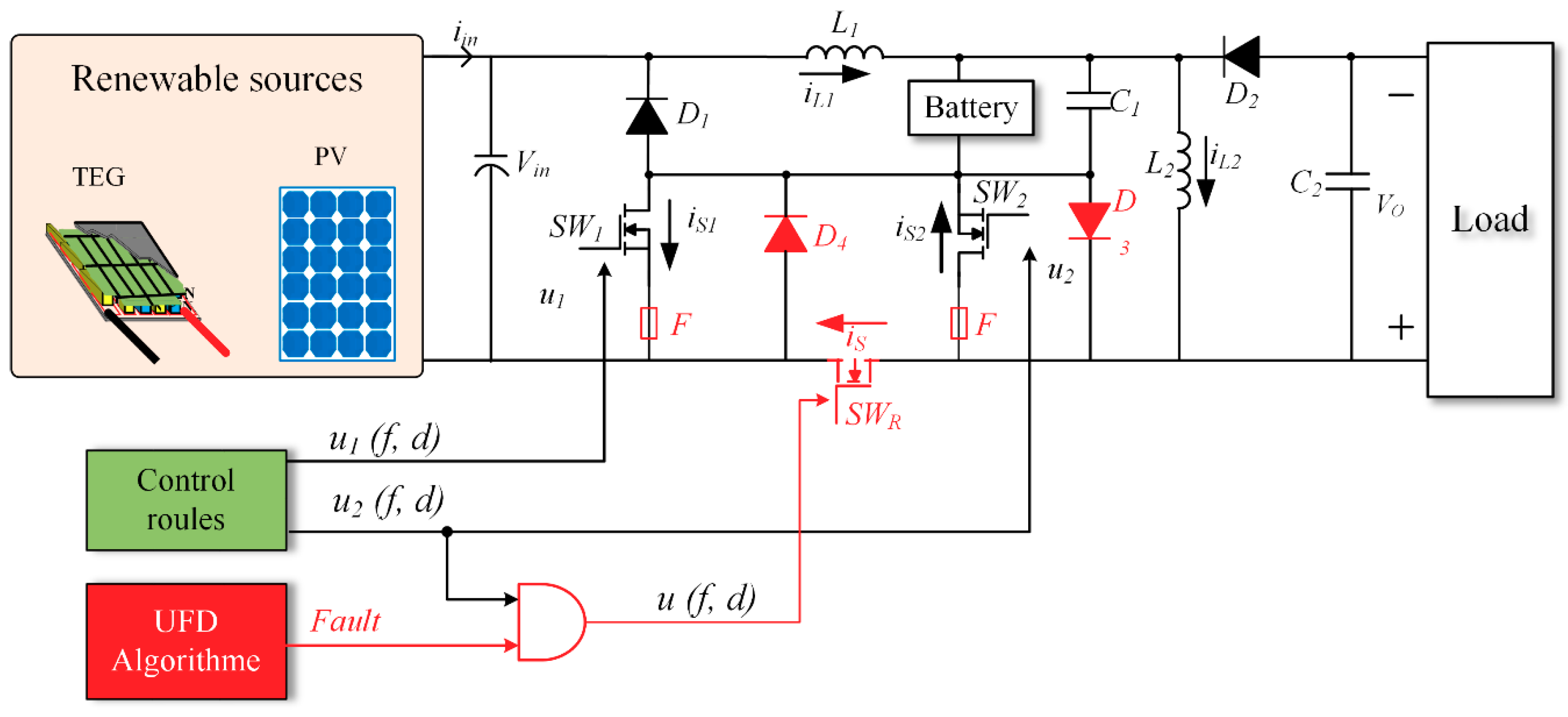
2. Classical Two-Stage DC-DC Converters

Classical two-stage non-isolated DC-DC converters used in an energy harvesting system (with photovoltaic or TEG source) are illustrated in Figure 1. They consist of two cascaded non-isolated single switch converters. Generally, in such systems, the source side converter realizes the Maximum Power Point Tracking (MPPT). At the load side, the second converter controls the output voltage level, also providing a step-up or step-down output voltage level, according to load side requirements [20].
The converters in each of the two stages can be one of the single switch converters such as buck, boost, buck–boost, Ćuk, SEPIC, or dual SEPIC, as shown in Figure 2. In this family of converters, the shape of the current “iL” that passes through the inductor directly connected to the switch is the same [21]. The proposed UFD algorithm is based on the observation of this inductor current shape’s similarity and it can be applied to both stages of a cascaded non-isolated DC-DC circuit, regardless of the converter type (step-up and/or step-down).

3. Switch Fault Diagnosis

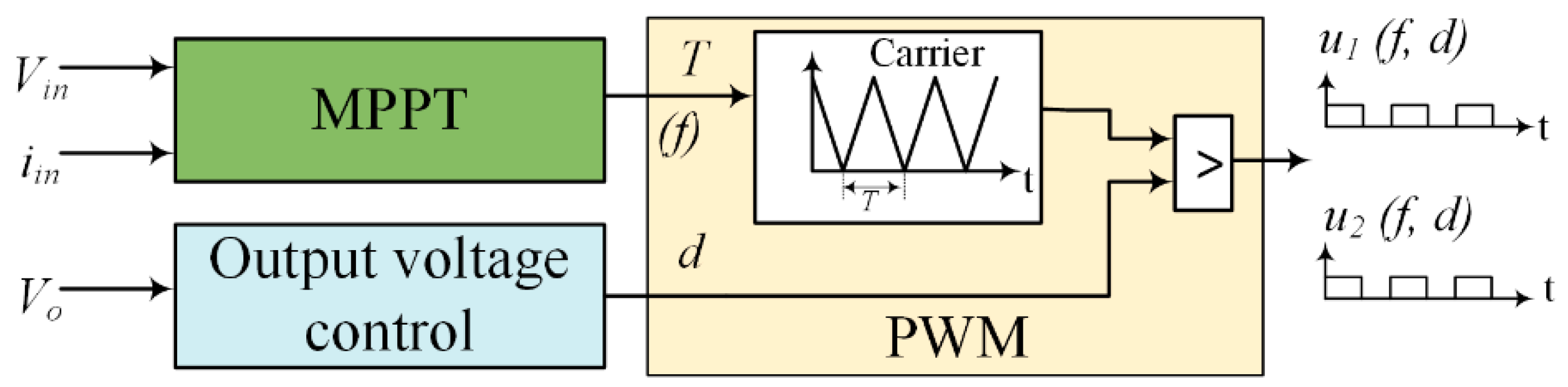
3.1. General Principle of Switch Fault Detection

In power electronics (and electronic) converters, semiconductor switches are one of the most fragile elements, and they have caused 21% of total failures [21] in different applications. Thus, due to the high shutdown cost and the safety aspect of energy harvesting and renewable energy applications, consisting of electronic converters, the reliability of these systems is a significant challenge. That is why the fault diagnosis and the fault-tolerant operation of electronic converters in order to increase reliability, perform service continuity of the systems, and reduce high maintenance costs has become one of the most interesting topics for researchers in recent years [17,19,21,23,24,25].
The most common failures in switches are open-circuit faults (OCF) and short-circuit faults (SCF). These failures may happen mainly due to incorrect gate voltage, driver failure, or rupture of the switch (which can be a consequence of an SCF, as explained later) [26,27]. Indeed, in practice, an OCF may be a consequence of a gating fault or an SCF. In the second case (SCF), a fast fuse is usually connected in series with the switch of the fault-tolerant converter, as proposed in [27]. Thus, an SCF will become an OCF (from an electrical circuit point of view) after the fuse break. Therefore, in this paper, both OCF and SCF are concerned.
In the general case, switch fault tolerance in electronic converters requires three consecutive steps: Fault diagnosis, fault identification, and remedial actions. The contribution of this paper focuses on the first step—the fault detection. Nevertheless, to validate the proposed UFD, it is applied to a fault-tolerant two-stage DC-DC converter, here, the buck/buck–boost two-stage converter studied by Siouane et al. [28]. Furthermore, the fault operation was also verified, based on the proposed UFD. Nevertheless, the proposed UFD remains suitable for any type of two-stage non-isolated DC-DC converter.
Switch fault diagnosis for single-switch non-isolated DC-DC converters and fault-tolerant converters have been studied and published [21,22,26,27,29,30,31,32]. In these papers, observation of the inductor current shape according to the switching pattern is the base of all the proposed FD methods. Moreover, only a few papers have proposed remedial actions and fault-tolerant circuits for two-stage DC-DC converters [28]. In [28], a fault-tolerant cascaded buck/buck–boost converter with energy storage was recently examined under synchronous control, but fault detection was not discussed.
Siouane et al. proposed in [25] a fault-tolerant DC-DC circuit, shown in Figure 3. According to this topology, the switch fault location is not necessary for post-fault actions. In this condition, using two separate fault detection algorithms with fault localization capability, which is certainly efficient, neither were optimized nor useful. Indeed, as detailed in [25], regardless of the detected switch in OCF case, both switches used in healthy conditions (the blue ones SW1 and SW2 in Figure 3) were controlled to be opened before applying remedial actions. Then, a shared redundant switch (SWR in Figure 3) associated with the two diodes D3 and D4 replaced these two switches SW1 and SW2. After this remedial action, the post-fault operation was done by applying a new synchronous control system to the redundant switch SWR (the red one) [28].

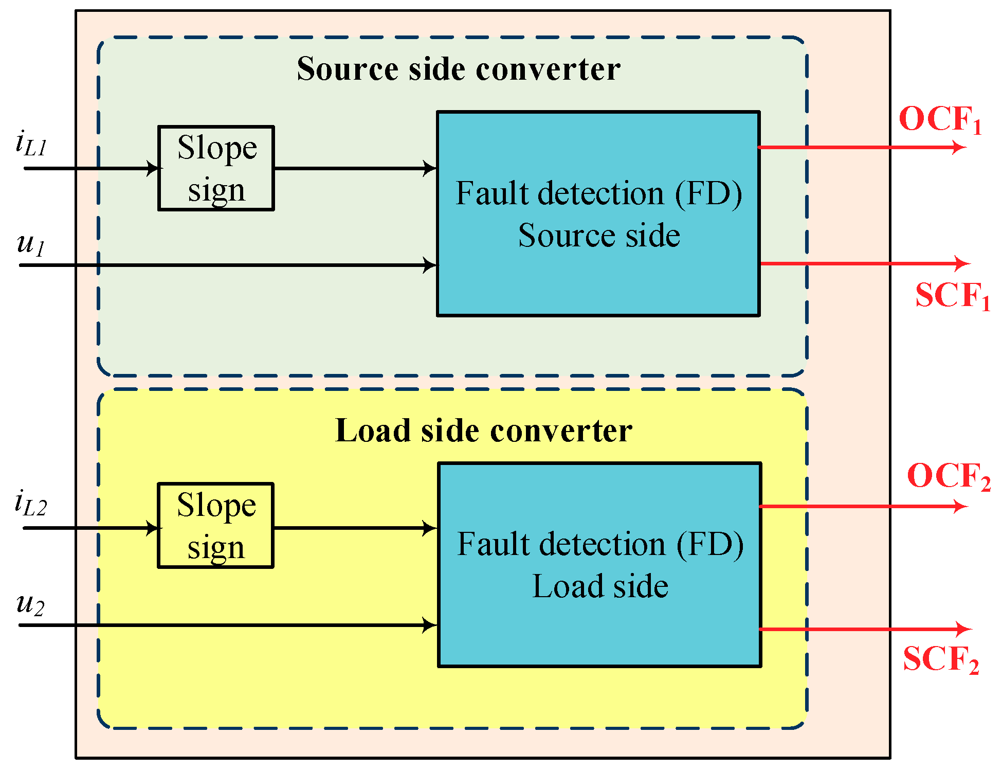
3.2. Parallel FD Algorithms

In this section, we consider the case of parallel FD. In this method, two identical FD algorithms (one algorithm for each converter) are working together, as illustrated in Figure 4 where u1 and u2 are the switching patterns, applied to SW1 and SW2, respectively. For each FD block in Figure 4, one of the proposed methods in [21,27] could be used, which are based on the observation of the inductor current shape.
As is illustrated in Figure 2, the inductor currents in non-isolated single switch converters are similar. Therefore, these FD methods can be applied in both converters (source side or load side) of a cascaded non-isolated converter, presented in Figure 1. In Figure 4, OCF1 and SCF1 declare open circuit and short circuit faults, respectively, for the source side converter. The OCF2 and SCF2 are dedicated to failure detection on the load side converter for open circuit and short circuit faults, respectively.
Figure 5 shows a boost converter, its switching pattern signal (u), and inductor current iL(t). According to Figure 5, one switching period (Ts) consists of two cycles of converter operation: Switch SW on (Cycle 1) and switch SW off (Cycle 2). As Figure 5 illustrates, when the switch is on, the inductor current (iL) increases and when the switch is off, it decreases. A failure is declared if iL increases or decreases for more than one switching period.
As detailed in [21,27], a state machine (SM) is used to realize the FD algorithm in each of the FD blocks of Figure 4. After a switch fault occurrence, according to the localization of the failure (source side or load side converter), one of the FD blocks is declared the fault. As a result, one of the output signals (OCF1, SCF1, OCF2 or SCF2) would be set to “1”, depending on the fault type in one or two switching periods. Therefore, by applying the parallel FD algorithm beside fault detection, fault identification (OCF or SCF) and localization can be provided. As discussed in [18], to perform service continuity for a two-stage non-isolated DC-DC converter (Figure 3), the fault detection is mandatory. Fault identification and localization are not necessary because, after a fault occurrence in one of the two stages, reconfiguration and post-fault operation are the same.

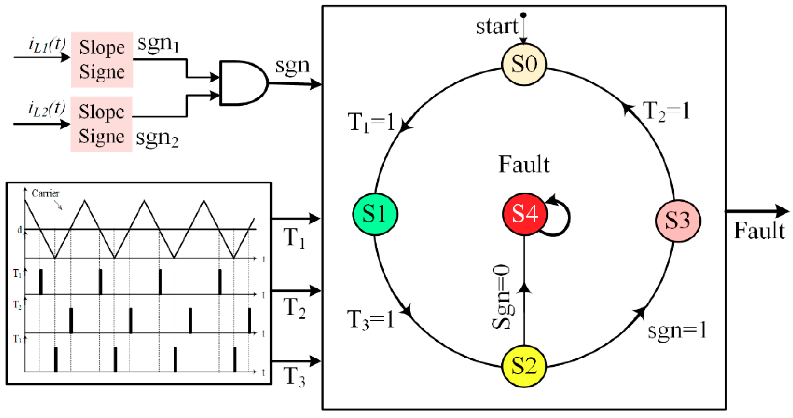
3.3. Unified Fault Diagnosis (UFD) Algorithm

The idea of a common switch fault diagnosis for two-stage DC-DC converters was first introduced in a conference paper [33]. Nevertheless, the fault detection approach was not presented as a result of the general approach for designing unified fault detection (UFD). Moreover, in [33], the detection was not applied to a fault-tolerant two-stage converter (here a fault-tolerant buck/buck–boost with a synchronous redundant switch) and validated by HIL experiments, from the fault detection to the post fault operation of the converter.
A so-called UFD method is presented here for a cascaded non-isolated DC-DC converter under synchronous control. It means that both of the converters are controlled by two identical switching patterns, (u1(f, d) and u2(f, d)), that are produced by using a single carrier signal, as it is illustrated in Figure 6. Generally, the frequency f of the carrier is imposed by the MPPT algorithm (source side converter) and the duty cycle d is determined according to the required output voltage level (load side converter). This paper is focused on the switch fault detection method. More details about the synchronous control of the cascaded non-isolated DC-DC converter can be read in [25].
The proposed UFD observes u, which is defined as follows:
u = u 1   &   u 2
The proposed UFD method is also based on the same theory as the parallel one: When the switches are on, both inductor currents (iL1 and iL2) increase and when they are off, the inductor currents decrease.
To realize the proposed UFD method, a state machine (SM) is used. The SM consists of 4 inputs, 5 states, and 1 output, as shown in Figure 7. Figure 8 shows the signals and states of the SM during normal and faulty conditions.
According to Figure 8, T1 and T2 correspond to rising edges (switch on) and falling edges (switch off) for the switching pattern, respectively. The T3 signal is activated in the middle of Cycle 1, which permits checking the health of the switches when they should be in the “on” state. The signs (not the exact values) of the inductor current slopes (sgn1 and sgn2) are needed for this algorithm. To obtain these signals, the value of the inductor current is compared with its value at Tsgn = 4Ts beforehand (Ts is the sampling period). It is equal to “1” when the switch is on (current increases) and it is equal to “0” when the switch is off (current decreases):
s g n 1 = { 1 , i f   i L 1 ( t ) i L 1 ( t 4 T s ) > 0 0 , i f   i L 1 ( t ) i L 1 ( t 4 T s ) < 0
s g n 2 = { 1 , i f   i L 2 ( t ) i L 2 ( t 4 T s ) > 0 0 , i f   i L 2 ( t ) i L 2 ( t 4 T s ) < 0
Under synchronous control, both currents increase and decrease simultaneously in one switching period. Therefore, if one of the inductor currents (iL1 or iL2) is always increasing or decreasing over a switching period, it means that a failure has occurred. In this UFD, to verify this principle rule, the UFD observes sgn signal that is defined as follows:
s g n = s g n 1   &   s g n 2
Thus, as illustrated in Figure 7 and Figure 8:
  • In normal operation mode of the converters and for each period, SM starts from the initial state (S0) and the transitions occur successfully towards the state S3, consecutively (S0→S1 →S2→S3→S0);
    When the switching commands are activated, T1 goes to “1”, then a transition occurs from S0 to S1;
    The SM stays in S1 until the middle of the period during which the switches are on. When T3 is set to “1”, the SM goes to S2;
    In S2 the SM checks the state of the switches, to be sure they are closed (on). If the sgn is equal to “1”, it means that the switches operate correctly, and the SM goes to S3;
    At falling edges of the switching patterns, the switches go to “off” situation. At this time, T2 is set up to “1”, and then a transition to S0 occurs;
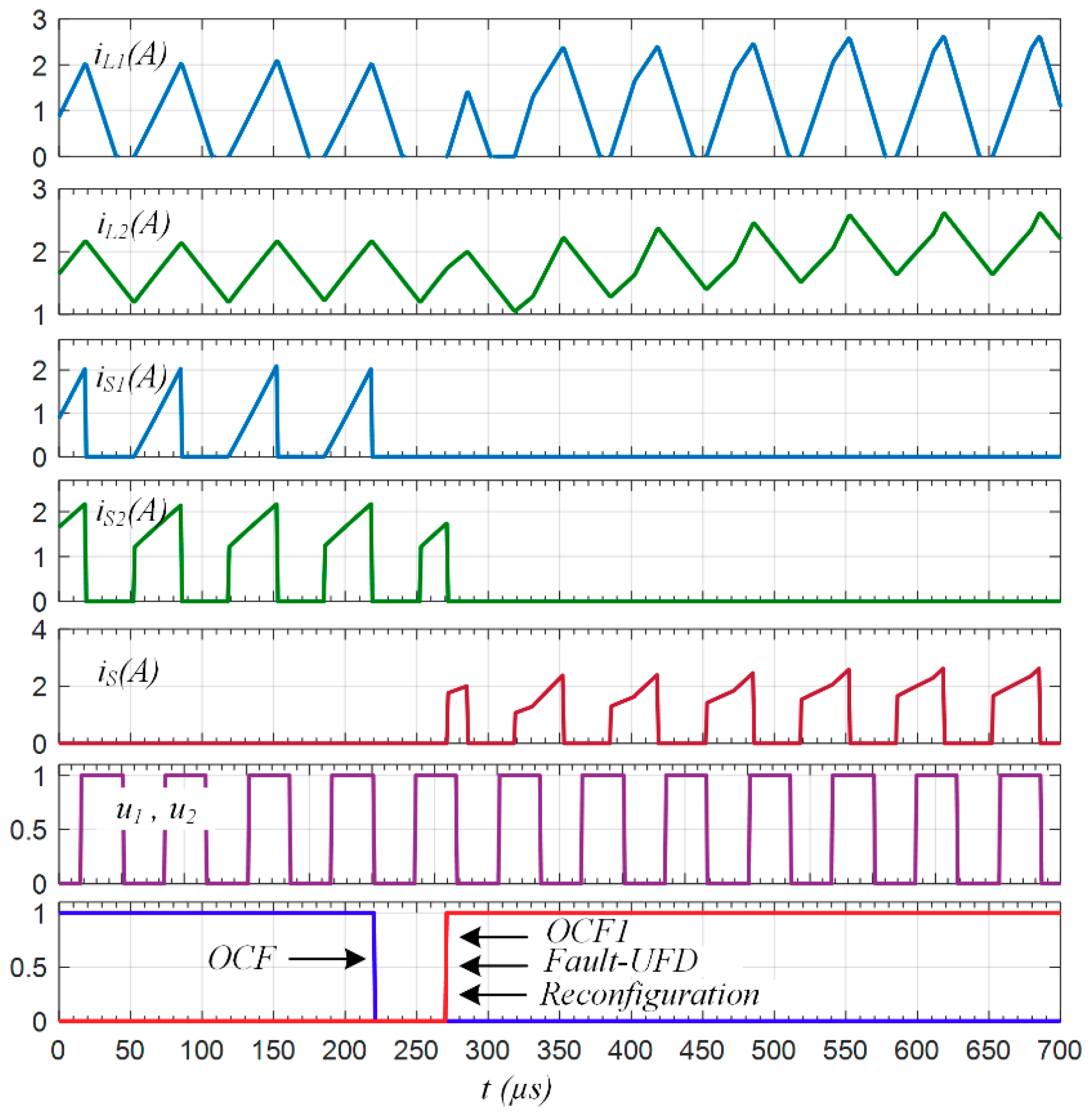
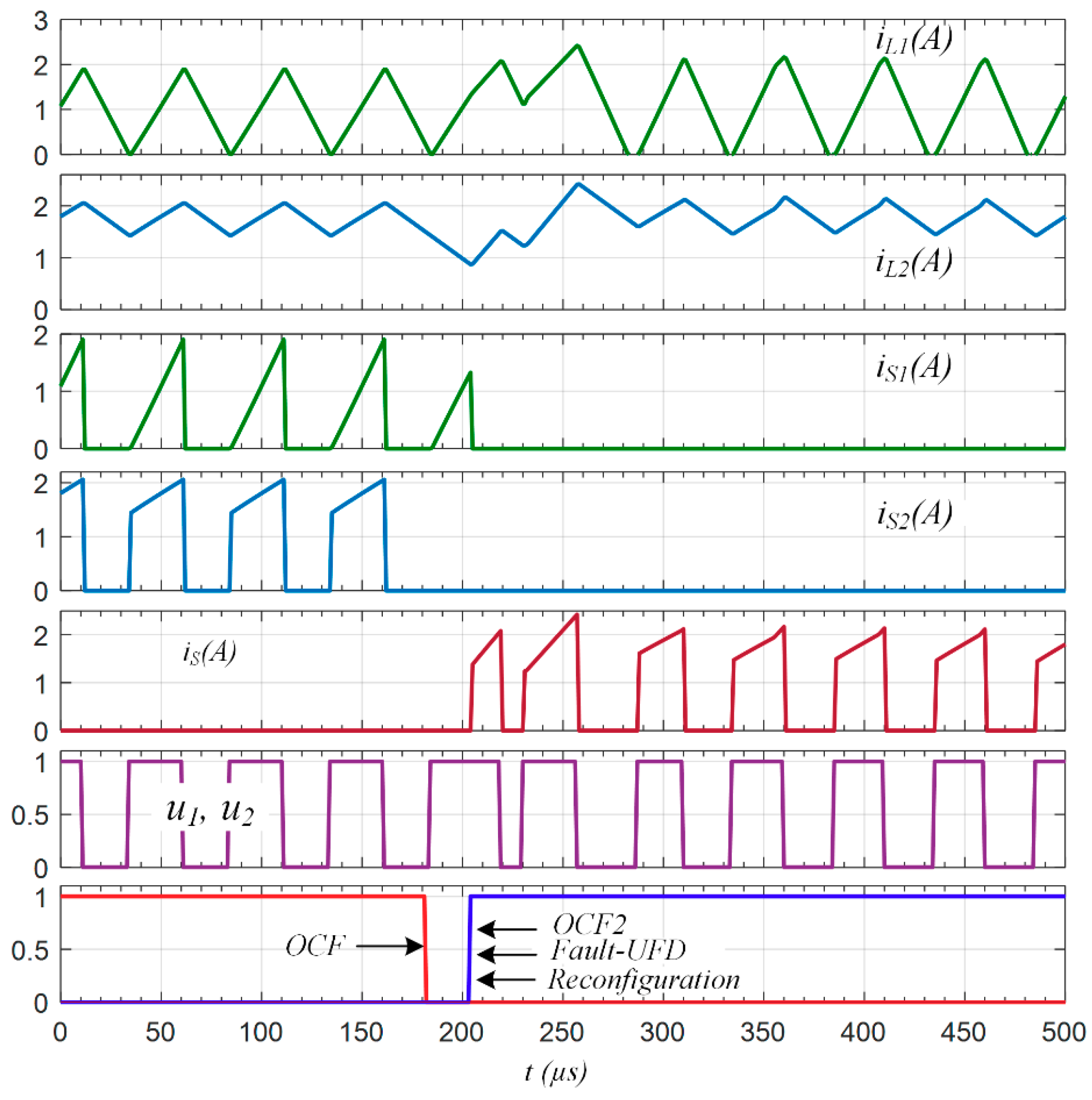
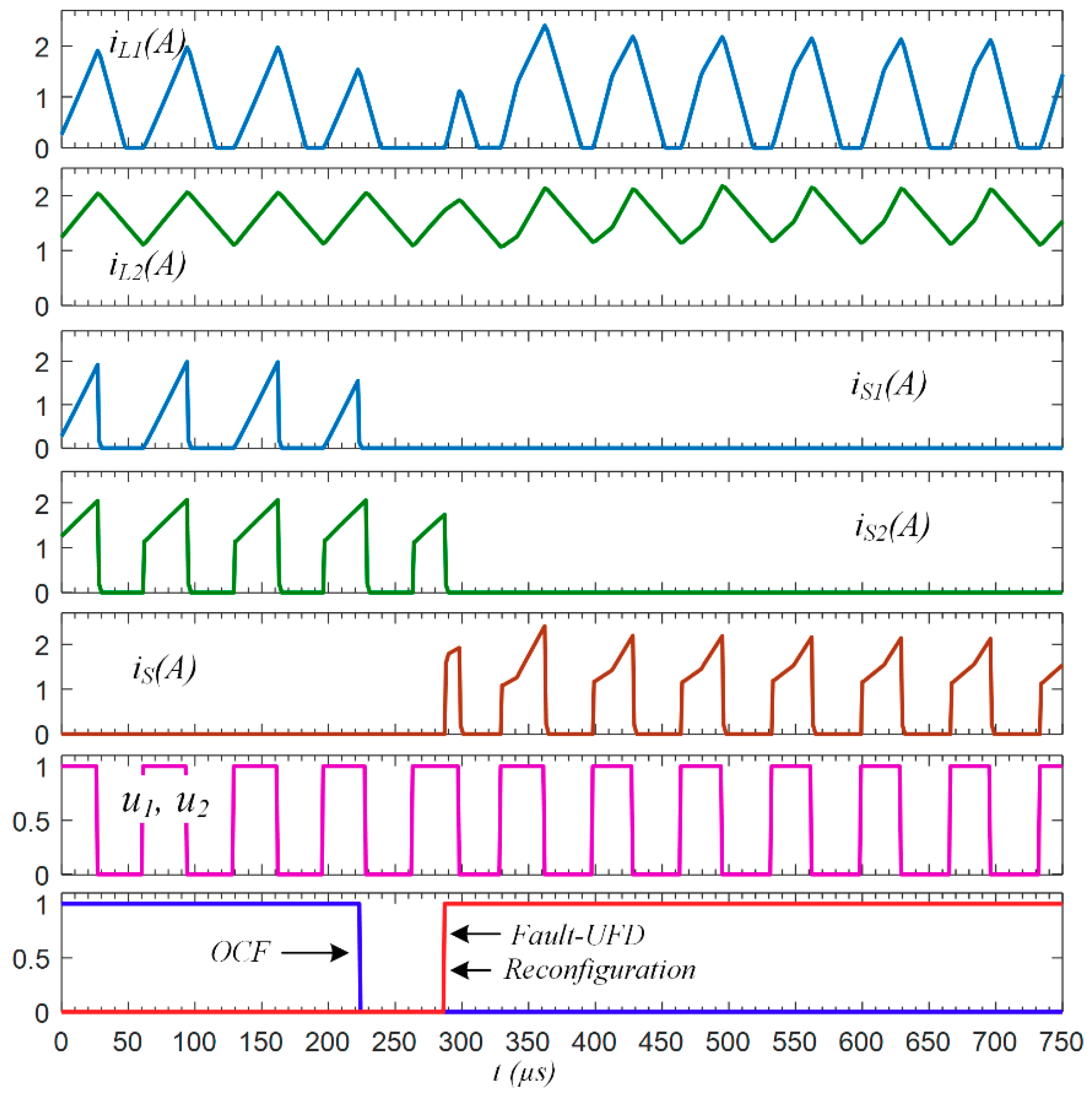
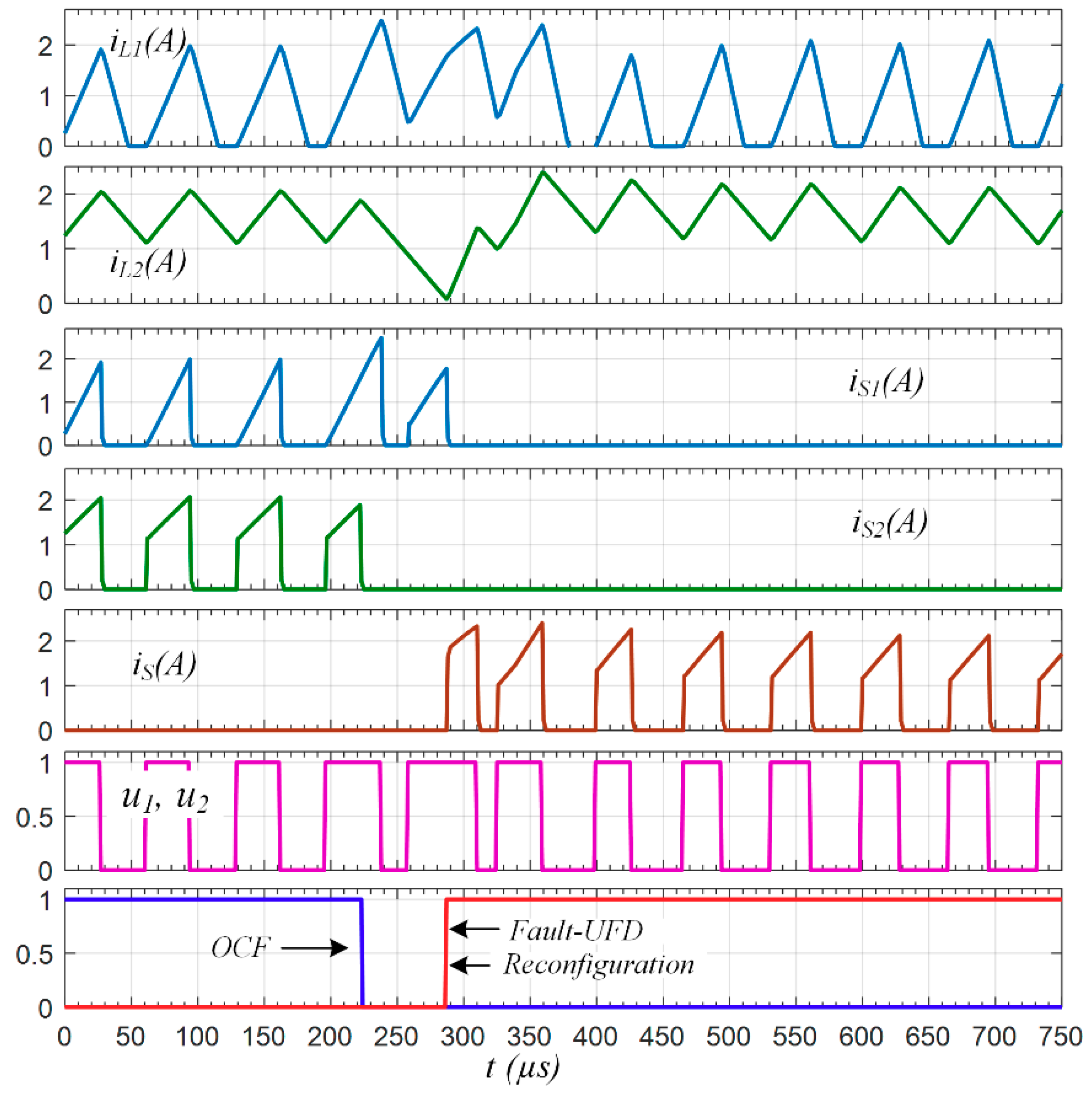
  • However, in faulty OCF conditions, in state S2 (on-check), when the converter is in the middle of Cycle 1, one of the inductor currents iL1 or iL2 decreases and the sgn signal will be equal to “0” (sgn = 0). Therefore, a transition to S4 occurs and SM stays in this state (S0→S1→S2→S4). The FAULT signal (output of the SM) goes to “1” and a fault is declared. It is noticeable that, if the fault occurs after T3, the fault will be detected by the SM (Figure 7) in the next switching period (in the next S2);
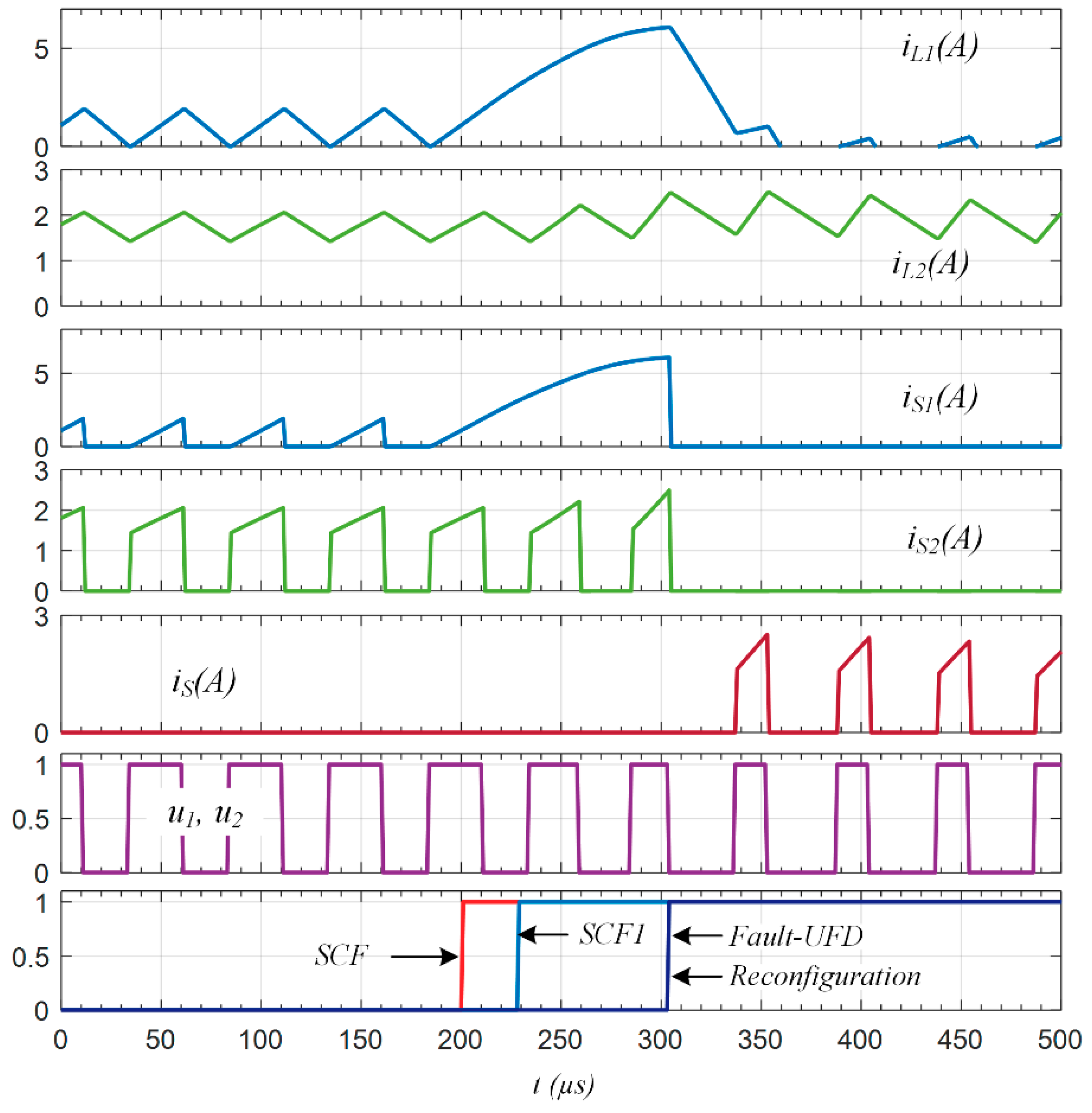
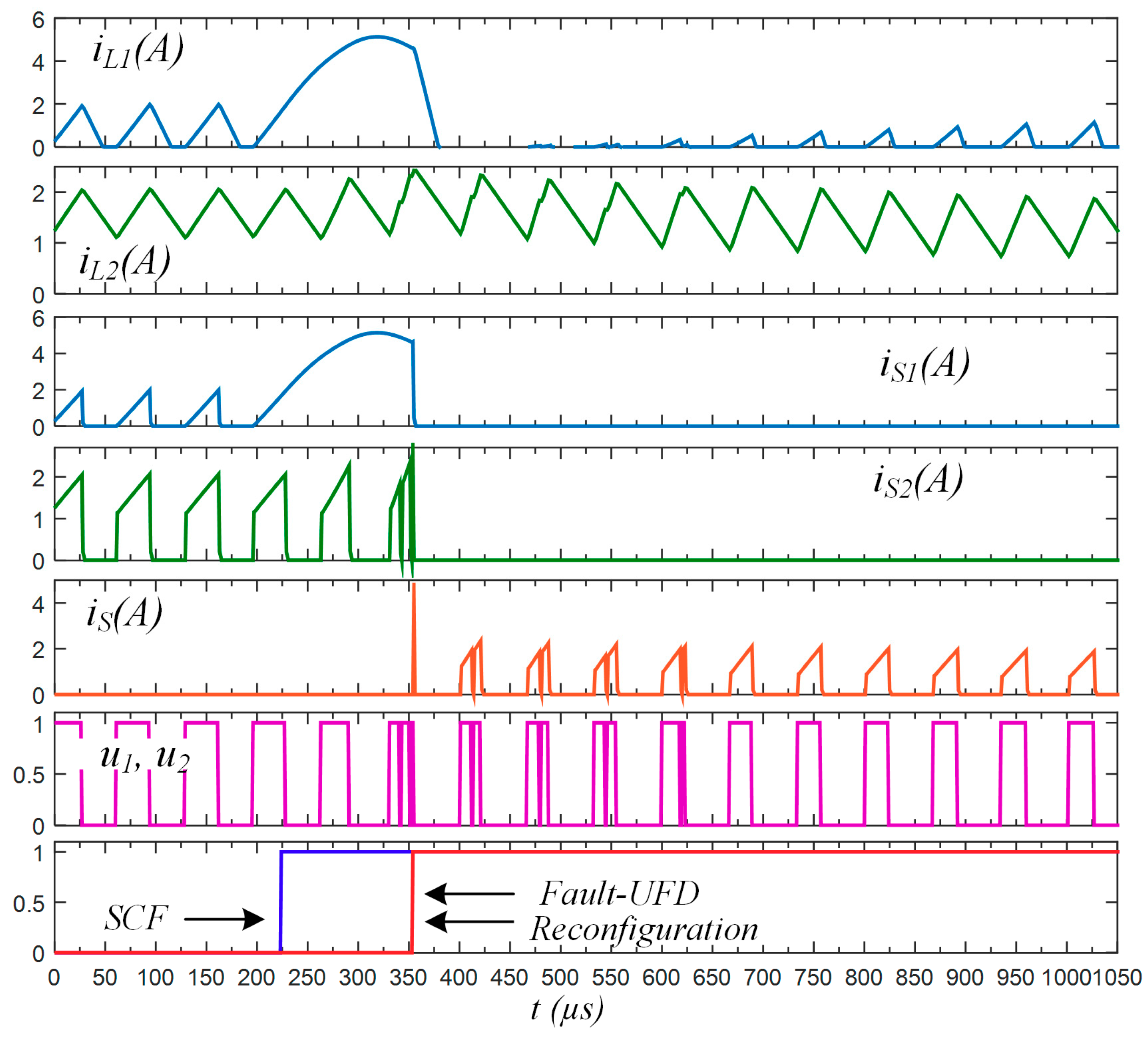
  • In the case of an SCF, after fault occurrence, the state machine continues in normal operation for some switching periods, until fuse action. When the fuse breaks, the SCF becomes an OCF. In state S2, the sgn is not equal to “1” thus a transition to S4 occurs. As for an OCF, the FAULT signal (output of the SM) goes to “1” and the fault is declared.
The proposed UFD algorithm is only able to detect a fault without fault identification and localization. However, the major advantage of the proposed UFD by comparison to the parallel FD (in Section 3.2.) is the simple implementation.
As mentioned before, the proposed UFD is applied to a fault-tolerant two-stage DC-DC converter with a redundant switch (Figure 9) to show its efficiency. In fault-tolerant operation, after fault detection, there are in general two other steps: Fault localization and system reconfiguration. For the studied converter, the post-fault reconfiguration strategy is the same, regardless of the fault localization. In post-fault operation and under synchronous control, the duty cycle d and the frequency f will be sent to the PWM block to generate the switching pattern u applied to the redundant switch SWR (see Figure 3) in order to drive the overall system [18,28]. Therefore, to guarantee service continuity of the system, we just need to detect the fault occurrence and thus, the UFD method is more suitable.
For system reconfiguration after a fault detection, there are two strategies, according to the type of fault that occurred. In the case of an OCF, the current in the faulty switch is zero and thus it can be replaced by the redundant switch immediately after fault declaration. However, in the case of an SCF, the current in the faulty switch is not zero and it increases until the fuse breaks. Therefore, the reconfiguration for post-fault operation mode cannot be done before the fuse breaks, as it takes more time compared with an OCF case. When an SCF occurs, it will become an OCF after the fuse action, so both types of faults can be detected by the proposed UFD.

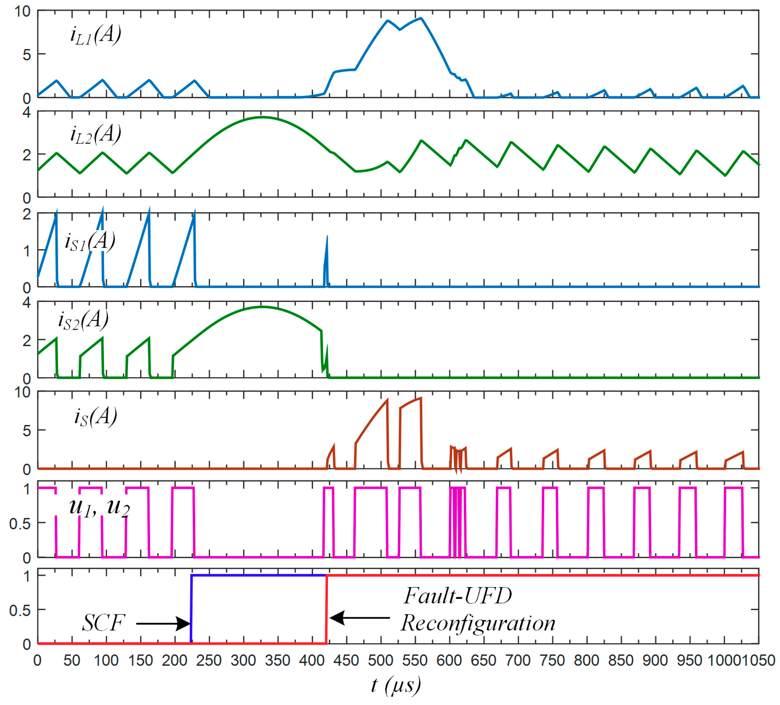
4. Simulation Results

To validate the performance of the proposed FD methods, some simulations in a Matlab Simulink (MathWorks, Natick, MA, USA) environment are performed for the fault-tolerant buck/buck–boost converter depicted in Figure 9. The elements in red are added for the fault-tolerant operation. The parameters of the converter are given in Table 1. The UFD method is applied and compared with a parallel FD approach. Details about the fault-tolerant topology (Figure 9) can be found in [25]. This topology is not detailed in this paper, dedicated to switch fault detection.
Figure 10 shows the simulation results for an OCF on SW1. The fault is detected by the two proposed methods: The parallel (OCF1) and the proposed UFD (Fault-UFD) at the same time. The fault detection signals of the two methods (OCF1 and Fault-UFD) are superposed in Figure 10. These methods declared the OCF on the SW1 very quickly, in about one switching period. The difference between the parallel and the proposed UFD fault detection is identification and localization. The proposed UFD is not capable of localizing and identifying the fault.
Figure 11 shows the simulation results for an OCF on SW2. As it can be seen in the simulation results, the OCF is detected, identified, and localized by parallel FD (OCF2 is set to “1”), while the UFD has just announced a switch fault without fault localization and fault type identification.
As these simulation results show, the proposed UFD is as fast as the parallel FD in the case of an OCF in both converters (source side and load side). The reconfiguration is applied immediately after the fault detection and the system continues to operate as the normal condition, validated by simulation results in Figure 10 and Figure 11.
Figure 12 shows the simulation results for an SCF on SW1. As it can be seen in Figure 12, the SCF is detected by the parallel FD in the next switching period after the fault occurrence. The UFD declares the fault after the fuse break, because it is not able to detect the SCF directly. When the fuse breaks and thus isolates the faulty switch, the UFD announces a switch fault (OCF), after one switching period. In the simulation, the fuse breaking time is equal to 250 µs. In the case of SCF, the reconfiguration and remedial actions must be done after the fault isolation (fuse action). Therefore, this delay of the UFD does not have an important effect on the fault-tolerant system operation.

5. Fault-Tolerant Control Implementation on an FPGA Chip

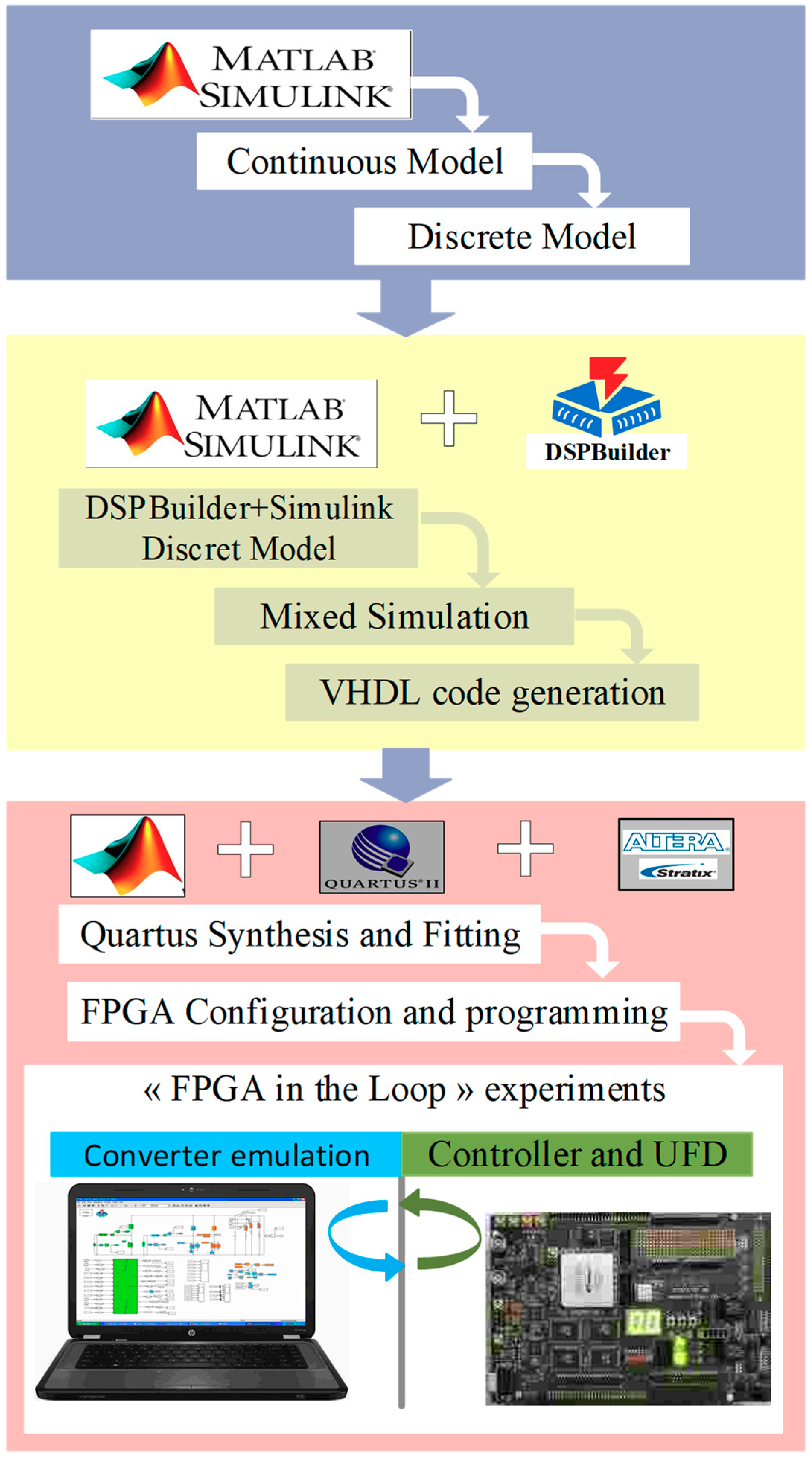
5.1. Principle of Experiment Based on Hardware-in-the-Loop (HIL)

Offline simulation of electrical and electronic applications by software such as MATLAB/Simulink and other simulation tools has greatly progressed in recent years. In some applications, such as fault detection and fault-tolerant systems, a very fast simulator is required. Although the execution time of such offline simulators is optimized, it is not always satisfactory for some critical applications. However, real-time digital HIL simulation, which has to interact with external devices, can be a reliable and cost-effective virtual scenario for rapid prototyping of electrical systems. The HIL simulation is an intermediate step before applying controllers, fault detection methods, and protective devices in a real system. Such real-time simulation can validate the new proposed algorithm under extreme conditions in a non-destructive environment. In fault-tolerant applications, to have a fast fault detection, a small simulation time step is required for the real-time simulator. Today, the FPGA (Field-Programmable Gate Array), due to their paralleled architecture, configurability, large amount of logic resources, full-custom digital-signal processing (DSP) units, and storage elements, has taken a very important role in the HIL simulation and rapid prototyping of electrical industrial applications [34,35,36,37,38].
In this paper, a design methodology based on FPGA rapid prototyping, or so-called “FPGA in the loop” [37], is used to test the proposed fault-tolerant operation. In this study, the control algorithm, the proposed UFD method, and the fault-tolerant strategies are implemented in a single FPGA chip. Figure 13 shows the different steps of the so-called “FPGA in the loop” experimentation. “FPGA in the Loop” has three steps:
  • Studied system modeling and simulation in Matlab/simulink environment, in continuous time and then in discrete time;
  • Control strategy and FD method have to be translated into a synthesizable VHDL (Very high-speed integrated circuit Hardware Description Language) model by using DSPbuilder toolbox (Intel Corporation, Santa Clara, CA, USA);
  • Development board, which contains the FPGA, can be programmed and used in the HIL simulation.
The controller, the fault diagnosis, and fault-tolerant scheme are implemented on the FPGA and the fault-tolerant converter is emulated by the PC with the Matlab/SimPowerSystems toolbox. The FPGA produces control signals and sends it to the PC as a command for the emulated converters. In our case, a Stratix III development board is used, which includes the Stratix EP3S150F1152C2 (Intel Corporation, Santa Clara, CA, USA) FPGA chip.

5.2. FPGA in the Loop Results

For HIL experimentation, the converter given in Figure 9 is considered. A classical PI (Proportional-Integral) controller is used to control the output voltage of the converter, which determines the duty cycle of the synchronous control system. In a PV system (or TEG), the operation point of the system changes with a slow dynamic compared with the UFD’s dynamic. Based on this hypothesis, for HIL tests, a fixed frequency is considered for the switching patterns. The system parameters are given in Table 1, which are the same as in the simulation tests.
Figure 14 and Figure 15 show detailed HIL results for an OCF diagnosis of SW1 and SW2 respectively. The OCFs occur at t = 223 µs. As shown in Figure 14, the inductor current iL1 and the current through the switch SW1 switched to zero after the OCF occurrence. At t = 283 µs the output signal fault goes to “1” and the fault is detected successfully after t = 63 µs, which is about one switching period (here Ts = 67 µs). After the fault diagnosis, the reconfiguration is also applied to the converter. As is illustrated in Figure 14, the switch SWR is activated at t = 283 µs when the fault signal is set up to “1”. The same scenario is repeated in Figure 15.
The HIL results for SCF diagnosis are depicted in Figure 16 and Figure 17. At t = 223 µs, the SCFs occur for SW1 (Figure 16) and SW2 (Figure 17). The inductor currents increase because of the short circuit. After 200 µs, the fuses are broken, the SCF becomes an OCF, and then the fault is declared by the UFD. Therefore, at t = 350µs, the switch SWR is activated and the converter reconfiguration is applied.
As mentioned before, in the considered fault-tolerant two-stage DC-DC converter, fault localization is not necessary. It is noticeable that in the SCF case, converter reconfiguration could not be applied before fuse action.
All these results confirm the validity of the proposed UFD.

6. Conclusions

In this paper, a unified switch fault diagnosis method for cascaded non-isolated DC-DC converters used in energy harvesting applications is proposed. The proposed UFD is compared with a parallel fault diagnosis method, which consists of two identical fault diagnosis blocks, working in parallel. The parallel method can detect, identify, and localize both types of switch faults (OCF and SCF) in less than one switching period. However, the implementation of this method is not optimized for fault-tolerant two-stage converter.
The UFD is able to detect the OCF failure without localization and identification. A short circuit fault becomes an OCF after the fuse breaks and then it can also be detected by the proposed UFD. The reconfiguration for post-fault operation for the studied two-stage DC-DC fault-tolerant cascade converter does not depend on the type and location of the fault. Therefore, the proposed UFD, with a simple implementation, is suitable for this family of converters, compared to the parallel FD method. The performances of the proposed UFD applied on a two-stage DC-DC converter are validated by the selected simulation and HIL experimentation results.

Author Contributions

All authors contributed equally to this work.

Funding

This research received no external funding.

Conflicts of Interest

The authors declare no conflict of interest.

References

  1. Qing, S.; Rezania, A.; Rosendahl, L.A.; Gou, X. An Analytical Model for Performance Optimization of Thermoelectric Generator With Temperature Dependent Materials. IEEE Access 2018, 6, 60852–60861. [Google Scholar] [CrossRef]
  2. Weng, C.C.; Huang, M.J. A simulation study of automotive waste heat recovery using a thermoelectric power generator. Int. J. Therm. Sci. 2013, 71, 302–309. [Google Scholar] [CrossRef]
  3. Korde, P.; Kamble, V. Efficient Utilization of waste Heat to Electrical Energy for Real-Time Applications. In Proceedings of the IEEE 9th International Conference on Computing, Communication and Networking Technologies (ICCCNT), Bengaluru, India, 10–12 July 2018; pp. 1–6. [Google Scholar]
  4. Das, A.; Gao, Y.; Kim, T.T.H. A 220-mv power-on-reset based self-starter with 2-nW quiescent power for thermoelectric energy harvesting systems. IEEE Trans. Circuits Syst. Regul. Pap. 2017, 64, 217–226. [Google Scholar] [CrossRef]
  5. Wang, D.; Mo, J.; Wang, X.; Ouyang, H.; Zhou, Z. Experimental and numerical investigations of the piezoelectric energy harvesting via friction-induced vibration. Energy Convers. Manag. 2018, 171, 1134–1149. [Google Scholar] [CrossRef]
  6. Katic, J.; Rodriguez, S.; Rusu, A. An efficient boost converter control for thermoelectric energy harvesting. In Proceedings of the IEEE 20th International Conference on Electronics, Circuits, and Systems (ICECS), Abu Dhabi, United Arab Emirates, 8–11 December 2013; pp. 385–388. [Google Scholar]
  7. Zurbriggen, I.G.; Ordonez, M. PV Energy Harvesting Under Extremely Fast Changing Irradiance: State-Plane Direct MPPT. IEEE Trans. Ind. Electron. 2019, 66, 1852–1861. [Google Scholar] [CrossRef]
  8. Abdelhamid, M.; Singh, R.; Qattawi, A.; Omar, M.; Haque, I. Evaluation of on-board photovoltaic modules options for electric vehicles. IEEE J. Photovolt. 2014, 4, 1576–1584. [Google Scholar] [CrossRef]
  9. Armstrong, P.; Armstrong, R.W.; Kang, R.; Camilleri, R.; Howey, D.; McCulloch, M. A reconfigurable PV array scheme integrated into an electric vehicle. In Proceedings of the IET Hybrid and Electric Vehicles Conference, London, UK, 6–7 November 2013; pp. 1–7. [Google Scholar]
  10. Kaplan, A.; Kingry, N.; Uhing, P.; Dai, R. Time-optimal path planning with power schedules for a solar-powered ground robot. IEEE Trans. Autom. Sci. Eng. 2017, 14, 1235–1244. [Google Scholar] [CrossRef]
  11. Diab-Marzouk, A.; Trescases, O. Sic-based bidirectional CUK converter with differential power processing and MPPT for a solar powered aircraft. IEEE Trans. Transport. Electrific. 2015, 1, 369–381. [Google Scholar] [CrossRef]
  12. Tran, T.V.; Chung, W.Y. High-efficient energy harvester with flexible solar panel for a wearable sensor device. IEEE Sens. J. 2016, 16, 9021–9028. [Google Scholar] [CrossRef]
  13. Brogan, Q.; O’Connor, T.; Ha, D.S. Solar and thermal energy harvesting with a wearable jacket. In Proceedings of the 2014 IEEE International Symposium on Circuits and Systems (ISCAS), Melbourne, Australia, 1–5 June 2014; pp. 1412–1415. [Google Scholar]
  14. Blaabjerg, F.; Chen, Z.; Kjaer, S.B. Power electronics as efficient interface in dispersed power generation systems. IEEE Trans. Power Electron. 2004, 19, 1184–1194. [Google Scholar] [CrossRef]
  15. Xu, C.; Pan, C.; Liu, Y.; Wang, Z.L. Hybrid cells for simultaneously harvesting multi-type energies for self-powered micro/nanosystems. Nano Energy 2012, 1, 259–272. [Google Scholar] [CrossRef]
  16. Khan, A.A.; Mahmud, A.; Ban, D.B. Evolution From Single To Hybrid Nanogenerator: A Contemporary Review On Multimode Energy Harvesting For Self-Powered Electronics. IEEE Trans. Nanotechnol. 2018, 18, 21–36. [Google Scholar] [CrossRef]
  17. Haji-Esmaeili, M.M.; Naseri, M.; Khoun-Jahan, H.; Abapour, M. Fault-Tolerant and Reliable Structure for a Cascaded Quasi-Z-Source DC-DC Converter. IEEE Trans. Power Electron. 2017, 32, 6455–6467. [Google Scholar] [CrossRef]
  18. Siouane, S.; Jovanović, S.; Poure, P. Service continuity of PV synchronous Buck/Buck-Boost converter with energy storage. Energies 2018, 11, 1369. [Google Scholar] [CrossRef]
  19. An, L.; Lu, D.D.C. Design of a single-switch DC-DC converter for a PV-battery-powered pump system with PFM+PWM control. IEEE Trans. Ind. Electron. 2015, 62, 910–921. [Google Scholar] [CrossRef]
  20. Alli, S.S.; Jovanović, S.; Poure, P.; Jamshidpour, E. MPPT and output voltage control of Photovoltaic systems using a Single-Switch DC-DC converter. In Proceedings of the 2016 IEEE International Energy Conference (ENERGCON), Leuven, Belgium, 4–8 April 2016; pp. 1–6. [Google Scholar]
  21. Jamshidpour, E.; Poure, P.; Saadate, S. Photovoltaic Systems Reliability Improvement by Real-Time FPGA-Based Switch Failure Diagnosis and Fault-Tolerant DC-DC Converter. IEEE Trans. Ind. Electron. 2015, 62, 7247–7255. [Google Scholar] [CrossRef]
  22. Jamshidpour, E.; Shahbazi, M.; Saadate, S.; Poure, P.; Gholipour, E. FPGA based fault detection and fault tolerance operation in DC-DC converters. In Proceedings of the 2014 International Symposium on Power Electronics, Electrical Drives, Automation and Motion, Ischia, Italy, 18–20 June 2014; pp. 37–42. [Google Scholar] [CrossRef]
  23. Rubino, L.; Guida, B.; Liccardo, F.; Marino, P.; Cavallo, A. Buck-boost DC-DC converter for aeronautical applications. In Proceedings of the 2010 IEEE International Symposium on Industrial Electronics (ISIE), Bari, Italy, 4–7 July 2010; pp. 2690–2695. [Google Scholar]
  24. Poon, J.; Jain, P.; Konstantakopoulos, I.C.; Spanos, C.; Panda, S.K.; Sanders, S.R. Model-Based Fault Detection and Identification for Switching Power Converters. IEEE Trans. Power Electron. 2017, 32, 1419–1430. [Google Scholar] [CrossRef]
  25. Siouane, S.; Jovanovic´, S.; Poure, P. Service continuity of PV synchronous Buck/Buck-Boost converter with energy storage. In Proceedings of the 2017 IEEE International Conference on Environment and Electrical Engineering and 2017 IEEE Industrial and Commercial Power Systems Europe (EEEIC/ICPS Europe), Milan, Italy, 6–9 June 2017; pp. 1–6. [Google Scholar]
  26. Gao, Z.; Cecati, C.; Ding, S.X. A survey of fault diagnosis and fault-tolerant techniques—Part I: Fault diagnosis with model-based and signal-based approaches. IEEE Trans. Ind. Electron. 2015, 62, 3757–3767. [Google Scholar] [CrossRef]
  27. Shahbazi, M.; Jamshidpour, E.; Poure, P.; Saadate, S.; Zolghadri, M.R. Open-and short-circuit switch fault diagnosis for nonisolated dc–dc converters using field programmable gate array. IEEE Trans. Ind. Electron. 2013, 60, 4136–4146. [Google Scholar] [CrossRef]
  28. Siouane, S.; Jovanovic´, S.; Poure, P. Open-Switch Fault-Tolerant Operation of a Two-Stage Buck/Buck–Boost Converter With Redundant Synchronous Switch for PV Systems. IEEE Trans. Ind. Electron. 2019, 66, 3938–3947. [Google Scholar] [CrossRef]
  29. Yin, H.; Zhao, C.; Li, M.; Ma, C. Utility function-based real-time control of a battery ultracapacitor hybrid energy system. IEEE Trans. Ind. Inform. 2015, 11, 220–231. [Google Scholar] [CrossRef]
  30. Ribeiro, E.; Cardoso, A.J.M.; Boccaletti, C. Open-circuit fault diagnosis in interleaved DC–DC converters. IEEE Trans. Power Electron. 2014, 29, 3091–3102. [Google Scholar] [CrossRef]
  31. Adouni, A.; Elmellah, K.; Chariag, D.; Sbita, L. DC-DC converter fault diagnostic in PV system. In Proceedings of the 2017 International Conference on Green Energy Conversion Systems (GECS), Hammamet, Tunisia, 23–25 March 2017; pp. 1–7. [Google Scholar]
  32. Givi, H.; Farjah, E.; Ghanbari, T. Switch and Diode Fault Diagnosis in Nonisolated DC-DC Converters Using Diode Voltage Signature. IEEE Trans. Ind. Electron. 2018, 65, 1606–1615. [Google Scholar] [CrossRef]
  33. Jamshidpour, E.; Poure, P.; Saadate, S. Unified Switch Fault Detection for Cascaded Non-Isolated DC-DC Converters. In Proceedings of the 2018 IEEE International Conference on Environment and Electrical Engineering and 2018 IEEE Industrial and Commercial Power Systems Europe (EEEIC/ICPS Europe), Palermo, Italy, 12–15 June 2018; pp. 1–6. [Google Scholar]
  34. Roshandel Tavana, N.; Dinavahi, V. A General Framework for FPGA-Based Real-Time Emulation of Electrical Machines for HIL Applications. IEEE Trans. Ind. Electron. 2015, 62, 2041–2053. [Google Scholar] [CrossRef]
  35. Buccella, C.; Cecati, C.; Latafat, H. Digital Control of Power Converters-A Survey. IEEE Trans. Ind. Informat. 2012, 8, 437–447. [Google Scholar] [CrossRef]
  36. Monmasson, E.; Idkhajine, L.; Cirstea, M.; Bahri, I.; Tisan, A.; Naouar, M.W. FPGAs in Industrial Control Applications. IEEE Trans. Ind. Informat. 2011, 7, 224–243. [Google Scholar] [CrossRef]
  37. Karimi, S.; Poure, P.; Saadate, S. An HIL-Based Reconfigurable Platform for Design, Implementation, and Verification of Electrical System Digital Controllers. IEEE Trans. Ind. Electron. 2010, 57, 1226–1236. [Google Scholar] [CrossRef]
  38. Potamianos, P.; Mitronikas, E.; Safacas, A. Open-Circuit Fault Diagnosis for Matrix Converter Drives and Remedial Operation Using Carrier-Based Modulation Methods. IEEE Trans. Ind. Electron. 2014, 61, 531–545. [Google Scholar] [CrossRef]
Figure 1. Two-stage non-isolated DC-DC converters used in energy harvesting systems.
Electronics 08 00293 g001
Figure 2. Non-isolated single-switch DC-DC converters and common shape inductance current [22].
Electronics 08 00293 g002
Figure 3. Fault-tolerant cascaded non-isolated DC-DC circuit for energy harvesting systems, proposed in [25].
Electronics 08 00293 g003
Figure 4. Parallel fault detection method block diagram.
Electronics 08 00293 g004
Figure 5. Boost converter and operation cycles.
Electronics 08 00293 g005
Figure 6. Two-stage non-isolated DC-DC converter under synchronous control.
Electronics 08 00293 g006
Figure 7. State machine used for the proposed Unified Switch Fault Diagnosis (UFD).
Electronics 08 00293 g007
Figure 8. Switching pattern, inductor currents and input signals for the state machine. (a) Open-circuit fault (OCF) on SW1. (b) OCF on SW2.
Electronics 08 00293 g008
Figure 9. Studied fault-tolerant cascaded DC-DC converter.
Electronics 08 00293 g009
Figure 10. Simulation results, OCF diagnosis of SW1.
Electronics 08 00293 g010
Figure 11. Simulation results; OCF diagnosis of SW2.
Electronics 08 00293 g011
Figure 12. Simulation result; short-circuit fault (SCF) diagnosis of SW1.
Electronics 08 00293 g012
Figure 13. “FPGA in the Loop” prototyping test.
Electronics 08 00293 g013
Figure 14. “FPGA in the Loop” results; OCF diagnosis on SW1.
Electronics 08 00293 g014
Figure 15. “FPGA in the Loop” results; OCF diagnosis of SW2.
Electronics 08 00293 g015
Figure 16. “FPGA in the Loop” results; SCF diagnosis of SW1.
Electronics 08 00293 g016
Figure 17. “FPGA in the Loop” results; OCF diagnosis of SW2.
Electronics 08 00293 g017
Table 1. Simulation parameters for the fault-tolerant cascaded DC-DC converter.
ElementsVinRLL2C2VBL1C1fs
Value8 V25 Ω100 µH22 µF12 V50 µH100 µF20 KHz

