Article

Sufficient Condition-Based Stability Analysis of a Power Converter Applied Switching Transient Waveform Modification Using Kharitonov’s Theorem

School of Automation Science and Electrical Engineering, Beihang University, Beijing 100191, China
*
Author to whom correspondence should be addressed.
Electronics 2019, 8(2), 245; https://doi.org/10.3390/electronics8020245
Submission received: 31 December 2018 / Revised: 15 February 2019 / Accepted: 19 February 2019 / Published: 21 February 2019
(This article belongs to the Special Issue Advanced Power Conversion Technologies)

Abstract

:
The rapid switching action of power metal-oxide-semiconductor field-effect transistor (MOSFET) causes high-level electromagnetic interference (EMI) in power converters. The switching transient waveform modification method realized by closed-loop gate drive has been recognized as an effective high-frequency EMI reduction approach. However, feedback control of power MOSFET in the saturation region would introduce stability problems. This paper presents a sufficient condition-based stability analysis of all the operating points during turn-off using Kharitonov’s theorem. Firstly, a small-signal MOSFET model during turn-off was used to derive the closed-loop system transfer function. The nonlinear capacitances and the rest constant parameters of the small-signal model were determined based on the device characteristics and the expected outcome of the drain-source voltage. Then we split the turn-off switching transient into several subintervals, during which the system characteristic equation became an interval polynomial due to the nonlinear capacitances. Finally, Kharitonov’s theorem was applied in each subinterval to evaluate the stability, thereby achieving the overall system stability analysis during turn-off. Experiments were conducted to investigate the system’s stability and the results confirmed the validity of the proposed analysis. This work presents an implementable design guideline for the applied switching transient waveform modification of power converters via closed-loop gate drive.

1. Introduction

The high switching speeds of power metal-oxide-semiconductor field-effect transistor (MOSFET) result in serious interference in power converters. Generally, interference suppression can be achieved by applying electromagnetic interference (EMI) filters at a cost of additional space for installation [1,2,3]. The closed-loop gate drive method has been successfully applied to regulate the switching trajectory of insulated-gate bipolar transistor (IGBT)/MOSFETs in power converters [4,5,6,7]. Feedback control of switching devices in the saturation region is employed to modify the switching transient waveform according to a Gaussian S-shaped reference for electromagnetic interference suppression [7,8]. The effect of reduced EMI generation is remarkable. However, the stability issues introduced by the feedback control should be seriously considered in circuit design.
In [9], the stability of the drive system was investigated using standard control theory methods. The enlightening contribution of the work was the application of the IGBT small-signal model for the system open- and closed-loop transfer functions. The parameters of the feedback circuit and IGBT variation on the stability of the drive system were researched by root locus plots. However, the nonlinear drain-source and drain-gate capacitances of the small-signal model depended on the switching conditions, especially the drain-source voltage. It is impracticable to investigate the effect of one parameter’s variation on stability while keeping other parameters fixed. To guarantee the stability of the controller in the worst case conditions, three major operating points during turn-off were chosen to represent the whole switching process [10]. The values of the nonlinear parameters around the operating points were determined and hence a stability analysis of different operating points was achieved using the Bode plots. However, the exact operating points were difficult to choose. Furthermore, the corresponding small signal model parameters rely on the accuracy of the device model and would not be easily extracted. The work in [11] followed from [10] and made some improvements. To overcome the aforementioned limitations, different estimation ranges were attached to the corresponding parameters for each operating point. In this way the system closed-loop transfer function with coefficients varying within known intervals was obtained. Then a robust stability analysis of each operating point was performed by using Kharitonov’s theorem, which guarantees the stability of an interval polynomial. However, limitations also exist with this approach. The selection of operating points and determination of value ranges for corresponding parameters is mainly based on practical IGBT behaviors, the shape of the reference waveform, and the designer’s experience. Hence, the approach is difficult to implement in practice and the analysis results may not be able to judge the system stability during the whole turn-off process. In [12], the measured nonlinear device parameters were modelled via curve-fit. Operating point variation on the poles and zeros was investigated to achieve the stability analysis during turn-off.
It has been proved that a pulse width modulation (PWM) signal with Gaussian S-shaped switching transients can promise remarkably high-frequency EMI suppression [7,13]. This signal was used as the reference waveform for the closed-loop gate drive circuit in the following investigation. This paper follows from [11] by using Kharitonov’s Theorem to achieve a sufficient condition-based stability analysis of the applied switching transient waveform modification of a power converter. In Section 2, a closed-loop gate drive prototype for switching transient waveform modification is presented. The system closed-loop transfer function was derived by applying a conventional MOSFET small-signal model. In Section 3, a parameter determination procedure based on the device characteristics and the expected outcome of the drain-source voltage is presented. In Section 4, a stability analysis of a standard chopper under different controller designs using the proposed method is presented. The results of the theoretical analysis were confirmed by experiments presented in the last section.

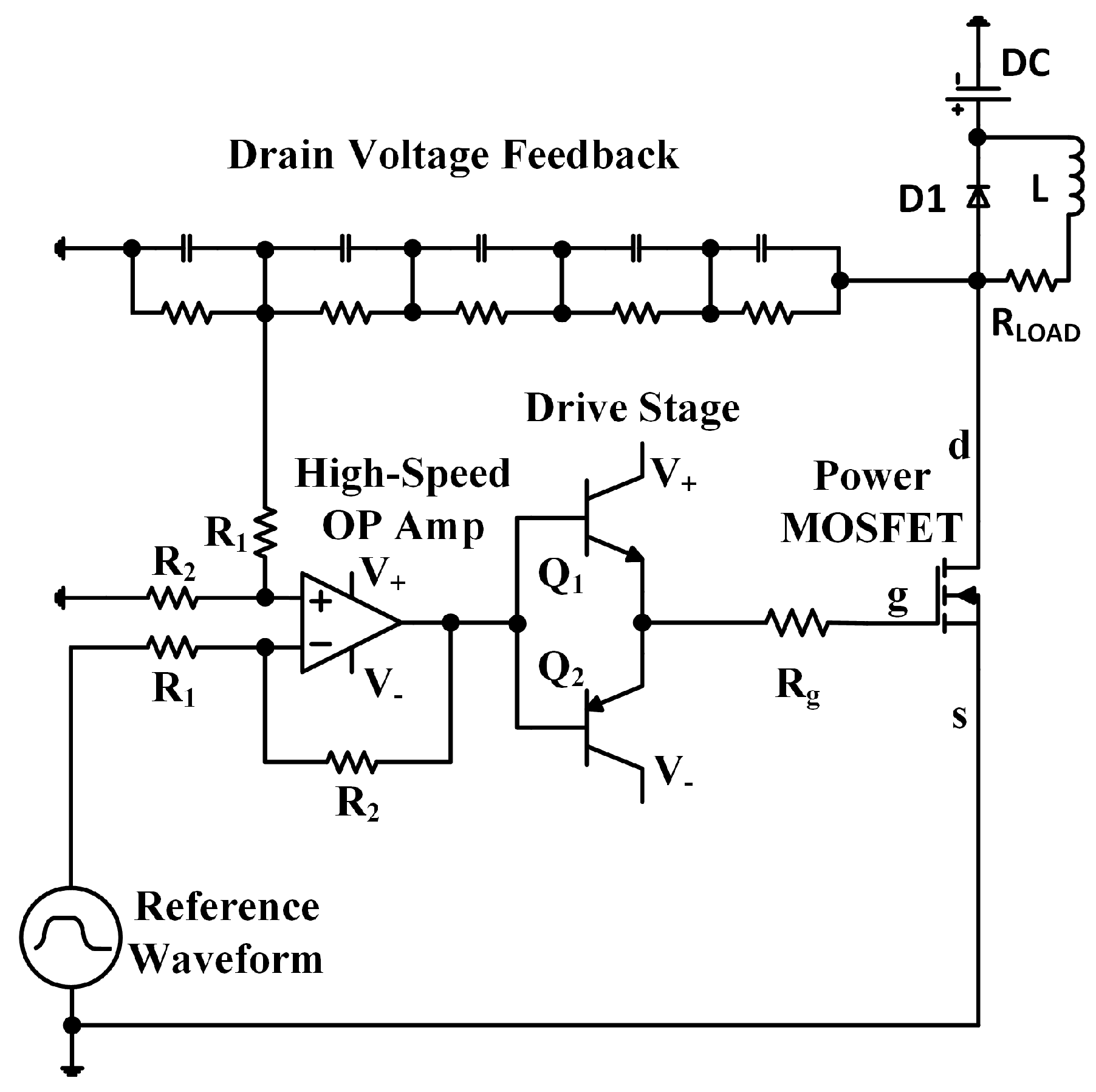
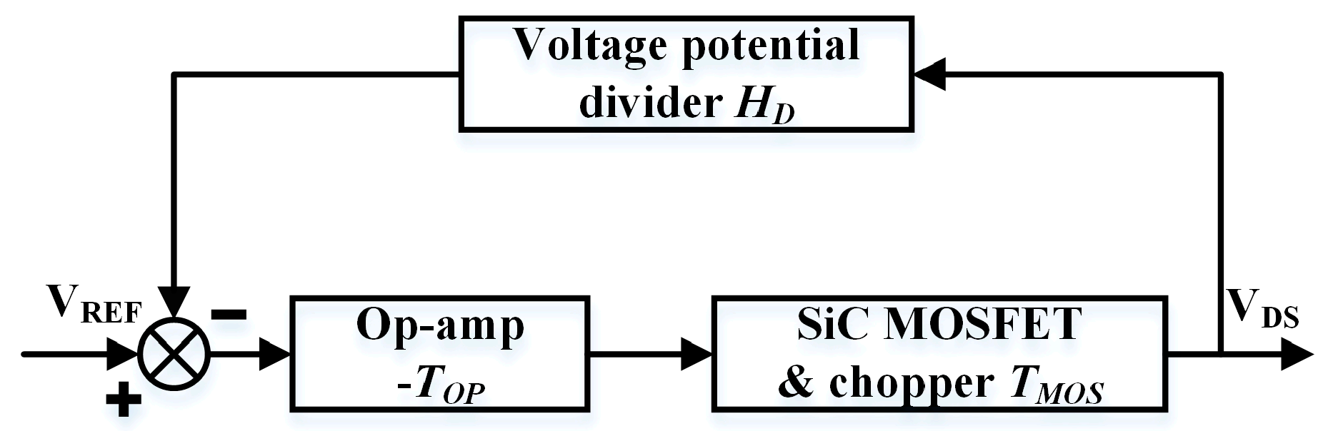
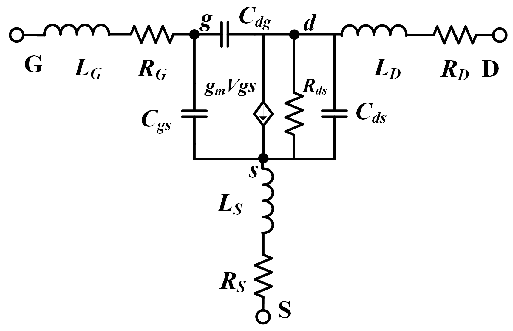
2. Modeling of Closed-Loop Gate Drive

Most power converters can be reduced to the standard chopper cell to investigate the transient response of power MOSFETs/IGBTs. Therefore, a standard chopper cell was chosen for the illustration of the drive circuit modeling. Figure 1 shows the chopper in detail, including a freewheeling diode, an inductive load, a power MOSFET, and the closed-loop gate drive. The drive circuit followed the same structural outline with that proposed in [5]. A feedback control was used to modify the drain-source voltage according to the reference waveform. The drain voltage feedback formed with resistors and capacitors was applied to provide a scaled drain voltage. An op-amp with a high bandwidth and a wide voltage swing was applied to obtain the error signal by comparing the scaled drain voltage with the reference waveform. The drive stage was an emitter follower formed with two transistors and provided the necessary current gain for MOSFET driving. The gate resistor Rg played an important role in stability control.
The drive circuit was partitioned into the blocks displayed in Figure 2. The drive stage had a negligible effect on the input voltage and was ignored when modeling. The drain voltage feedback term composed of resistors and capacitors was modelled as a low-pass filter with a cut-off frequency of fFB and a gain of α. The transfer function HD is given by:
H D = α / ( 1 + s / ( 2 π f F B ) )
Likewise, the summing op-amp is modelled as a low-pass filter, taking into account the bandwidth fOP and the gain AOP. The transfer function TOP is given by:
T O P = A O P / ( 1 + s / ( 2 π f O P ) )
A small-signal MOSFET model, as shown in Figure 3, takes into account the internal gate resistance RG, source resistance RS, drain resistance RD, output resistance Rds, the terminal stray inductances LG, LS, LD, the drain-source Cds, drain-gate Cdg, and gate-source Cgs capacitances, as well as the transconductance gm. In the following analysis, RG should consist of both the external and internal gate resistances. Additionally, the terminal stray inductances should include the drive circuit stray inductances. The small-signal conditions are different for the turn-on and turn-off process [10]. In this study, we illustrated the stability investigation based on the turn-off process. The same analysis procedure can be performed for the turn-on process.
The chopper under closed-loop gate drive (Figure 2), had an inductive load that can be regarded as a current source at turn-off. Therefore, the connection between the drain terminal and the inductive load was an open-circuit in small signal analysis. At turn-off, the node voltage equations are given by:
( m 1 + s C g s + s C d g ) V g s C d g V D S s C g s V s = m 1 V G S
( g m s C d g ) V g + ( s C d g + m 2 ) V D S ( g m + m 2 ) V s = 0
( g m + s C g s ) V g m 2 V D S + ( m 3 + m 2 + s C d s + g m ) V s = 0
where m1 represents 1/(RG + s × LG), m2 represents (1/Rds + s × Cds), and m3 represents 1/(RS + s × LS). Then the transfer function from VGS to VDS can be derived from (3), (4), and (5), as given by:
T M O S = V D S V G S = a 3 s 3 + a 2 s 2 + a 1 s + a 0 b 3 s 3 + b 2 s 2 + b 1 s + b 0
with the coefficients:
a 0 = R d s g m a 1 = R S ( C d g + C g s ) + R d s C d g ( 1 + R S g m ) a 2 = L S C P + R S R d s C T a 3 = L S R d s C T b 0 = 1 b 1 = ( R G + R S ) C P + R d s ( C d g + C d s ) b 2 = ( L G + L S ) C P + R d s ( R G + R S ) C T b 3 = R d s ( L G + L S ) C T C P = C d g + C g s + C d g R d s g m C T = C d g C d s + C d g C g s + C d s C g s
With all the blocks are modelled in the small-signal domain, we get the system closed-loop transfer function, as given by:
T C L = V D S V R E F = T O P T M O S 1 H D T O P T M O S = d 4 s 4 + d 3 s 3 + d 2 s 2 + d 1 s + d 0 c 5 s 5 + c 4 s 4 + c 3 s 3 + c 2 s 2 + c 1 s + c 0
with the coefficients:
d 0 = 4 π 2 a 0 A O P f O P f F B d 1 = 2 π A O P f O P ( a 0 + 2 π a 1 f F B ) d 2 = 2 π A O P f O P ( a 1 + 2 π a 2 f F B ) d 3 = 2 π A O P f O P ( a 2 + 2 π a 3 f F B ) d 4 = 2 π a 3 A O P f O P c 0 = 4 π 2 f O P f F B ( α a 0 A O P b 0 ) c 1 = 4 π 2 f O P f F B ( α a 1 A O P b 1 ) 2 π b 0 f T c 2 = b 0 + 4 π 2 f O P f F B ( α a 2 A O P b 2 ) 2 π b 1 f T c 3 = b 1 + 4 π 2 f O P f F B ( α a 3 A O P b 3 ) 2 π b 2 f T c 4 = b 2 2 π b 3 f T c 5 = b 3 f T = f O P + f F B
where VREF represents the reference voltage.

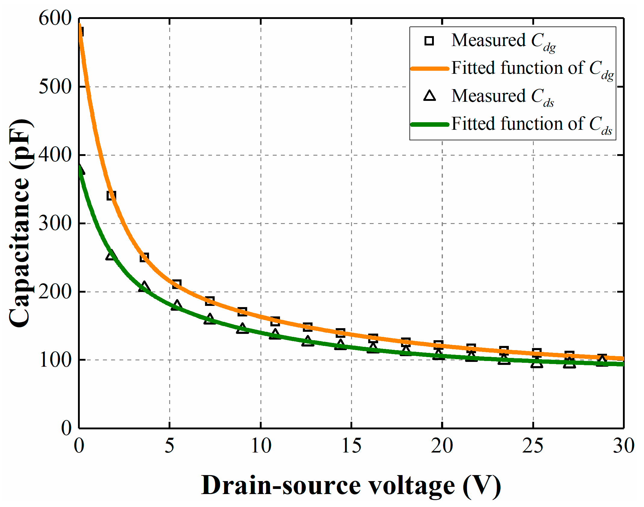
3. Determination of the Parameters

Most of the small-signal model parameters can be directly extracted from the device datasheet and the device SPICE model. However, the nonlinear drain-source Cds and drain-gate Cdg capacitances that depend on the drain-source voltage need to be seriously treated. It is noteworthy that the drain-source voltage has an expected trajectory under closed-loop gate drive, which provides an advantage when evaluating the voltage-dependent capacitances. The determination procedure of small signal parameters is illustrated with the following conditions. The power MOSFET used in this paper was an IRL2703 module. The DC voltage source was set to 30 V. The reference waveform was a PWM signal with Gaussian S-shaped switching transients that can be expressed by convolution between a Gaussian function and a rectangular signal g(t), as given by:
s w ( t ) = ( e τ 2 / 2 σ t 2 / ( σ t 2 π ) ) g ( t )
where τ represents the switching time and σt = τ/4. The Gaussian function is infinitely differentiable and hence the reference waveform could provide a remarkable EMI suppression [7,13]. The switching frequency, switching time, and duty cycle of the reference waveform are 400 kHz, 450 ns, and 0.5, respectively.
According to the device SPICE model and datasheet, RG, RD, RS, LG, LD, and LS can be directly estimated to be 4.72 Ω, 0.0001 Ω, 0.03 Ω, 15 nH, 4.5 nH, and 7.5 nH, respectively. A parametric curve tracer was used to obtain the output characteristics and the transfer characteristics. The curves of the input capacitance Ciss, output capacitance Coss, and reverse transfer capacitance Crss versus VDS were also measured using the curve tracer. Note that Rds and gm can be approximated by dVDS/dID and dID/dVGS, respectively. Therefore, Rds can be estimated from the output characteristics and can be regarded as a constant with a value of 10 kΩ. The transfer characteristics of the MOSFET can be used to estimate gm to be 13 S in the saturation region. Cgs, Cds, and Cdg can be estimated by the capacitance curves (Cgs = CissCrss, Cdg = Crss, and Cds = Coss - Crss). Therefore, Cgs can be regarded as a constant during turn-off with a value of 350 pF. The nonlinear capacitances Cds and Cdg mainly depend on the drain-source voltage and can be approximated via curve-fit, as given by:
C d s = 144.79 e V D S / 1.53 + 149.69 e V D S / 9.52 + 87.48
C d g = 331.65 e V D S / 1.61 + 1 171.25 e V D S / 12.11 + 87.69
where the drain-source voltage VDS increases from 0 to 30 V according to (10). The measured nonlinear capacitances and the fitted functions are shown in Figure 4.

4. Stability Analysis

4.1. Kharitonov’s Theorem

Consider an interval polynomial,
h ( s ) = j = 0 n a j s j
where the value range of aj is [εj, βj]. There exists the following necessary and sufficient condition for stability.
Kharitonov’s Theorem [14]: The polynomial family defined by (13) is Hurwitz stable if and only if four polynomials, shown as,
h 1 ( s ) = β 0 + ε 1 s + ε 2 s 2 + β 3 s 3 + β 4 s 4 + ε 5 s 5 +
h 2 ( s ) = β 0 + β 1 s + ε 2 s 2 + ε 3 s 3 + β 4 s 4 + β 5 s 5 +
h 3 ( s ) = ε 0 + β 1 s + β 2 s 2 + ε 3 s 3 + ε 4 s 4 + β 5 s 5 +
h 4 ( s ) = ε 0 + ε 1 s + β 2 s 2 + β 3 s 3 + ε 4 s 4 + ε 5 s 5 +
are Hurwitz stable.

4.2. Sufficient Condition-Based Stability Analysis

Four designs of closed-loop gate drive for power MOSFET are provided in Table 1. The DC voltage and reference waveform remain the same as in Section 3. The turn-off switching transient can be divided into five subintervals. The minimum and maximum values of VDS, Cdg, and Cds in each subinterval can be calculated by (10), (11), and (12), as shown in Table 2. For different circuit designs, the ranges of the parameters c0, c1, c2, c3, c4, and c5 in (8) can be obtained by substituting the parameters in Table 1 and Table 2 into (7) and (9). Therefore, the denominator of the system closed-loop transfer function can be regarded as an interval polynomial in each subinterval. Kharitonov’s theorem can be performed to assess the stability of the system during every subinterval, thereby achieving the overall system stability analysis during turn-off switching transient. From Kharitonov’s theorem, the stability of the system during each subinterval can be checked by testing the stability of the following four polynomials:
c 0 , max + c 1 , min s + c 2 , min s 2 + c 3 , max s 3 + c 4 , max s 4 + c 5 , min s 5
c 0 , max + c 1 , max s + c 2 , min s 2 + c 3 , min s 3 + c 4 , max s 4 + c 5 , max s 5
c 0 , min + c 1 , max s + c 2 , max s 2 + c 3 , min s 3 + c 4 , min s 4 + c 5 , max s 5
c 0 , min + c 1 , min s + c 2 , max s 2 + c 3 , max s 3 + c 4 , min s 4 + c 5 , min s 5
where cj,max and cj,min represent the maximum and minimum of cj, respectively. In order to highlight the analysis process, the ranges of the parameters c0, c1, c2, c3, c4, and c5 during (0, 100 ns) under Design I are provided in Table 3. It was found that Design I was stable during the first subinterval according to (18), (19), (20), and (21).
The theoretical analysis showed that Design I, Design II, Design III, and Design IV were stable during the turn-off switching transients. It should be noted that the proposed stability analysis approach is a sufficient condition. The fewer the number of subintervals, the stronger the sufficient condition.

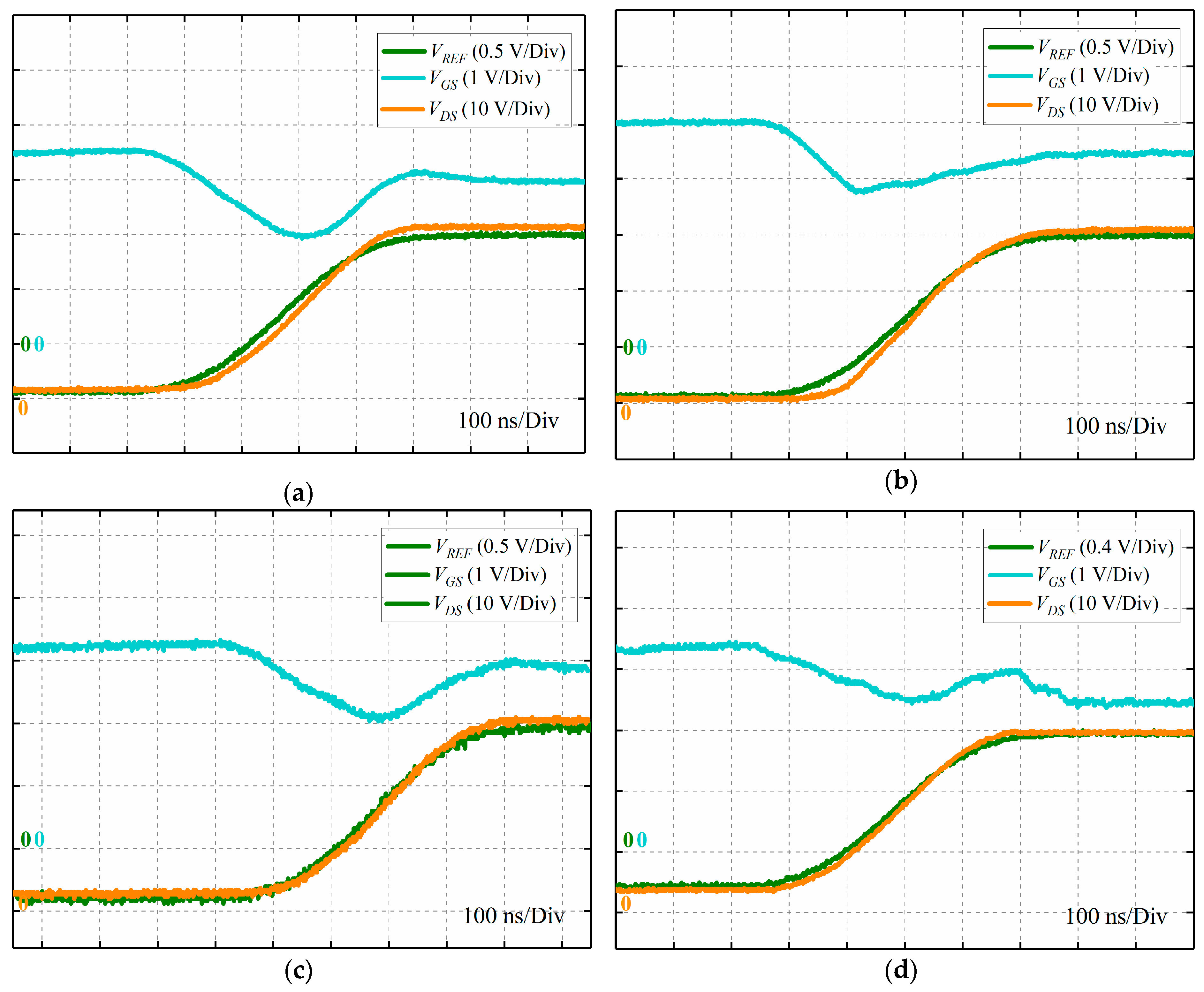
5. Experimental Results

A chopper with an inductive load was tested. The MOSFET was an IRL2703. The drain voltage feedback term was realized by resistors and capacitances. A THS3091 operational amplifier was chosen to provide the necessary gains and bandwidths. The DC voltage was set to be 30 V. The reference waveform was formed with an arbitrary waveform generator. It has been proposed in [11] that the stability of the closed-loop gate drive for switching transient modification can be accessed by the appearance of the gate-source voltage with the reference voltage as input. The switching waveforms during turn-off under Design I, Design II, Design III, and Design IV are shown in Figure 5. For Design I, it can be seen that the drain-source voltage had a Gaussian S-shaped switching transient with smooth corners. There was no oscillation in the gate-source voltage waveform. For Design II, though some tracking errors exist at the bottom corner of the drain-source voltage, the gate-source voltage was stably damped. Compared with Design I, Design III was stable with a smaller gate resistance, resulting in smaller tracing errors, as shown in Figure 5c. Compared with Design II, Design IV had a smaller gain in drain voltage feedback. No oscillation was identified in Figure 5d and hence Design IV was stable. All the experimental results confirmed the theoretical analysis.

6. Conclusions

The closed-loop gate drive was applied for the switching transient waveform modification of power converters. This paper presents an implementable approach to assess the system’s stability during the switching transient. Although the approach was a sufficient condition, it still holds great significance for drive circuit design. A stable system guarantees well-damped switching transient waveforms, whereas possible tracking errors may exist and result in a negative impact on the performance of EMI mitigation. Future works will explore the behavior of the drive circuit during switching transients.

Author Contributions

Conceptualization, T.C. and Q.M.; methodology, T.C.; validation, T.C., Q.M. and P.X.; investigation, T.C.; writing—original draft preparation, T.C.; writing—review and editing, T.C., Q.M. and P.X.

Funding

This research received no external funding.

Acknowledgments

The authors would like to thank Beihang University, Beijing, China for the financial support in executing this work successfully. This work has been carried out as a part of research work in the School of Automation Science and Electrical Engineering, Beihang University, Beijing, China.

Conflicts of Interest

The authors declare no conflict of interest.

References

  1. Zhu, H.; Liu, D.; Zhang, X.; Qu, F. Reliability of Boost PFC Converters with Improved EMI Filters. Electronics 2018, 7, 413. [Google Scholar] [CrossRef]
  2. Varajão, D.; Esteves Araújo, R.; Miranda, L.M.; Peças Lopes, J.A. EMI Filter Design for a Single-stage Bidirectional and Isolated AC–DC Matrix Converter. Electronics 2018, 7, 318. [Google Scholar] [CrossRef]
  3. Giglia, G.; Ala, G.; Di Piazza, M.C.; Giaconia, G.C.; Luna, M.; Vitale, G.; Zanchetta, P. Automatic EMI Filter Design for Power Electronic Converters Oriented to High Power Density. Electronics 2018, 7, 9. [Google Scholar] [CrossRef]
  4. John, V.; Suh, B.; Lipo, T.A. High-performance Active Gate Drive for high-power IGBT’s. IEEE Trans. Ind. Appl. 1999, 35, 1108–1117. [Google Scholar] [CrossRef]
  5. Palmer, P.R.; Rajamani, H.S. Active Voltage Control of IGBTs for High Power Applications. IEEE Trans. Power Electron. 2004, 19, 894–901. [Google Scholar] [CrossRef]
  6. Chen, L.; Peng, F.Z. Closed-loop Gate Drive for High Power IGBTs. In Proceedings of the 24th Annual IEEE Applied Power Electronics Conference and Exposition, Washington, DC, USA, 15–19 February 2009; pp. 1331–1337. [Google Scholar]
  7. Patin, N.; Vinals, M.L. Toward an Optimal Heisenberg’s Closed-loop Gate Drive for Power MOSFETs. In Proceedings of the 38th Annual Conference on IEEE Industrial Electronics Society, Montreal, QC, Canada, 25–28 October 2012; pp. 828–833. [Google Scholar]
  8. Yang, X.; Yuan, Y.; Zhang, X.; Palmer, P.R. Shaping High-power IGBT Switching Transitions by Active Voltage Control for Reduced EMI Generation. IEEE Trans. Ind. Appl. 2015, 51, 1669–1677. [Google Scholar] [CrossRef]
  9. Palmer, P.R.; Wang, Y.; Abu-khaizaran, M. Design of the Active Voltage Controller for Series IGBTs. In Proceedings of the 35th Annual Power Electronics Specialists Conference, Aachen, Germany, 20–25 June 2004; pp. 3248–3254. [Google Scholar]
  10. Wang, Y.; Palmer, P.R.; Bryant, A.T.; Finney, S.J.; Abu-Khaizaran, M.S.; Li, G. An Analysis of High-power IGBT Switching Under Cascade Active Voltage Control. IEEE Trans. Ind. Appl. 2009, 45, 861–870. [Google Scholar] [CrossRef]
  11. Yang, X.; Yuan, Y.; Long, Z.; Goncalves, J.; Palmer, P.R. Robust Stability Analysis of Active Voltage Control for High-power IGBT Switching by Kharitonov’s Theorem. IEEE Trans. Power Electron. 2016, 31, 2584–2595. [Google Scholar] [CrossRef]
  12. Groeger, J.; Wicht, B.; Norling, K. Dynamic Stability of a Closed-loop Gate Driver Enabling Digitally Controlled Slope Shaping. In Proceedings of the 13th Conference on Ph.D. Research in Microelectronics and Electronics, Giardini Naxos, Italy, 12–15 June 2017; pp. 61–64. [Google Scholar]
  13. Costa, F.; Magnon, D. Graphical Analysis of the Spectra of EMI Sources in Power Electronics. IEEE Trans. Power Electron. 2005, 20, 1491–1498. [Google Scholar] [CrossRef]
  14. Kharitonov, V.L. Asymptotic Stability of an Equilibrium Position of a Family of Systems of Differential Equations. Differ. Uravn. 1978, 14, 1483–1485. [Google Scholar]
Figure 1. A standard chopper cell applied closed-loop gate drive for switching transient modification.
Electronics 08 00245 g001
Figure 2. Control system representation of a MOSFET under closed-loop gate drive.
Electronics 08 00245 g002
Figure 3. Conventional small-signal model of power MOSFETs.
Electronics 08 00245 g003
Figure 4. Comparison between measurement and modeling of the nonlinear capacitances of the power MOSFET.
Electronics 08 00245 g004
Figure 5. Turn-off switching transient waveforms of power MOSFET: (a) VDS, VREF, and VGS waveforms under Design I; (b) VDS, VREF, and VGS waveforms under Design II; (c) VDS, VREF, and VGS waveforms under Design III; (d) VDS, VREF, and VGS waveforms under Design IV.
Electronics 08 00245 g005
Table 1. Designs of the closed-loop gate drive circuit.
Circuit DesignsDrain Voltage FeedbackOp-AmpGate Resistance
DeviceRCTHS3091R
αfFB (MHz)AOPfOP (MHz)Rg (Ω)
Design I1/2020820010
Design II1/20201016010
Design III1/202082005
Design IV1/25201016010
Table 2. Range of the nonlinear capacitances in each subinterval.
Subinterval0–100 ns100–200 ns200–300 ns300–400 ns400–500 ns
MinMaxMinMaxMinMaxMinMaxMinMax
VDS (V)02.182.189.599.5920.2920.2927.7627.7630
Cdg (pF)316.36590.59166.12316.36119.75166.12104.99119.75102.07104.99
Cds (pF)241.37381.97142.39241.37105.23142.3995.57105.2393.8895.57
Table 3. Ranges of c0, c1, c2, c3, c4, and c5 during (0, 100 ns) under Design I.
Subinterval0–100 ns
MinMax
c0−8.2 × 10²¹−8.2 × 10²¹
c1−1.8 × 10¹⁴−9.6 × 10¹³
c2−1.8 × 10¹⁶−9.8 × 10⁵
c3−0.0037−0.002
c4−2 × 10⁻¹²−1.1 × 10⁻¹²
c5−1.3 × 10⁻²²−6.1 × 10⁻²³

