Article

Voltage Multiplier Cell-Based Quasi-Switched Boost Inverter with Low Input Current Ripple

1
Faculty of Electrical and Electronics Engineering, Ho Chi Minh City University of Technology and Education, 1 Vo Van Ngan Stress, Thu Duc District, Ho Chi Minh City 700000, Vietnam
2
Department. of Electrical Engineering, Chosun University, 309 Pilmun-daero, Dong-gu, Gwangju 61542, Korea
*
Author to whom correspondence should be addressed.
Electronics 2019, 8(2), 227; https://doi.org/10.3390/electronics8020227
Submission received: 21 January 2019 / Revised: 14 February 2019 / Accepted: 15 February 2019 / Published: 18 February 2019
(This article belongs to the Special Issue Power Converters in Power Electronics)

Abstract

:
A novel single-phase single-stage voltage multiplier cell-based quasi-switched boost inverter (VMC-qSBI) is proposed in this paper. By adding the voltage multiplier cell to the qSBI, the proposed VMC-qSBI has the following merits; a decreased voltage stress on an additional switch, a high voltage gain, a continuous input current, shoot through immunity, and a high modulation index. A new pulse-width modulation (PWM) control strategy is presented for the proposed inverter to reduce the input current ripple. To improve the voltage gain of the proposed inverter, an extension is addressed by adding the VMCs. The operating principle, steady-state analysis, and impedance parameter design guideline of the proposed inverter are presented. A comparison between the proposed inverter and other impedance source-based high-voltage gain inverters is shown. Simulation and experimental results are provided to confirm the theoretical analysis.

1. Introduction

In recent years, many dc–ac power conversion topologies have attracted the interest of researchers for various applications, such as ac motor drives, uninterruptible power supplies, hybrid electric vehicles, and renewable energy systems [1]. Voltage source inverters (VSIs) and current source inverters (CSIs) are two basic dc–ac power conversion devices. In [2], the design of a single-phase photovoltaic VSI model and the simulation of its performance were presented. Two problems associated with VSIs are that the output voltage cannot exceed the input dc voltage, and both power switches in the same leg cannot be simultaneously turned on. Similarly, the output voltage of CSIs cannot be lower than the source voltage, and both power switches in the same leg cannot be turned off at the same time.
To solve these problems associated with VSIs and CSIs, impedance source inverters [3,4,5,6,7,8,9,10] have been proposed. The classical Z-source inverter (ZSI) uses two inductors and two capacitors in the impedance source network to step-up/down the input voltage. In order to improve the discontinuous input current disadvantage of the ZSI, a class of quasi-ZSIs (qZSIs) was proposed in [3]. Nevertheless, with ZS/qZSIs, it is very difficult to achieve a high voltage gain owing to the limitation of the modulation index and the shoot through (ST) duty cycle. The voltage gain in the ZS/qZSIs can be improved by adding an inductor, capacitor, and diode to the impedance source network, as presented in the continuous/ripple input current switched-inductor (SL) qZSIs [5,6], the enhanced-boost qZSI [7], and the modified switched-capacitor ZSI [8]. However, passive element-based qZSIs [4,5,6,7,8] increase the volume and loss of the power inverter because of the use of a large number of passive components. Coupled-inductor-based qZSIs [9] can reduce the size of the inverter, but the coupled inductor must be well designed to avoid voltage spikes on the dc-bus. A current ripple damping control scheme for single-phase quasi-Z-source system was introduced in [10] to minimize passive elements in the impedance source network.
To decrease the volume and loss of the power inverter, active impedance source inverters have been recently proposed in [11,12,13,14,15,16,17,18,19,20]. The switched boost inverter (SBI) [11] uses fewer passive elements and more semiconductors to produce a smaller voltage gain than ZSIs. A family of quasi-switched boost inverters (qSBIs) was presented in [12] to overcome the disadvantages of the SBI. Compared with the qZSI, the qSBI in [12] produces the same voltage gain. In [13], the qSBI was compared with the qZSI in terms of size, loss, and voltage/current ripple on passive elements. Similar to the ZSIs, passive elements, including the capacitor, inductor, coupled inductor, and diode, were also added to the qSBIs to increase the voltage gain. For instance, the topologies in [14,15,16] were introduced by applying the SL structure to the switched-boost network. In [17], a high-voltage gain switched-ZSI (SZSI) was introduced by using one more inductor, one more capacitor, and two more diodes when compared with the qSBI. To reduce the voltage stress on the capacitor, diode, and switch of the impedance-source network, a high voltage gain qSBI was proposed in [18]. An active switched-capacitor qZSI (ASC-qZSI) was proposed in [19], where only one inductor and one capacitor were added to the qSBI to obtain the same voltage gain as the SZSI. Coupled-inductor-based qSBIs were also presented in [20], with a spike generated on the dc-bus voltage owing to the effect of the leakage inductance in the coupled inductor. To enhance the performance of the qSBIs, a family of PWM control strategies for a single-phase qSBIs has been introduced in [21]. Because the additional states are inserted in the extra switch, the switching loss of the qSBIs under these PWM control methods is increased. A control-based approach to suppress the low-frequency harmonic component in the input inductor current of the single-phase qSBI has been presented in [22]. Even though the active impedance source inverters in [11,12,13,14,15,16,17,18,19,20,21,22] have good performance, where there is a reduced volume and loss with a high voltage gain, the voltage stress on the additional switch is very high because it equals the dc-bus voltage. To decrease the voltage stress on devices, switched-capacitor qSBIs were investigated in [23].
A voltage multiplier cell (VMC) is used in the dc–dc power conversion process [24,25,26] to provide a high voltage gain and reduce the voltage stress on semiconductor devices. In [27], the pulsating dc voltage is rectified by the voltage multiplier to boost the output voltage without using magnetic elements. In this study, the VMC is applied to the qSBI to achieve a high dc–ac voltage gain with a high modulation index. Compared with other active impedance source inverters, the voltage stress on the extra switch is reduced significantly. A new PWM control method is presented for the proposed inverter to reduce the input current ripple. By adding the VMC, the proposed inverter can extend to n-cells in order to achieve a high voltage gain requirement. Because of the advantages of the proposed solution, the proposed inverter can replace the qZSI for the photovoltaic generator applications where a low dc voltage needs to invert into a high grid-connected ac voltage. Section 2 proposes the inverter with the operating principle, PWM control technique, and steady-state analysis. The design of the proposed inverter is presented in Section 3. A comparison with other high voltage gain qZS/qSBIs is made in Section 4, while simulation and experimental results are shown in Section 5.

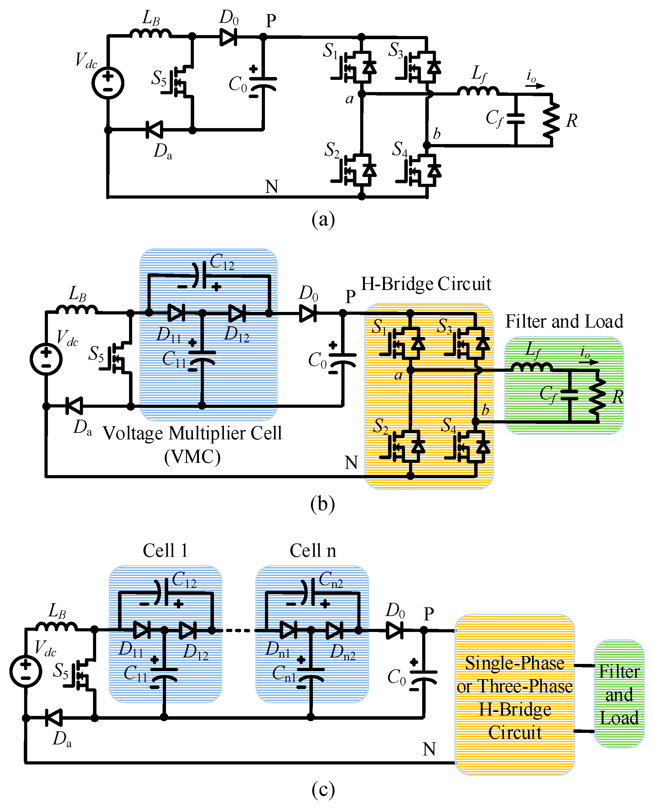
2. Proposed Inverter Topologies

The single-phase qSBI with a continuous input current [12] is presented in Figure 1a. It includes one boost inductor (LB), one capacitor (C0), six diodes (Da, D0, and four body diodes in the H-bridge circuit), five active switches (S1S5), a passive filter (Lf and Cf), and a resistive load (R). The qSBI uses the ST mode to step-up the input voltage. The following formulas of the qSBI are obtained as given in [12].
{ V P N = V S 5 = 1 1 2 D S T V d c = B · V d c v ^ o = M · B · V d c = M 1 2 D S T V d c ,
where VPN, VS5, v ^ o , B, M, and DST are the dc-bus voltage, the voltage stress on the additional switch S5, the amplitude of the output voltage, the boost factor, the modulation index, and the ST duty cycle, respectively.
From Equation (1), it can be seen that the voltage gain of the qSBI is low because DST ≤ (1–M). Moreover, the voltage stress on the additional switch S5 is high because it equals the dc-link voltage. Therefore, the qSBI is not suitable for high voltage gain applications.
Figure 1b shows the proposed single-phase VMC-qSBI with a single VMC, where two capacitors (C11 and C12) and two diodes (D11 and D12) are added to the switched-boost network. The proposed single-VMC-qSBI uses one boost inductor (LB), three capacitors (C0, C11, and C12), eight diodes (Da, D0, D11, D12, and four body diodes in the H-bridge circuit), five active switches (S1S5), a passive filter (Lf and Cf), and a resistive load (R). A combination of C11C12D11D12S5 plays a role as a VMC. It should be noted that the proposed single-VMC-qSBI will become the 2-cell SC-qSBI in [23] if the negative node of C0 is connected to the positive node of C11 in Figure 1b. Like other VMC-based converters, the proposed inverter has high current transients of the capacitor across S5, D11, D12, and D0. To reduce the current transients of capacitors and achieve soft-switching operation, a resonant inductor can be used, as reported in [24] and [25]. Figure 1c shows an n-cell extension of the proposed VMC-qSBI. Each VMC, including two capacitors and two diodes, is connected in cascade to obtain an n-cell topology. When n > 1, a multiple of two capacitors and two diodes is added to the proposed inverter. Consequently, the size, weight, and loss of the proposed inverter are increased. Note that, a three-phase H-bridge circuit can be used in the proposed converter for the three-phase inverter system.

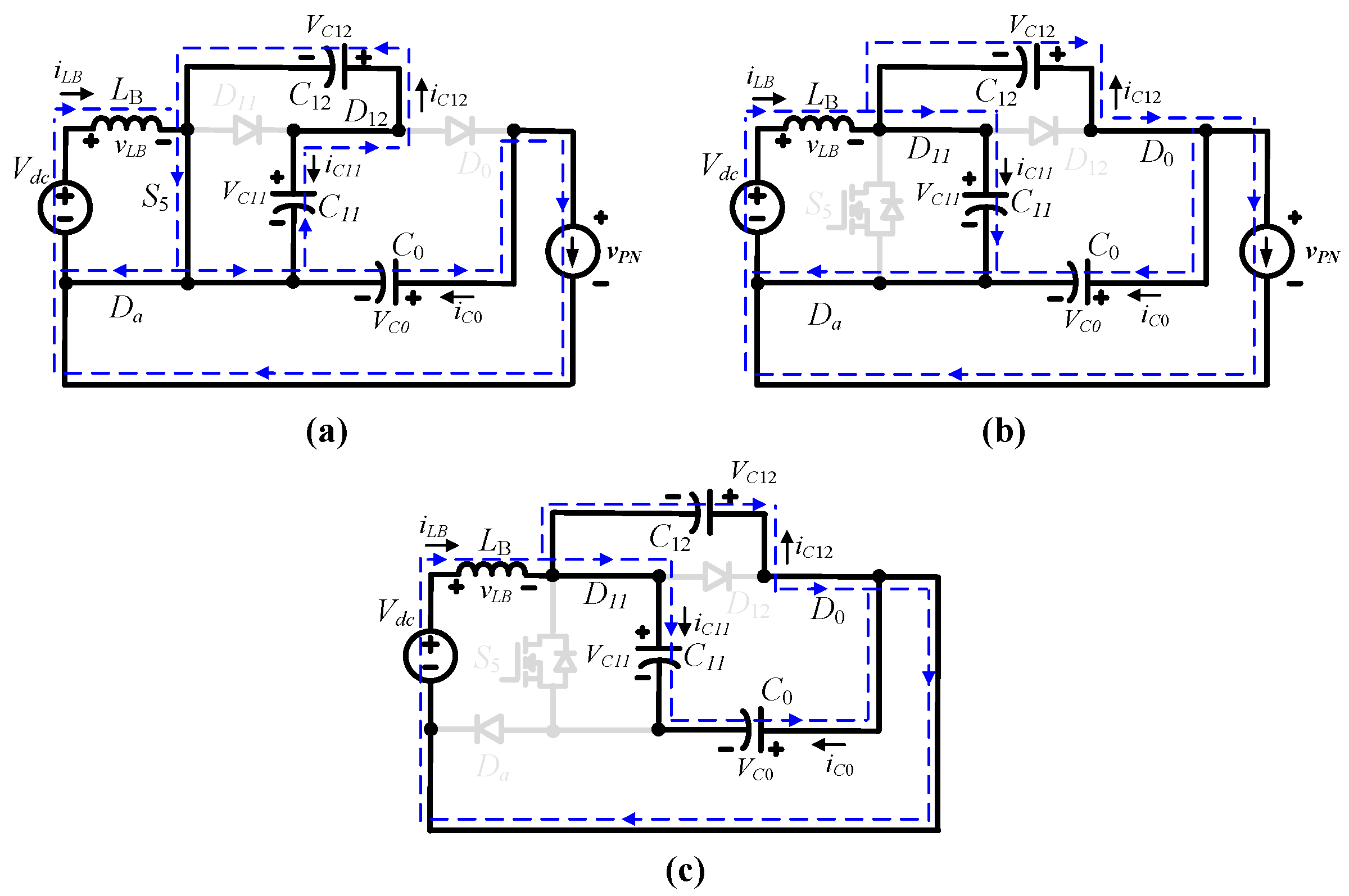
2.1. Operating States

As an example, the operating principle and steady-state analysis of the proposed single-phase single-VMC-qSBI are presented in this paper. Figure 2 shows the three operating states of the proposed single-phase single-VMC-qSBI. In the non-ST states, as shown in Figure 2a,b, the H-bridge circuit and the load side are equivalent to a current source. When the switch S5 is turned on, diodes D11 and D0 are reversed-biased, while the diodes Da and D12 are forward-biased. The inductor LB and the capacitor C12 are charged, while the capacitors C11 and C0 are discharged. The inverter operates in the non-ST state 1, as shown in Figure 2a. The time interval in the non-ST state 1 is D5·T, where D5 is the duty cycle of the switch S5 during one switching period, T. The following equations can be written as
{ L B d i L B d t = V d c V C 11 = V C 12 V P N = V C 0 a n d { C 11 d v C 11 d t = i C 12 _ N o n 1 C 12 d v C 12 d t = i C 12 _ N o n 1 C 0 d v C 0 d t = I P N ,
where IPN and iC12_Non1 are the average dc-link current and the instantaneous current through capacitor C12 in the non-ST state 1.
When the switch S5 is turned off and the H-bridge circuit generates the active or zero vectors and the inverter operates in the non-ST state 2, as shown in Figure 2b. During this state, diode D12 is reversed-biased, while the diodes Da, D11, and D0 are forward-biased. Inductor LB and capacitor C12 are discharged, while capacitors C11 and C0 are charged. The following formulas can be obtained as
{ L B d i L B d t = V d c V C 11 V C 0 = V P N = V C 11 + V C 12 and { C 11 d v C 11 d t = I L B + i C 12 _ N o n 2 C 12 d v C 12 d t = i C 12 _ N o n 2 C 0 d v C 0 d t = I P N i C 12 _ N o n 2 ,
where iC12_Non2 is the instantaneous current through capacitor C12 in the non-ST state 2.
In the ST state, as shown in Figure 2c, the H-bridge circuit is shorted by the switches on the same H-bridge leg. Meanwhile, switch S5 is turned off during the ST state. Diodes D11 and D0 are forward-biased, while diodes Da and D12 are reversed-biased. The time interval is DST·T. The inductor LB and capacitor C11 are charged, while the capacitors C12 and C0 are discharged. The following equations can be obtained as
{ L B d i L B d t = V d c + V C 12 V C 0 = V C 11 + V C 12 V P N = 0 and { C 11 d v C 11 d t = I L B + i C 12 _ S T C 12 d v C 12 d t = i C 12 _ S T C 0 d v C 0 d t = I L B i C 12 _ S T ,
where iC12_ST is the instantaneous current through capacitor C12 in the ST state.

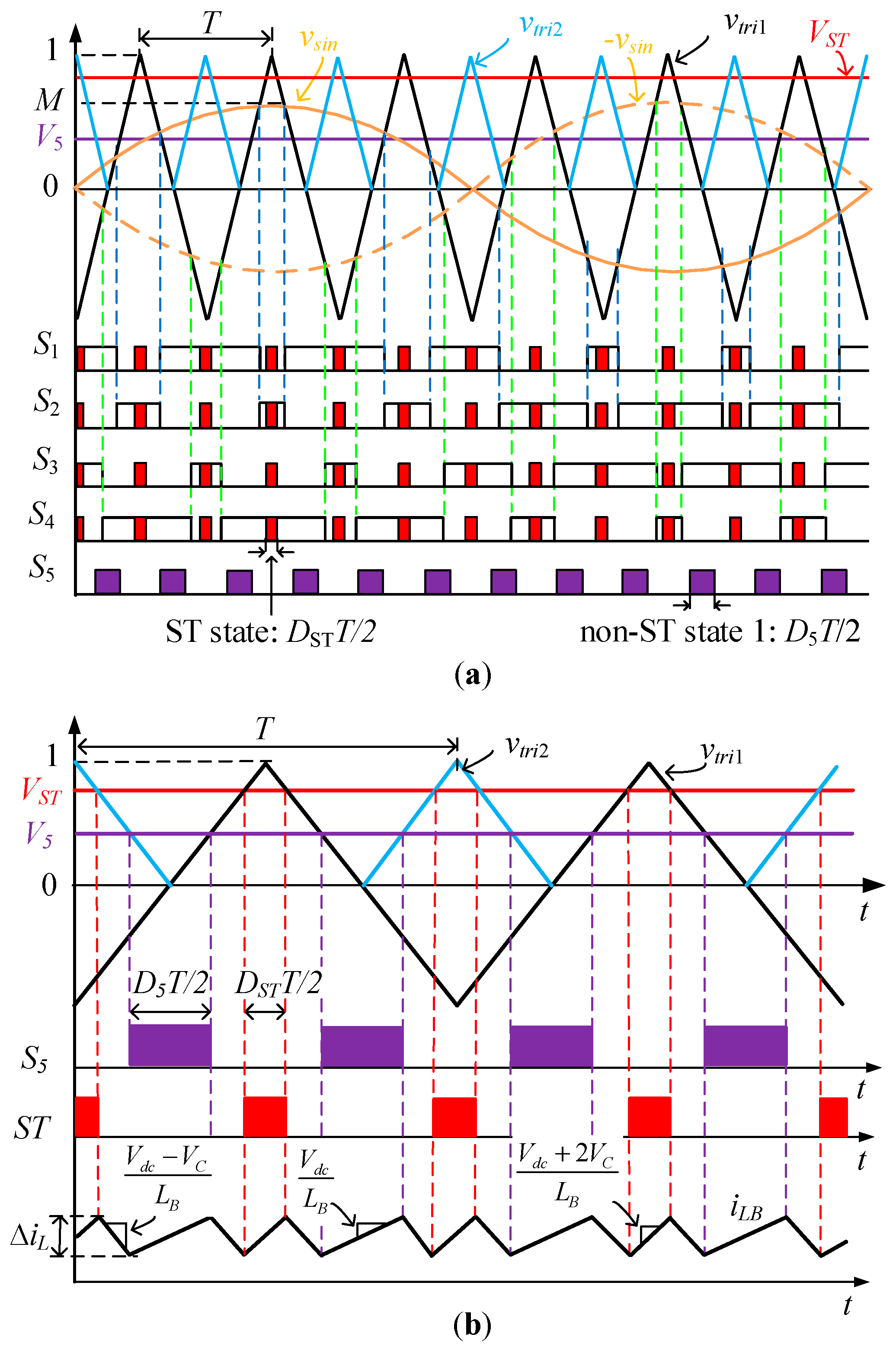
2.2. PWM Technique with Low Input Current Ripple

Figure 3 shows a PWM control technique for the proposed single-phase VMC-qSBI. As shown in Figure 3a, two sinusoidal voltages—vsin and –vsin—are compared to a high-frequency triangle waveform, vtri1, to produce PWM signals for the H-bridge switches (S1S4). A fixed voltage, V5, is compared to the triangle waveform (vtri2) with the double frequency of vtri1, as shown in Figure 3, to produce the control signal for the switch S5. To produce an ST control signal, another fixed voltage, VST, is also compared to vtri2. This ST control signal (ST in Figure 3b) is then inserted into the H-bridge switches through OR logic gates.

2.3. Steady-State Analysis

By using the volt-second balance to the inductor LB, in steady-state, from Equations (2) to (4), the voltage on the capacitors is calculated as
{ V C = V C 11 = V C 12 = 1 1 2 D S T D 5 V d c V C 0 = 2 V C = 2 1 2 D S T D 5 V d c .
Applying the charge-second balance principle to the capacitors C11, C12, and C0, from Equations (2) to (4), the following equations are obtained as Equation (6).
{ D 5 i C 12 _ N o n 1 + ( 1 D S T D 5 ) i C 12 _ N o n 2 + D S T i C 12 _ S T + ( 1 D 5 ) I L B = 0 D 5 i C 12 _ N o n 1 + ( 1 D S T D 5 ) i C 12 _ N o n 2 + D S T i C 12 _ S T = 0        ( 1 D S T D 5 ) i C 12 _ N o n 2 D S T i C 12 _ S T D S T I L B ( 1 D S T ) I P N = 0.
Solving Equation (6), the instantaneous current through capacitor C12 in the non-ST state 1 and the average inductor L1 current are given as
{ i C 12 _ N o n 1 = 1 D 5 2 D 5 I L B I L B = 2 ( 1 D S T ) 1 2 D S T D 5 I P N .
The inductor is charged during both non-ST state 1 and ST state. From Equations (2) and (4), the inductor current ripple can be rewritten as follows.
{ Δ I L _ N S T 1 = V d c L B D 5 T 2 Δ I L _ S T = V d c + V C L B D S T T 2 .
From Equation (8), it can be seen that the slope of the inductor current in the ST state is higher than that in the non-ST state 1. The inductor current ripple depends on the ST duty cycle. Further, the inductance selection is based on the maximum ST duty cycle. If we select D5 = DST or 2DST, the high-frequency (HF) inductor current ripple is too high, and the voltage gain of the inverter is not high at a high modulation index. In this paper, we select D5 = 3DST to obtain a low inductor current ripple with a high voltage gain. Substituting D5 = 3DST in to Equation (5), the peak dc-link voltage in the non-ST states is
V P N = V C 0 = 2 V C = 2 1 5 D S T V d c .
The boost factor of the proposed VMC-qSBI is calculated as
B = V P N V d c = 2 1 5 D S T .
The peak ac voltage is defined as
v ^ o = M B V d c = 2 M 1 5 D S T V d c .
For the proposed n-cell VMC-qSBI, as shown in Figure 1c, the capacitor voltage is determined in the steady-state as
{ V C = V C 11 = V C n 2 = V d c 1 ( n + 1 ) D S T D 5 V C n 1 = n V C V C 0 = ( n + 1 ) V C = ( n + 1 ) V d c 1 ( n + 1 ) D S T D 5 .
The peak ac voltage of the n-cell VMC-qSBI is expressed as
v ^ o = ( n + 1 ) M 1 ( n + 1 ) D S T D 5 V d c .

3. Parameter Design Guideline

For the single-phase inverter, there will be a pulsating power at double the fundamental frequency, which will pose a significant challenge to the front-end boost converter. Similar to other single-phase inverter topologies, the proposed single-phase VMC-qSBI also generates the double fundamental frequency ripple at the dc side. The double fundamental frequency ripple on the inductors and capacitors at the dc side can be mitigated by using a feedback control method, as reported in [10] for qZSI and [22] for qSBI. Therefore, in this study, the effect of the pulsating power can be ignored in the design stage. Then, the inductance and capacitance are only selected according to the HF ripple. The ac side circuit of the proposed VMC-qSBI is described by its equivalent dc load [12]. The average dc-link current depends on the equivalent dc load (Rl), and is calculated as [12]
I P N = ( 1 D S T ) V P N R l .

3.1. Parameter Design of Inductor

The inductor current waveform of the proposed VMC-qSBI is shown in Figure 3b. The peak-to-peak current ripple of the inductor LB is calculated as Equation (8). To limit the peak-to-peak inductor current ripple by rLB%·ILB, the inductance of L1 should be
L 1 > 3 D S T ( 1 5 D S T ) 2 R l 8 r L B % ( 1 D S T ) 2 f ,
where f = 1/T is the switching frequency of the inverter.

3.2. Parameter Design of Capacitor

To select the C11, C12, and C0 capacitances of the proposed VMC-qSBI, the peak-to-peak capacitor voltage ripples can be rewritten from Equation (2) as
{ Δ V C 11 = i C 12 _ n o n 1 C 11 · D 5 T 2 Δ V C 12 = i C 12 _ n o n 1 C 12 · D 5 T 2 Δ V C 0 = I P N C 0 · D 5 T 2 ,
Substituting Equations (6) and (14) into Equation (16), the C11, C12, and C0 capacitances of the proposed VMC-qSBI are calculated as
{ C 11 = C 12 = 2 ( 1 3 D S T ) ( 1 D S T ) 2 r C 1 % ( 1 5 D S T ) R l f C 0 = 3 D S T ( 1 D S T ) 2 r C 0 % R l f ,
where rC1% and rC0% are the voltage ripple percentages of capacitors C11 and C12 and capacitor C0, respectively.

3.3. Parameter Design of Switches

From Figure 3, the voltage stress of the diodes is calculated as
{ V S 1 S 4 = V C 0 = 2 V d c 1 5 D S T V S 5 = V C 11 = V d c 1 5 D S T .
Because the ST state turns on all of the H-bridge switches S1S4, as shown in Figure 2c, the peak current of switches S1S4 equals a half of the ST current, which is the inductor current. Consequently, the current stress of the switches S1S4 is
I S 1 S 4 = I L B 2 = 2 ( 1 D S T ) 2 ( 1 5 D S T ) 2 V d c R l .
The peak current of switch S5 is determined based on the non-ST state 1 in Figure 2a as
I S 5 = I L B + i C 12 _ N o n 1 = 2 ( 1 + 3 D S T ) ( 1 D S T ) 2 3 D S T ( 1 5 D S T ) 2 V d c R l .

3.4. Parameter Design of Diodes

From Figure 2, the voltage stress of the switches is calculated as
{ V D 0 = V D 11 = V D 12 = V C 11 = V d c 1 5 D S T V D a = V C 0 = 2 V d c 1 5 D S T .
The peak current of the diodes D0, D11, and Da should be selected such that it equals the inductor LB current, and the peak current of the diode D12 equals the instantaneous current through capacitor C12 in the non-ST state 1. Therefore, the peak current of the diodes is calculated as
{ I D a = I D 0 = I D 11 = I L B = 4 ( 1 D S T ) 2 ( 1 5 D S T ) 2 V d c R l I D 12 = i C 12 _ N o n 1 = 2 ( 1 3 D ) ( 1 D S T ) 2 3 D ( 1 5 D S T ) 2 V d c R l .

4. Comparison with Other Active Impedance Source Inverters

In this section, the proposed VMC-qSBI is compared with other active impedance source inverters. The selected topologies for comparison are the qSBI [12], the SL-qSBI [14], the SZSI [17], ASC-qZSI [19], and 2-cell SC-qSBI [23]. Table 1 shows the overall comparison between the proposed VMC-qSBI and other active impedance source inverters.

4.1. Input Current Ripple

As shown in Table 1, the input current ripple of the SL-qSBI is very high because the input current is either the inductor current in the non-ST state or the twofold inductor current in the ST state. Note that as shown in Figure 3, the PWM control method cannot be applied to the SL-qSBI [13], ASC-qZSI [19], and 2-cell SC-qSBI [23] because of the increasing harmonic distortion of the output voltage. Therefore, the input current ripple of these inverters is high. Under the same PWM control method, as shown in Figure 3, the qSBI [11], SZSI [17], and the proposed inverter have a low input current ripple.

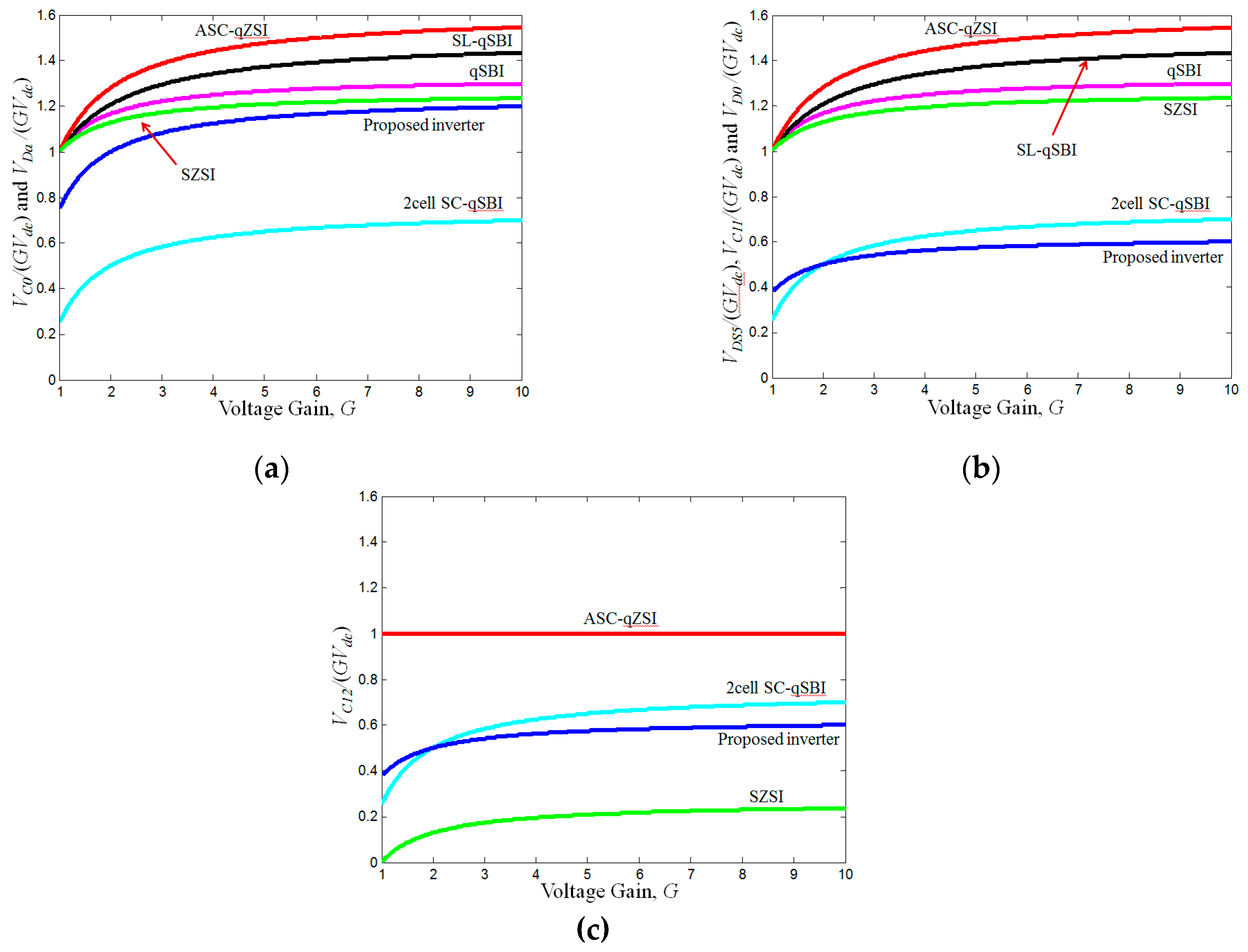
4.2. Voltage and Current Stresses

Figure 4 shows the respective ratios of the voltage stress to the equivalent dc voltage under the same PWM control method. As shown in Figure 4a, the voltage stress on capacitor C0 and diode Da of the proposed VMC-qSBI is higher than that of the 2-cell SC-qSBI. However, the voltage stress on switch S5, capacitors C11 and C0, and diodes D0 and Da of the proposed VMC-qSBI are smaller than that of the other active impedance source inverters, as shown in Figure 4a,b. The capacitor C12 voltage stress of the proposed VMC-qSBI is smaller than that of the ASC-qZSI and 2-cell SC-qSBI, but it is higher than that of SZSI.
The inductor current stress comparison is shown in Figure 5a. Because the qSBI, ASC-qSBI, 2-cell SC-qSBI, and the proposed VMC-qSBI have a single inductor, their inductor current stress is highest and is equal to the source current. Figure 5b shows the ST current stress comparison. The proposed VMC-qSBI, qSBI, and 2-cell SC-qSBI have the lowest ST current stress.

4.3. Voltage Gain and Boost Factor

Figure 5c,d compares the boost factor and the voltage gain of the proposed VMC-qSBI with those of the active impendence source inverters, respectively. The voltage gain of the proposed VMC-qSBI is greatest for the same modulation index. The high modulation index is very important to achieve a high output waveform quality with a low total harmonic distortion (THD).

4.4. Element Count

Table 1 also compares the number of elements required for the inverters. Although the proposed VMC-qSBI adds one active switch, it results in savings of a large number of passive devices compared with the high voltage gain qZSIs in [17,19,20]. The proposed VMC-qSBI has the same number of semiconductors as the SZSI, but it uses one more capacitor and one less inductor. Compared with the SL-qSBI, the proposed VMC-qSBI uses two more capacitors, one less diode, and one less inductor. The proposed inverter uses the same number of components as the 2-cell SC-qSBI. Note that the number of diodes in Table 1 includes four body diodes of the H-bridge switches.

5. Simulation and Experiment Results

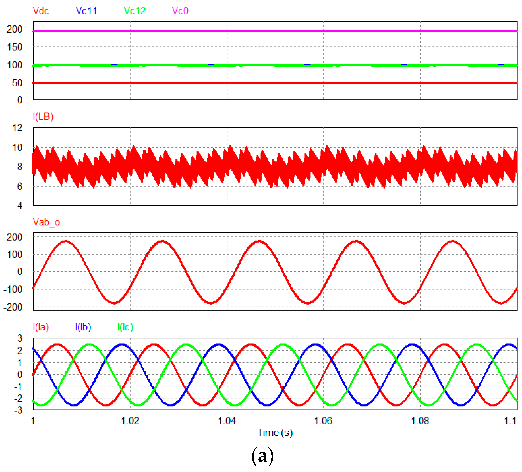
5.1. Simulation Results

To validate the performance of the proposed inverter, PSIM simulation software was used. The simulation parameters for the single-phase VMC-qSBI are given in Table 2. The drain-to-source on-resistance of the switches S1S4 and the switch S5 was set to 0.2 Ω and 8 mΩ, respectively. The body diode threshold voltage of the switches S1S4 and the forward voltage of the diodes Da, D0, D11, and D12 are 1.5 V and 0.73 V, respectively. The fundamental frequency of the ac output voltage and the switching frequency are 50 Hz and 20 kHz, respectively. An inductor-capacitor (LC) filter of 1 mH and 20 µF was connected to the inverter output. A purely resistive load of 40 Ω was used in the simulation.
Figure 6 shows the simulation results for the single-phase VMC-qSBI when Vdc = 50 V, DST = 0.1, D5 = 0.3, and M = 0.9. Because of the existing passive components in the impedance-source network, an inrush current has appeared at the start-up process, as can be seen in Figure 6a. Figure 6b,c shows the simulation results in the steady-state. The voltage of capacitors C11, C12, and C0 in the steady-state are boosted to 97.1 V, 96.2 V, and 193 V, respectively. The ac output voltage is 121 Vrms. The input current is continuous and has a small peak-to-peak ripple of 0.92 A.
The three-phase VMC-qSBI as shown in Figure 7 is used to test the PWM technique with low input current ripple as presented in Section 2.2. All parameters of the three-phase VMC-qSBI including capacitance, inductance, diodes, MOSFETs, and load are the same as those of the single-phase VMC-qSBI. The maximum constant boost PWM control method in [28] is used to control three-phase H-bridge switches, while the additional switch S5 is controlled by the constant voltage V5 as shown in Figure 3b. Figure 8 shows the simulation results for the three-phase VMC-qSBI when Vdc = 50 V, DST = 0.1, D5 = 0.3, and M = 0.9 × 1.15. As shown in Figure 8a, the capacitors C11, C12, and C0 voltage are boosted to 98 V, 97 V, and 195 V in the steady-state, respectively. The three phase currents are 1.8 A in RMS. Under resistive load of 40 Ω, the simulated output phase voltage is 72 V in RMS, whereas the calculated value of the output phase voltage is 73 V in RMS. The input current is continuous. As shown in Figure 6b and Figure 8b, the Da diode reverse voltage is zero in non-ST states, and is equal to capacitor C0 voltage in the ST state. The voltage stress on the additional switch S5 is a half of dc-link voltage. All of the simulation results are in agreement with the theoretical analysis.

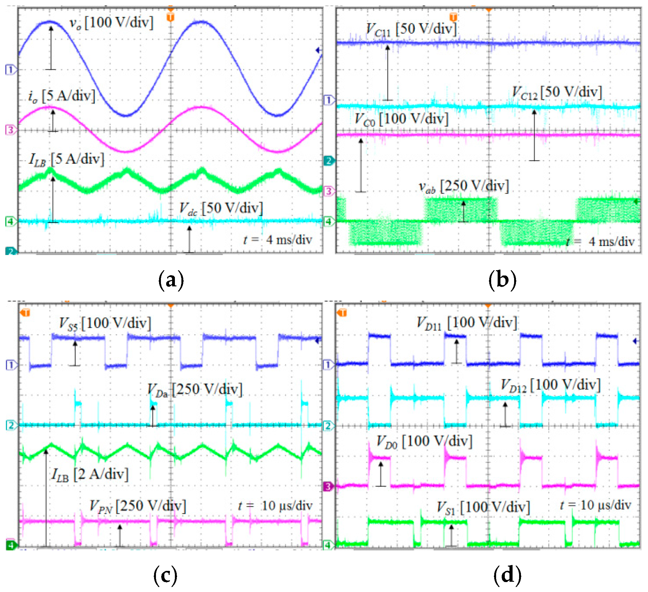
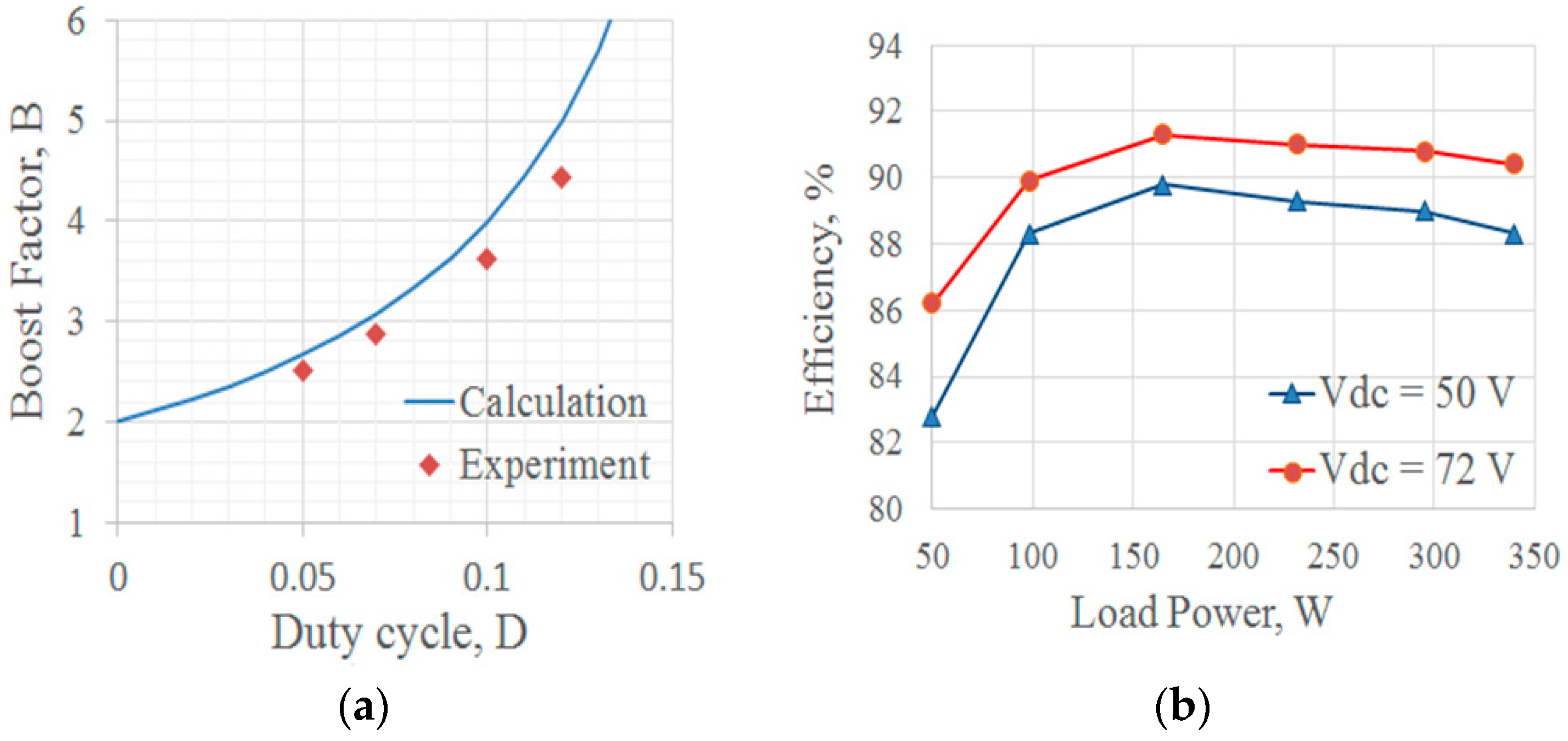
5.2. Experimental Results

The experimental prototype was built to test the proposed VMC-qSBI. A 0.37 mH boost inductor was used, and the dc input voltage is supplied by 61604 Chroma Programmable ac Sources with a current limit of 8 A. The voltage stress on switch S5 is equal to the capacitor C11 and C12 voltages; thus, for switch S5, the IRFP4668 MOSFET was chosen with a voltage limit of 200 V. The switches on the H-bridge circuit are IRFP460 MOSFETs. Three diodes D11, D12, and D0 are Schottky STPS60SM200C diodes, and one IXYS30-60A is used as the diode Da. Capacitors C11 and C12 are 1000 µF/100 V. The capacitor C0 was obtained by connecting in parallel two 680 µF/200 V capacitors. The parameters of the experiment are listed in Table 2. The switching frequency of the H-bridge switches is 20 kHz, and the switching frequency of switch S5 is 40 kHz. The PWM control signals of the switches are generated by TMS320F28335 DSP, and are driven by isolated TLP250 amplifiers.
Figure 9 shows the experimental results of the proposed VMC-qSBI when Vdc = 50 V, M = 0.9, Vo = 110 Vrms, and Po = 300 W. The dc-link voltage is boosted to 181 V from the input voltage of 50 V. The voltages of capacitors C11, C12, and C0 are boosted to 91.6 V, 89.7 V, and 181 V, respectively, in the steady-state. The boost factor of the experiment is 3.62, while the calculated value for DST = 0.1 from Equation (10) in the ideal case is 4. The ac output voltage is 110 Vrms/50 Hz. The input current is continuous. The current THD at the output is 0.9%. The HF peak-to-peak inductor current of 1.1 A is presented in Figure 9c.
Then, the input voltage is increased to 72 V. To obtain the same 110-Vrms output voltage while the modulation index is kept at 0.9, the ST duty cycle is decreased to 0.05. Figure 10 shows the experimental results of the VMC-qSBI when Vdc = 72 V, M = 0.9, Vo = 110 Vrms, and Po = 300 W. The voltages of capacitors C11, C12, and C0 are boosted to 91.2 V, 90.2 V, and 181 V, respectively, from a 72 V input voltage. The HF peak-to-peak inductor current is 0.8 A. The measured THD of the output current is 1%.
Figure 11a,b shows the gate-pulse waveforms for switches S1S3 when Vdc is 50 V and 72 V, respectively. As shown in Figure 11a,b, the overlap duty cycle (DST) of the gate pulse for switches S1S3 is one-third of the duty cycle of switch S5. The waveforms from top to bottom in Figure 9a and Figure 10a are the output voltage after the L-C filter, the load current, the input current, and the input voltage. The waveforms from top to bottom in Figure 9b and Figure 10b are the voltages across capacitors C11, C12, and C0, and the output voltage before the L-C filter. The waveforms from top to bottom in Figure 9c and Figure 10c are the drain-source S5 voltage, the diode Da voltage, the input current, and the dc-link voltage. The waveforms from top to bottom in Figure 9d and Figure 10d are the voltages across diodes D11, D12, and D0, and the drain-source S1 voltage. The waveforms in Figure 11a,b are the control gate signals of S5 and S1S3.
Figure 12a shows the boost factor comparison between the calculation and the experiment for the VMC-qSBI. In this experiment, the duty cycle was varied from 0.05 to 0.12, while the output voltage and the output power were kept at 110 Vrms and 300 W, respectively. Because of the parasitic elements in the experimental setup, the experimental values are lower than the calculated values. Figure 12b shows the efficiency of the VMC-qSBI with various power loads. The maximum efficiency value of the VMC-qSBI at a load power of 165 W and an input voltage of 72 V is 91.3%.

6. Discussions and Conclusion

Although ZS/qZSIs and qSBIs have a good performance with buck-boost voltage function, single-stage conversion, and ST immunity, their disadvantage is high voltage stress on capacitors, diodes, and switch. Using a small voltage rating of the devices leads to reduce the loss and cost of the power inverter system. Moreover, a small ST duty ratio or a high modulation index helps to enhance the output waveform quality of the inverter. In this paper, a new single-phase single-stage boost inverter based on the VMC structure was proposed. A new PWM control strategy was used for the proposed inverter to achieve a high voltage gain with a low input current ripple. Compared to the other active impedance source inverters, the proposed VMC-qSBI has a high voltage gain, low input current ripple, low voltage stress on the switch and diode, low ST current, and high modulation index. The extension was presented to improve the voltage gain of the proposed inverter by adding the VMCs. The operating modes, steady-state analysis, and design guideline were presented. A laboratory prototype was tested to verify the accuracy of the proposed VMC-qSBI. Simulation and experimental results were shown.
Because the proposed VMC-qSBI has high reliability with ST immunity, low voltage stress on devices, and high voltage gain inversion with multi-VMCs, it is suitable for renewable energy system applications such as photovoltaic and wind power.

Author Contributions

M.-K.N. conducted topology, experimental work, data analysis, and writing the original draft. Y.-O.C. reviewed and revised the whole work.

Funding

This research was funded by the Korea Institute of Energy Technology Evaluation and Planning (KETEP) and the Ministry of Trade, Industry& Energy (MOTIE) of the Republic of Korea grant number 20184010201650 and the APC was funded by KETEP and MOTIE.

Acknowledgments

This work was supported by the Korea Institute of Energy Technology Evaluation and Planning (KETEP) and the Ministry of Trade, Industry& Energy (MOTIE) of the Republic of Korea (NO. 20184010201650).

Conflicts of Interest

The authors declare no conflict of interest.

References

  1. Meneses, D.; Blaabjerg, F.; Garcıa, O.; Cobos, J.A. Review and comparison of step-up transformerless topologies for photovoltaic ac-module application. IEEE Trans. Power Electron. 2013, 28, 2649–2663. [Google Scholar] [CrossRef]
  2. Maris, T.I.; Kourtesi, S.; Ekonomou, L.; Fotis, G.P. Modeling of a single phase photovoltaic inverter. Solar Energy Mater. Sol. Cells. 2007, 91, 1713–1725. [Google Scholar] [CrossRef]
  3. Anderson, J.; Peng, F. A class of quasi-Z-source inverters. In Proceedings of the 2008 IEEE Industry Applications Society Annual Meeting, Edmonton, AB, Canada, 5–9 October 2008; pp. 1–7. [Google Scholar]
  4. Kadwane, S.G.; Shinde, U.K.; Gawande, S.P.; Keshri, R.K. Symmetrical shoot-through based decoupled control of Z-source inverter. IEEE Access. 2017, 5, 11298–11306. [Google Scholar] [CrossRef]
  5. Nguyen, M.K.; Lim, Y.C.; Choi, J.H. Two switched-inductor quasi-Z-source inverters. IET Power Electron. 2012, 5, 1017–1025. [Google Scholar] [CrossRef]
  6. Nguyen, M.K.; Lim, Y.C.; Cho, G.B. Switched-inductor quasi-Z-source inverter. IEEE Trans. Power Electron. 2011, 26, 3183–3191. [Google Scholar] [CrossRef]
  7. Jagan, V.; Kotturu, J.; Das, S. Enhanced-boost quasi-Z-source inverters with two-switched impedance networks. IEEE Trans. Ind. Electron. 2017, 64, 6885–6897. [Google Scholar] [CrossRef]
  8. Ho, A.V.; Chun, T.W. Modified capacitor-assisted Z-source inverter topology with enhanced boost ability. J. Power Electron. 2017, 17, 1195–1202. [Google Scholar]
  9. Qian, W.; Peng, F.Z.; Cha, H. Trans-Z-source inverters. IEEE Trans. Power Electron. 2011, 26, 3453–3463. [Google Scholar] [CrossRef]
  10. Ge, B.; Liu, Y.; Abu-Rub, H.; Balog, R.S.; Peng, F.Z.; McConnell, S.; Li, X. Current ripple damping control to minimize impedance network for single phase quasi-Z source system. IEEE Trans. Ind. Informat. 2016, 12, 1054–4848. [Google Scholar] [CrossRef]
  11. Mishra, S.; Adda, R.; Joshi, A. Inverse Watkins–Johnson topology-based inverter. IEEE Trans. Power Electron. 2012, 27, 1066–1070. [Google Scholar] [CrossRef]
  12. Nguyen, M.K.; Le, T.V.; Park, S.J.; Lim, Y.C. A class of quasi-switched boost inverters. IEEE Trans. Ind. Electron. 2015, 62, 1526–1536. [Google Scholar] [CrossRef]
  13. Nguyen, M.K.; Lim, Y.C.; Park, S.J. A comparison between single-phase quasi-Z-source and quasi-switched boost inverters. IEEE Trans. Ind. Electron. 2015, 62, 6336–6344. [Google Scholar] [CrossRef]
  14. Nguyen, M.K.; Le, T.V.; Park, S.J.; Lim, Y.C.; Yoo, J.Y. A class of high boost inverters based on switched-inductor structure. IET Power Electron. 2015, 8, 750–759. [Google Scholar] [CrossRef]
  15. Ho, A.V.; Chun, T.W.; Kim, H.G. Development of multi-cell active switched-capacitor and switched-inductor Z-source inverter topologies. J. Power Electron. 2014, 14, 834–841. [Google Scholar] [CrossRef]
  16. Chub, A.; Liivik, L.; Zakis, J.; Vinnikon, D. Improved switched-inductor quasi-switched-boost inverter with low input current ripple. In Proceedings of the 56th International Scientific Conference on Power and Electrical Engineering of Riga Technical University (RTUCON), Riga, Latvia, 14 October 2015; pp. 1–6. [Google Scholar]
  17. Nozadian, M.H.B.; Babaei, E.; Hosseini, S.H.; Asl, E.S. Steady-state analysis and design considerations of high voltage gain switched Z-source inverter with continuous input current. IEEE Trans. Ind. Electron. 2017, 64, 5342–5350. [Google Scholar] [CrossRef]
  18. Nguyen, M.K.; Duong, T.D.; Lim, Y.C.; Choi, J.H. High voltage gain quasi-switched boost inverters with low input current ripple. IEEE Trans. Ind. Informat. (Early Access) 2018, 1. [Google Scholar] [CrossRef]
  19. Ho, A.V.; Hyun, J.S.; Chun, T.W.; Lee, H.H. Embedded quasi-Z-source inverters based on active switched-capacitor structure. In Proceedings of the IECON 2016—42nd Annual Conference of the IEEE Industrial Electronics Society, Florence, Italy, 23–26 October 2016; pp. 3384–3389. [Google Scholar]
  20. Nguyen, M.K.; Lim, Y.C.; Choi, J.H.; Choi, Y.O. Trans-switched boost inverters. IET Power Electron. 2016, 9, 1065–1073. [Google Scholar] [CrossRef]
  21. Nguyen, M.K.; Tran, T.T.; Lim, Y.C. A family of PWM control strategies for single-phase quasi-switched-boost inverter. IEEE Trans. Power Electron. 2019, 34, 1458–1469. [Google Scholar] [CrossRef]
  22. Gambhir, A.; Mishra, S.K.; Joshi, A. Power frequency harmonic reduction and its redistribution for improved filter design in current-fed switched inverter. IEEE Trans. Ind. Electron. 2019, 66, 4319–4333. [Google Scholar] [CrossRef]
  23. Nguyen, M.K.; Duong, T.D.; Lim, Y.C.; Kim, Y.G. Switched-capacitor quasi-switched boost inverters. IEEE Trans. Ind. Electron. 2018, 65, 5105–5113. [Google Scholar] [CrossRef]
  24. Prudente, M.; Pfitscher, L.L.; Emmendoerfer, G.; Romaneli, E.F.; Gules, R. Voltage multiplier cells applied to non-isolated dc–dc converters. IEEE Trans. Power Electron. 2008, 23, 871–887. [Google Scholar] [CrossRef]
  25. Deng, Y.; Rong, Q.; Li, W.; Zhao, Y.; Shi, J.; He, X. Single-switch high step-up converters with built-in transformer voltage multiplier cell. IEEE Trans. Power Electron. 2012, 27, 3557–3567. [Google Scholar] [CrossRef]
  26. Alcazar, Y.J.A.; Oliveira, D.D.S.; Tofoli, F.L.; Torrico-Bascope, R.P. DC-DC nonisolated boost converter based on the three-state switching cell and voltage multiplier cells. IEEE Trans. Ind. Electron. 2013, 60, 4438–4449. [Google Scholar] [CrossRef]
  27. Berkovich, Y.; Shenkman, A.; Axelrod, B.; Golan, G. Structures of transformerless step-up and step-down controlled rectifiers. IET Power Electron. 2008, 1, 245–254. [Google Scholar] [CrossRef]
  28. Shen, M.; Wang, J.; Joseph, A.; Peng, F.Z.; Tolbert, L.M.; Adams, D.J. Constant boost control of the Z-source inverter to minimize current ripple and voltage stress. IEEE Trans. Ind. Appl. 2006, 42, 770–778. [Google Scholar] [CrossRef]
Figure 1. Conventional and proposed inverter topologies. (a) Conventional quasi-switched boost inverter (qSBI), (b) proposed single voltage multiplier cell (VMC-qSBI), and (c) proposed n-VMC-qSBI extension topologies.
Electronics 08 00227 g001
Figure 2. Operating states of proposed single-VMC-qSBI. (a) Non-ST state 1, (b) non-ST state 2, and (c) ST state.
Electronics 08 00227 g002
Figure 3. Pulse-width modulation (PWM) control technique for the proposed single-phase inverter. (a) Signal generation and (b) enlargement waveforms.
Electronics 08 00227 g003
Figure 4. Voltage stress comparison. (a) Voltage stress on capacitor C0 and diode Da, (b) voltage stress on switch S5, capacitor C11, and diode D0, and (c) capacitor C12 voltage stress.
Electronics 08 00227 g004
Figure 5. Voltage and current stress comparison. (a) Inductor current stress, (b) ST current stress, (c) boost factor, and (d) voltage gain.
Electronics 08 00227 g005aElectronics 08 00227 g005b
Figure 6. Simulation results for the proposed single-phase VMC-qSBI when Vdc = 50 V. From top to bottom: (a) input current, capacitor voltages, dc-link current, and output voltage; (b) dc-link voltage, drain-source voltage of S5, diodes DaD11 voltage, and input current; and (c) input voltage and capacitors voltages, input current, output current, and output voltages before and after the L-C filter.
Electronics 08 00227 g006
Figure 7. Proposed three-phase VMC-qSBI in simulation.
Electronics 08 00227 g007
Figure 8. Simulation results for the proposed three-phase VMC-qSBI when Vdc = 50 V, DST = 0.1, D5 = 0.3, and M = 0.9 × 1.15. From top to bottom: (a) input voltage and capacitors voltages, input current, line-to-line voltage, and output currents and (b) dc-link voltage, drain-source voltage of S5, diode Da voltage, and input current.
Electronics 08 00227 g008aElectronics 08 00227 g008b
Figure 9. Experimental waveforms for the proposed inverter when Vdc = 50 V. From top to bottom: (a) output voltage after the L-C filter, load current, input current, and input voltage; (b) voltages across capacitors C11, C12, and C0, and output voltage before the L-C filter, (c) drain-source S5 voltage, diode Da voltage, input current, and dc-link voltage; and (d) voltages across diodes D11, D12, and D0, and the drain-source S1 voltage.
Electronics 08 00227 g009
Figure 10. Experimental waveforms for the proposed inverter when Vdc = 72 V. From top to bottom: (a) output voltage after the L-C filter, load current, input current, and input voltage; (b) voltages across capacitors C11, C12, and C0, and output voltage before the L-C filter, (c) drain-source S5 voltage, diode Da voltage, input current, and dc-link voltage; and (d) voltages across diodes D11, D12, and D0, and the drain-source S1 voltage.
Electronics 08 00227 g010
Figure 11. Control signal waveforms when (a) Vdc = 50 V and (b) Vdc = 72 V.
Electronics 08 00227 g011
Figure 12. Measured results of (a) boost factor and (b) efficiency of the proposed inverter.
Electronics 08 00227 g012
Table 1. Overall comparison of the proposed VMC-qSBI and other active impedance source inverters using the same PWM method.
qSBI [12]SL-qSBI* [14]SZSI [17]ASC-qZSI* [19]2-cell SC-qSBI* [23]Single-VMC-qSBI
Boost factor (B) 1 1 4 D S T 1 + D S T 1 3 D S T 1 1 5 D S T + D S T 2 1 1 3 D S T + D S T 2 2 1 3 D S T 2 1 5 D S T
Gain voltage (G) M 4 M 3 2 M M 2 3 M 2 M M 2 + 3 M 3 M M 2 + M 1 2 M 3 M 2 2 M 5 M 4
Input current rippleLowVery highLowHighHighLow
ILB/IPN ( 1 D S T ) B ( 1 D S T ) B / ( 1 + D S T ) ( 1 D S T ) B ( 1 D S T ) B ( 1 D S T ) B ( 1 D S T ) B
IL2/IPNNA ( 1 D S T ) B / ( 1 + D S T ) ( 1 D S T ) 2 B ( 1 D S T ) 2 B NANA
IS5/IPN ( 1 D S T ) B 2 ( 1 D S T ) B 1 + D S T ( 1 D S T ) B ( 1 D S T ) B ( 1 D S T ) D S T ( 1 3 D S T ) ( 1 D S T ) ( 1 + 3 D S T ) 3 D S T ( 1 5 D S T )
ST current (Ish/IPN) ( 1 D S T ) B 2 ( 1 D S T ) B 1 + D S T ( 1 D S T ) ( 2 D S T ) B ( 1 D S T ) ( 2 D S T ) B ( 1 D S T ) B ( 1 D S T ) B
VC0/Vdc and VDa/VdcBBBBB/2B
VC11/VdcBBBBB/2B/2
VC12/VdcNANADSTB ( 1 D S T ) B B/2B/2
VDS5/Vdc and VD0/VdcBBBBB/2B/2
Switch555555
Diode698688
Inductor122211
Capacitor112233
where VDS5 is the drain-source voltage stress on S5. NA: Not applicable; *Note that the PWM control method in Figure 3 cannot be applied to these inverters.
Table 2. Parameters used for simulation and test.
ParametersValues
Input voltage range (Vdc)50–72 V
Maximum input current 8 A
Output power (Po)350 W
Output voltage (Vo)110 Vrms/50 Hz
Input inductor0.37 mH
CapacitorsC11, C121000 µF/100 V
C02 × 680 µF/200 V
Output filterLf1 mH
Cf20 µF
Switching frequency 20 kHz
Modulation index (M)0.9
MOSFETsS5IRFP4668 (200 V, 140 A)
S1~S4IRFP460 (500 V, 20 A)
DiodesD11, D12, D0STPS60SM200C (200 V, 30 A)
DaIXYS30-60A (600 V, 37 A)

