Small-Signal Stability Analysis of Multi-Terminal DC Grids


Engineering and Design Department, Electrical Engineering, Western Washington University, Bellingham, WA 98225, USA
Electronics 2019, 8(2), 130; https://doi.org/10.3390/electronics8020130
Submission received: 14 January 2019
/
Revised: 14 January 2019
/
Accepted: 21 January 2019
/
Published: 26 January 2019
(This article belongs to the Special Issue Advanced Power Conversion Technologies)
Abstract
:This paper presents a detailed small-signal analysis and an improved dc power sharing scheme for a six terminal dc grid. The multi-terminal DC (MTDC) system is composed of (1) two voltage-source converters (VSCs) entities operating as rectification stations; (2) two VSCs operating as inverting stations; (3) two dc/dc conversion stations; and (4) an interconnected dc networking infrastructure. The small-signal state-space sub-models of the individual entities are developed and integrated to formulate the state-space model of the entire system. Using the modal analysis, it is shown that the most critical modes are associated with the power sharing droop coefficients of the rectification stations, which are constrained by the steady-state operational requirements. Therefore, a second degree-of-freedom compensation scheme is proposed to improve the dynamic response of the MTDC system without influencing the steady-state operation. Time domain simulation results are presented to validate the analysis and show the effectiveness of the proposed techniques.
1. Introduction
Following the progressive improvements in the semiconductors industry, high-voltage-high-power power electronic converters are recently emerging the market. The newly developed ABB HiPak™ insulated-gate-bipolar-transistor (IGBT) is introduced with high power density (4.5 kV, 1.2 kA) and a relatively high switching frequency of 2 kHz [1]. Motivated by these improvements, voltage-source converters (VSC)-based HVDC systems are widely adopted [2]. VSCs have recently reached a dc voltage level of 350 kV whereas the largest installed dc transmission system is rated at 400 MW [3]. Futuristic visions of multi-terminal dc (MTDC) grids are investigated to evaluate their cost-benefit feasibility. As compared to point-to-point HVDC systems, MTDC grids are technically well-suited to interface scattered-long-distant bulk delivery of offshore wind energy [3,4].
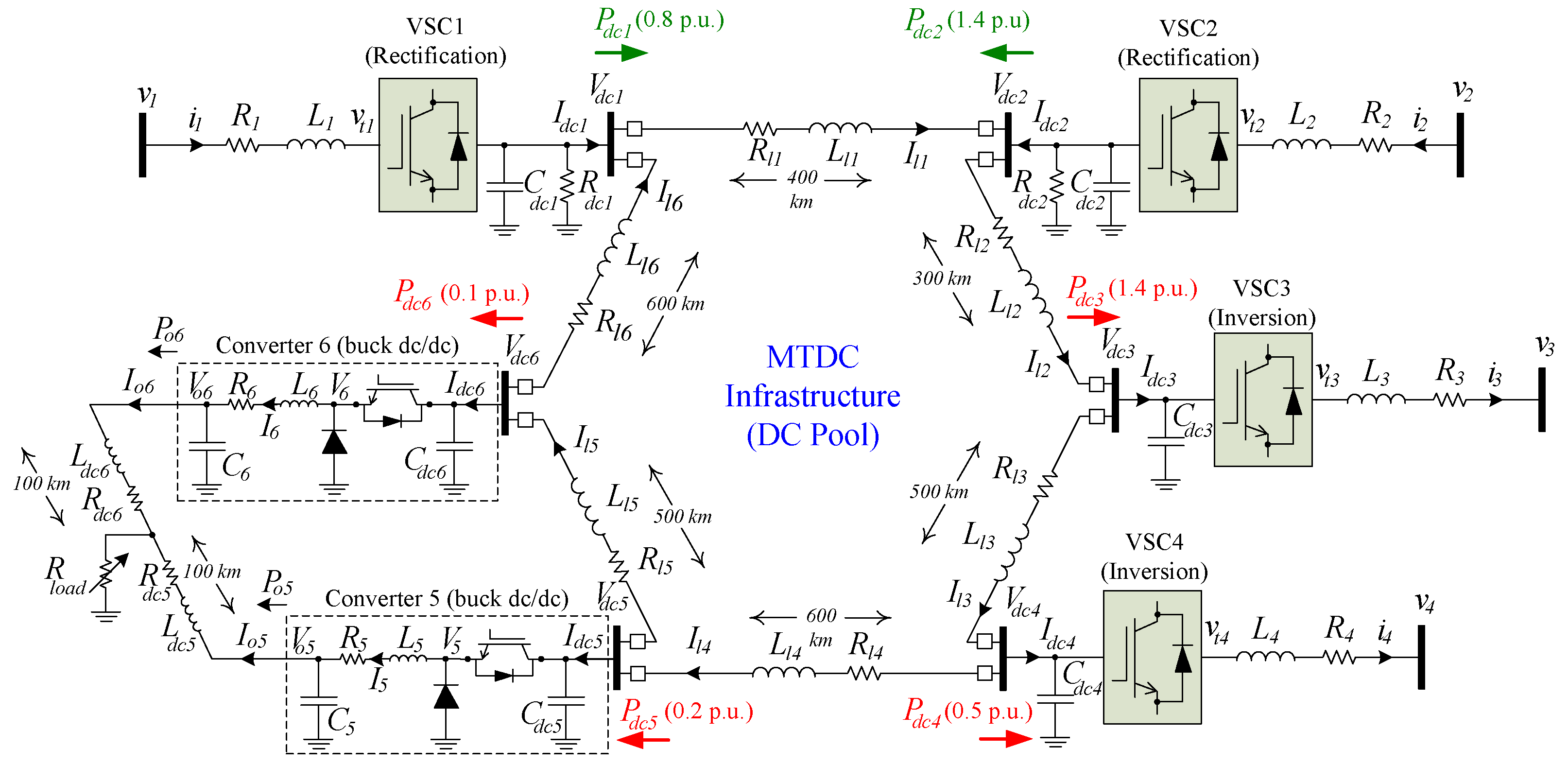
In the future power systems, dc grids (among them, the MTDC) are expected to penetrate the ac power system to interconnect multiple ac networks, express infeed systems to city centers or supply remote areas [5,6,7]. As shown in Figure 1, the MTDC system understudy is an adapted version from [6] and is formed to interface six power electronic-based entities [6,7]. The MTDC infrastructure can be considered as a dc pool that supplies/receives dc powers to/from the terminal entities. The rectification stations consist of voltage-source rectifiers (VSRs), denoted as VSC1 and VSC2 in Figure 1, which operate as supplying units to inject the dc powers ( and ) to the dc pool. The ac sides of VSC1 and VSC2 can be wind or photovoltaic farms, or a remotely-connected ac utility-grid. On the same figure, there are four loading entities: Two are interfaced by voltage-source inverters (VSIs), denoted as VSC3 and VSC4, to supply the dc power ( and ) to the remotely-connected ac grids whereas two dc/dc buck converters draw and in order to share a common resistive load (). The base value of the dc power and the dc voltage for the MTDC system in Figure 1 are and , respectively.
In literature, the control of the MTDC systems is categorized into two main schemes: The master-slave and the dc-voltage droop control scheme. The reliability of the master-slave configuration is relatively low because the loss of the master converter is followed by an immediate failure of the entire system. Moreover, the master converter broadcasts the control commands to the slave converters via communication means, which might not be a feasible option in the remotely dispersed MTDC networks [8]. On the contrary, the dc-voltage droop control offers a much higher reliability because the operation of the MTDC network is not dependent on one converter and the control strategy is entirely autonomous [9].
A systematic control design procedure and a stability analysis for a MTDC system connecting offshore wind farms to ac systems have been presented in [10]. The authors emphasize on the droop selection criteria and use a behavioral model of VSCs, which does not reflect the complete dynamics of the overall system. A dc droop-based control scheme has been considered in [11] where the droop controllers are designed by solving a convex optimization problem with linear matrix inequalities. Another work in [12] investigates the influence of the transmission-lines resistance within the MTDC network in the steady-state conditions using static power flow tools. However, the associated dynamic stability conditions are not addressed.
A modified droop control loop has been proposed in [13,14] to provide a frequency support to the interconnected ac grids via the MTDC network. The modified droop scheme is effective in reducing the frequency deviations following disturbances on the ac side. An adaptive droop control scheme is provided in [15] to ensure a proper distribution of the power burden among the droop-equipped converters. In [16], a small-signal stability study of the MTDC network is conducted considering the dynamics of the interconnected ac machines. However, the influence of the droop-based power sharing is not addressed. Multiple simulation results are shown in [17] to reflect the effectiveness of the MTDC networks as an attractive transmission system.
Motivated by the potential benefits of the high-voltage dc networks, this paper presents an extensive modal analysis based on a complete state-space model for the MTDC system shown in Figure 1. The influence of the droop-based dc power sharing control on the MTDC system stability is investigated. It is shown that the high dc-voltage droop coefficients have a positive influence on the system stability but is accompanied with a remarkable steady-state degradation in the dc-voltage regulation. On the contrary, the small droop coefficients reflect a better dc-voltage regulation at the expense of the system stability. A coupling between the dynamic performance and the steady-state operation is therefore yielded (a trade-off). In this paper, a second degree-of-freedom is proposed and implemented in the control structure of the VSCs in order to separate the coupling between the dynamic and the steady-state performance.
The contributions of this paper are as following:
- -
- The development of the detailed and accurate small-signal modeling of the MTDC system in Figure 1.
- -
- Conducting the stability and sensitivity analysis to investigate the influence of the parameters variations on the system stability.
- -
- Implementing the proposed dynamic droop loops to enhance the system stability without affecting the steady-state performance.
- -
- Conducting time-domain simulations using Matlab/Simulink for the entire MTDC system.
2. Large-Signal Model of the MTDC System
The MTDC system under study is shown in Figure 1. The following subsections detail the large-signal modeling of the MTDC entities.
2.1. Rectification Stations 1-2
As shown in Figure 1, the power circuit of the ac side of VSC1 is modelled in the rotating - reference frame as shown in (1), whereas the model of the dc-link capacitor is shown in (2).
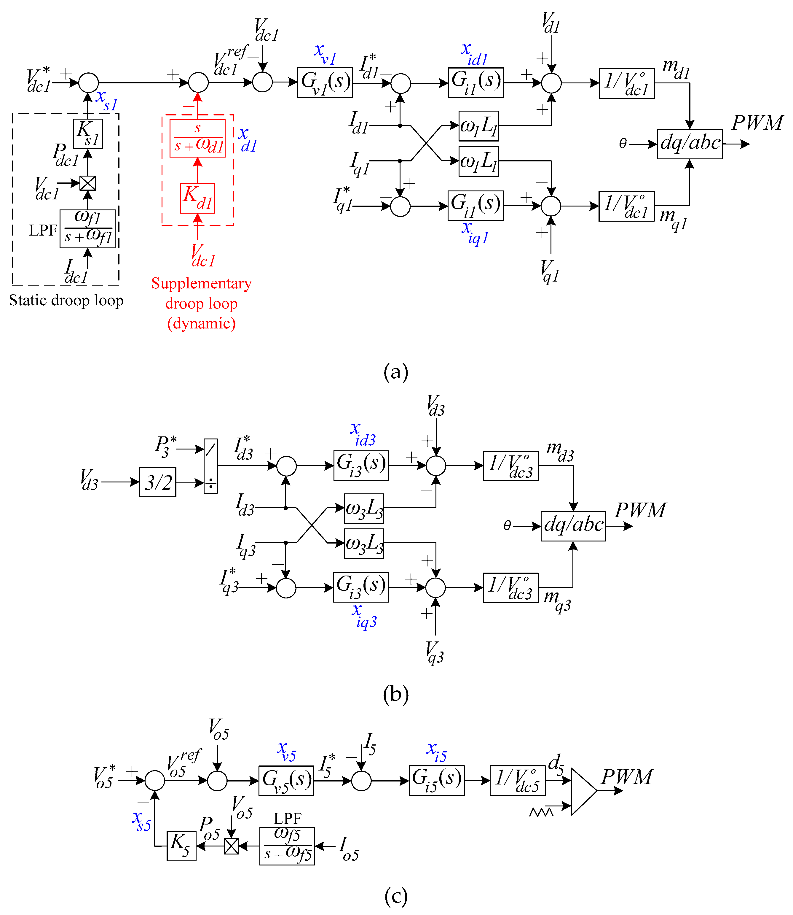
As shown in Figure 2a, the VSRs are equipped with an outer dc power sharing controller, an intermediate proportional-and-integral (PI) voltage controller () and an inner PI current control loop () [18]. The outer static droop loop processes the measured dc power via a low-pass filter (LPF) and through the static droop coefficient (). In Equations (1) and (2) and Figure 2a, the subscript “1” is replaced by “2” to represent the power circuit model and control loops of VSC2. The converter with the higher droop coefficient injects a less amount of dc power according to the equality [18].
2.2. Inversion Stations 3-4
The power circuit model of the inversion station is modeled in Equations (3) and (4).
The control structure of the inversion stations is shown in Figure 2b. PI inner current controllers () are implemented in the rotating - reference frame. The reference value of the -component of the controlled ac current is set to zero whereas the -component is defined by , assuming stiff ac grid conditions. In Equations (3) and (4) and Figure 2b, the subscript “3” is replaced by “4” to represent the power circuit model and control loops of VSC4.
2.3. DC/DC Conversion Stations 5-6
The power circuit model of the buck converter 5 is modeled in Equations (5) and (6).
Referring to Figure 2c, the control structure of the dc/dc conversion stations is similar to the rectification units; i.e. an outer power sharing loop, an intermediate PI dc voltage controller (), and an inner PI dc current controller () [18]. In Equations (5)–(7) and Figure 2c, the subscript “5” is replaced by “6” to represent the power circuit model and control loops of the buck converter 6.
2.4. MTDC Network
As shown in Figure 1, the infrastructure of the dc pool is represented by dc cables and is modeled in (8).
3. The Proposed Supplementary Dynamic Droop Loop
The proposed supplementary dynamic droop loop is shown in Figure 2a. The dc-link voltage () is applied to a gain () and a high-pass filter (HPF) with a cut-off frequency of to generate a compensation signal. It is shown in the following sections that the proposed supplementary droop loop contributes to the stabilization of the MTDC network. Note that the output compensation signal of the proposed loop is zero in the steady-state conditions and so no influence on the steady-state operation is yielded. In other words, the steady-state operation is solely dictated by the static droop gain () whereas the dynamic performance is independently enhanced by the supplementary dynamic droop loop. The proposed dynamic droop loops are implemented in VSC1 and VSC2.
4. Small-Signal Modeling and Stability Analysis of the MTDC System
In order to address the interaction dynamics issues among the MTDC entities and investigate the overall system stability, a linearized state-space model of the entire MTDC system is developed. The modeling procedures are detailed in Appendix A.
Throughout this paper, a non-linear time-domain simulation model for the entire MTDC system in Figure 1 is built under the Matlab/Simulink® environment (MathWorks, Natick, MA, USA) to verify the results. The power electronic converters are considered in the simulation model with the circuit structure and the control topology as shown in Figure 2. The complete model entities are built using SimPowerSystem® toolbox (MathWorks, Natick, MA, USA). The VSCs are simulated using average-model whereas the dc/dc converters are simulated using the switching-model. The simulation type is discrete with a sample time of 20 µs. The control and physical parameters of the MTDC system are given in Appendix B.
As a base case scenario, the two dc/dc converters supply a 0.3 p.u. dc resistive load whereas the power commands for both VSC3 and VSC4 is 1.4 and 0.5 p.u., respectively. The total supplied power from VSC1 and VSC2 is 0.8 and 1.4 p.u., respectively. The complete eigenvalues are shown in Table 1. The system is stable with left-hand sided eigenvalues on the -plane. It is shown from Table 1, and based on the participation factor analysis, that the states of the ac-dc filters (i.e. inductors or capacitors) in the VSCs and the dc/dc converters are associated with the highest damped modes. The current controllers of all converters reflect relatively high damped modes (–, –). Therefore, these modes are not detrimental to the system stability.
The most critical modes, i.e., –, are influenced by the dc voltage control loop of the VSRs. The power sharing controllers of the VSRs and dc/dc converters influence the relatively medium damped modes, i.e., , , and . Moreover, the MTDC cable parameters are correlated to the relatively high damped modes (, and ). The following subsections emphasize on the influence of these parameters on the system dynamics.
4.1. Influence of the MTDC Cables
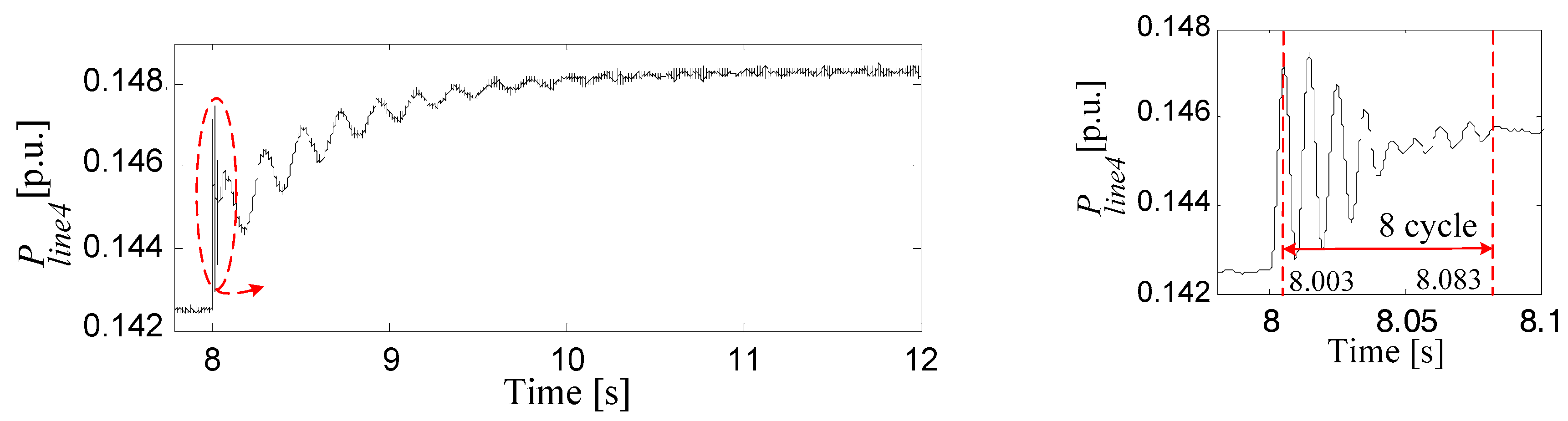
Table 2 shows the influence of reduced cables resistance () under a fixed inductance and a fixed cable length. It is clear that the reduced resistive negatively affects the system damping. The analytical results in Table 2 are verified using the time-domain simulations. As shown in Figure 3, the resistive component of the MTDC cables is reduced from to at = 8 s. The response has two oscillatory components: A fast response (magnified) corresponding to the modes associated with the MTDC cable and a much slower response associated with the static droop loop as will be shown hereunder. The magnified response in Figure 3 shows that a 0.08 s is needed to complete 8 cycles, and hence the frequency of oscillation is 100 Hz. Further, the envelope of the time-domain oscillating signal should decay to 0.37 p.u. of the initial amplitude in 0.06 s, whereas the damping ratio is 0.04. At the bottom of Table 2, the corresponding analytical results are 100 Hz, 0.06 s, and a damping ratio of 0.03. The analytical and time-domain results show a reasonable agreement, which validates the developed small-signal model of the MTDC system.
4.2. Influence of the Outer Power Sharing Loop and DC Voltage Controller of the VSRs
As shown in Table 1, the pairs () are the lowest damped modes with a frequency of oscillations of 7.5 Hz, a slow damping time of 0.59 s, and a damping ratio of 0.04. This pair is associated with the dc voltage control loop of both rectification stations. Referring to Figure 2a, the dc voltage controller of the VSRs processes the error signal , which is inherently in terms of and . Therefore, the dc voltage controller parameters and the static droop loop are responsible for defining the slowest dynamics of the MTDC system.
The influence of the dc-voltage controller of the VSRs is shown in Table 4. As shown, the increased proportional or integral gains positively affect the system stability. The damping ratio increases to 0.173 and 0.05 with 10 p.u. proportional and 4 p.u. integral gains, respectively. To verify these analytical results, the Simulink model is run under 10 p.u. proportional and 4 p.u. integral gains, and a step increase is applied in and from 1 to 1.05 p.u. at = 4s. The system response is shown in Figure 5 and the comparison between the time-domain simulations and the analytical results are depicted at the bottom of Table 4. The increased gains of the dc voltage controllers enhance the system damping, but with limited capabilities (Figure 5). Moreover, the controller gains might not be flexible enough to achieve the desired damping as they are designed according to the size of the dc-link capacitance. The controller design is also restricted to the bandwidth requirements to achieve a sufficient time-scale separation with respect to the outer power sharing and the inner current controllers.
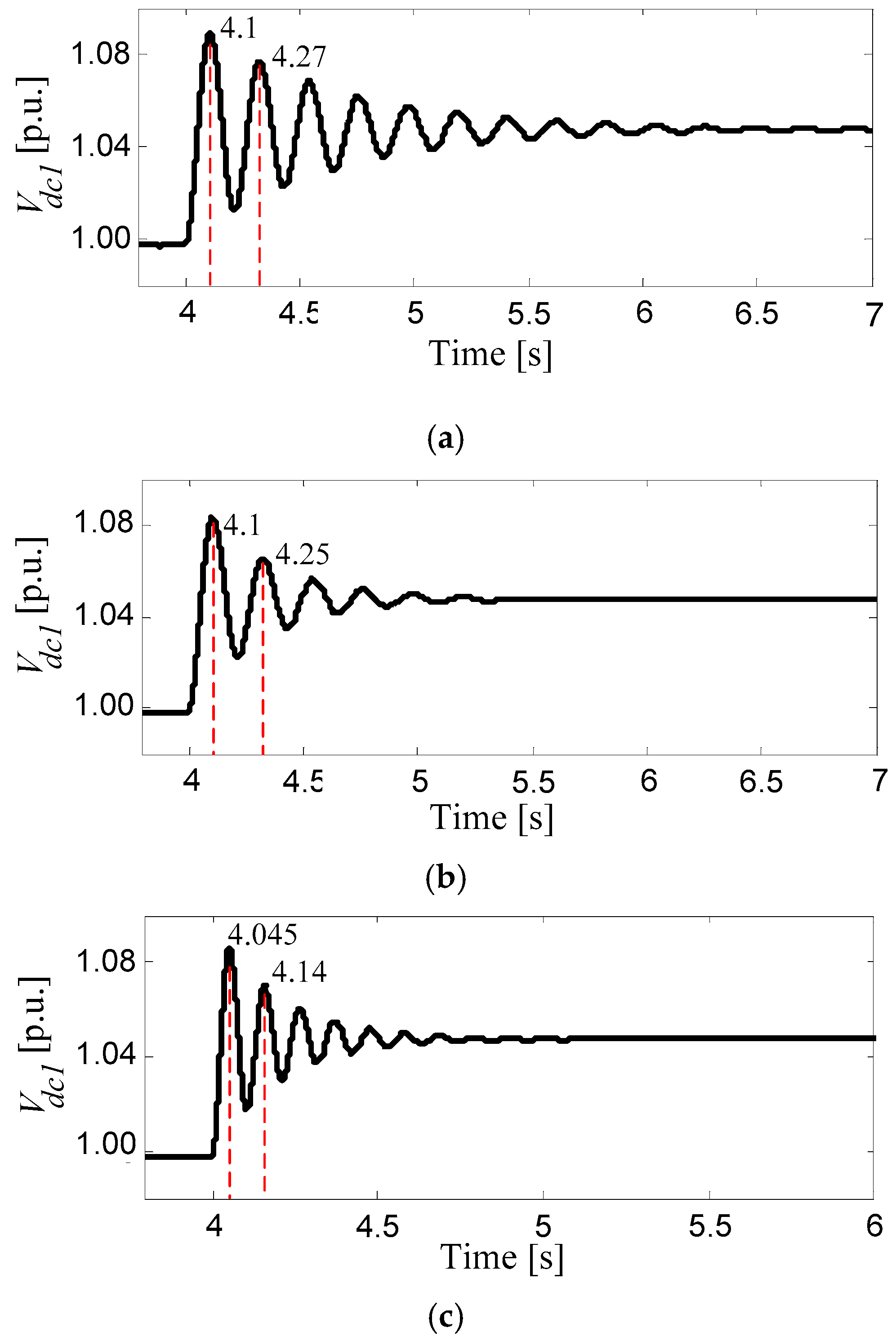
Table 5 details the positive effect of the increase of the static droop gains of both rectifiers on the most critical modes. The time-domain simulation results are shown in Figure 6 to validate the analytical results, where a step change in both the static droop coefficients of VSRs is applied from 1 to 5 p.u. at = 6 s and from 5 to 1 p.u. at = 8 s. At the bottom of Table 5, the analytical and modal analysis results reflect similar dynamics which confirms the accuracy of the developed models. Figure 6 shows that the more damped performance due to the higher droop gain is associated with a less regulated dc-link voltage, i.e., the value of the steady-state dc-link voltage decreases.
5. Influence of the Proposed Dynamic Droop Control Loop on the MTDC Stability
As the critical modes () are associated with the static droop gains of the power sharing loop of both rectifiers, the compensation signal is fed into this loop in order to dynamically enhance the stability margin.
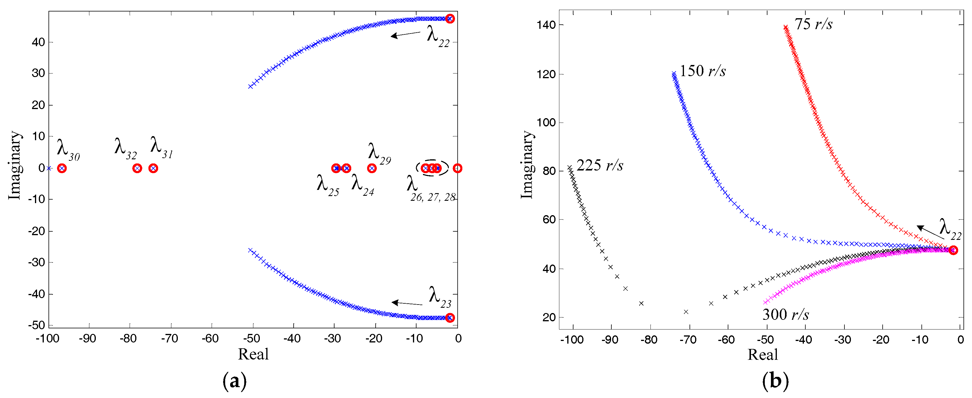
The small-signal state-space model is modified to include the dynamics of the proposed supplementary dynamic droop loop. The influence of the proposed supplementary loop is shown in Figure 7. The supplementary droop gains for both VSRs ( and ) are activated and increases from 0 to 10 with a cut-off frequency of the HPF of 300 rad/s. As shown in Figure 7a, the most critical modes () are relocated to more damped positions on the -plane. The damping ratio for these critical modes increases from 0.036 to 0.89 which implies the significant damping capabilities. Figure 7b shows the influence of the cut-off frequency of the HPF on the system damping. The operating frequency between 150 and 225 rad/s yields a better damping.
6. Evaluation Results
A non-linear time-domain simulation model for the entire MTDC system in Figure 1 is built under the Matlab/Simulink® environment. The complete model entities are built using SimPowerSystem® toolbox. The VSCs are simulated using average-model whereas the dc/dc converters are simulated using the switching-model. The simulation type is discrete with a sample time of 20µs. The control and physical parameters of the MTDC system are given in Appendix B.
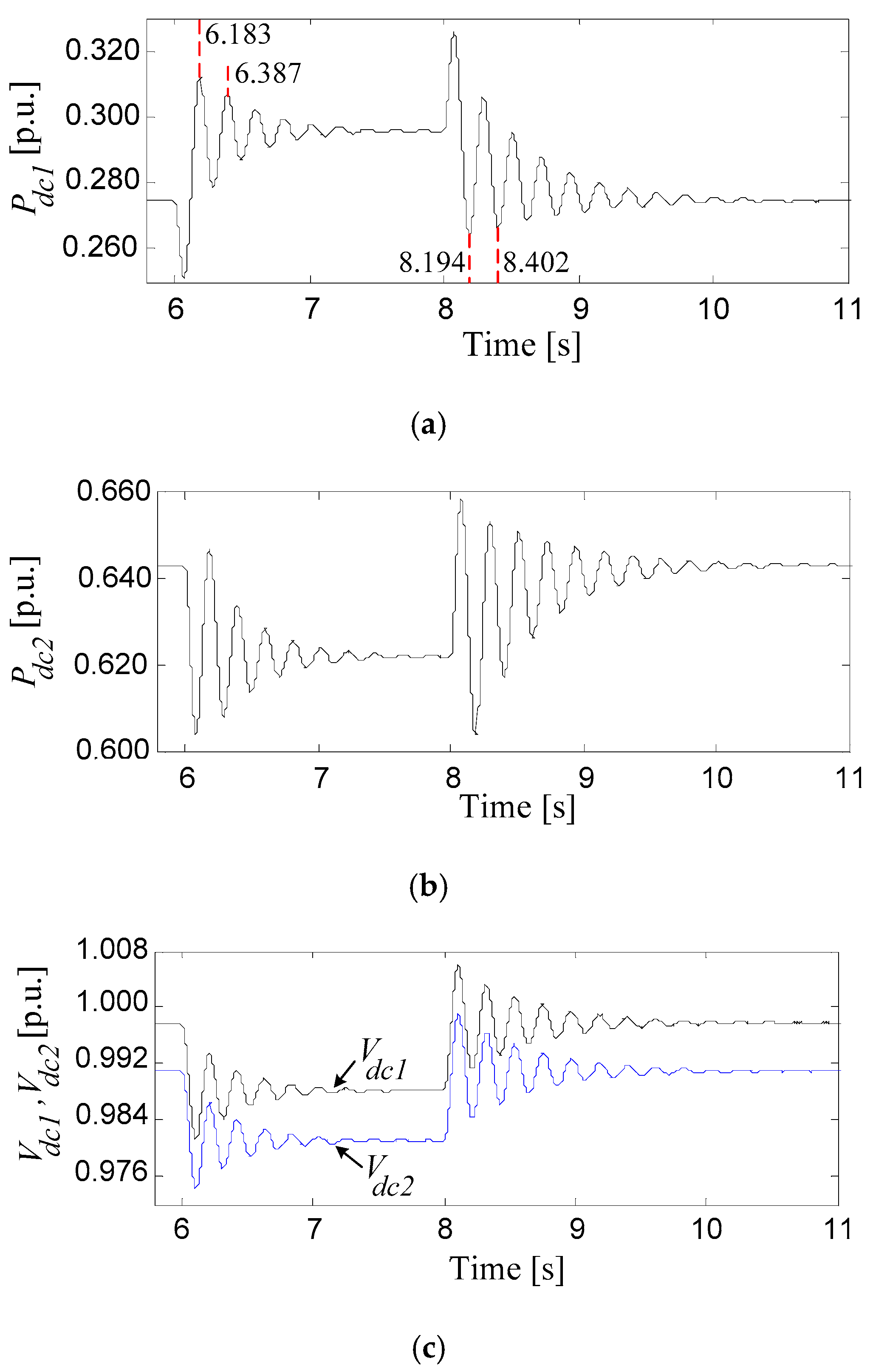
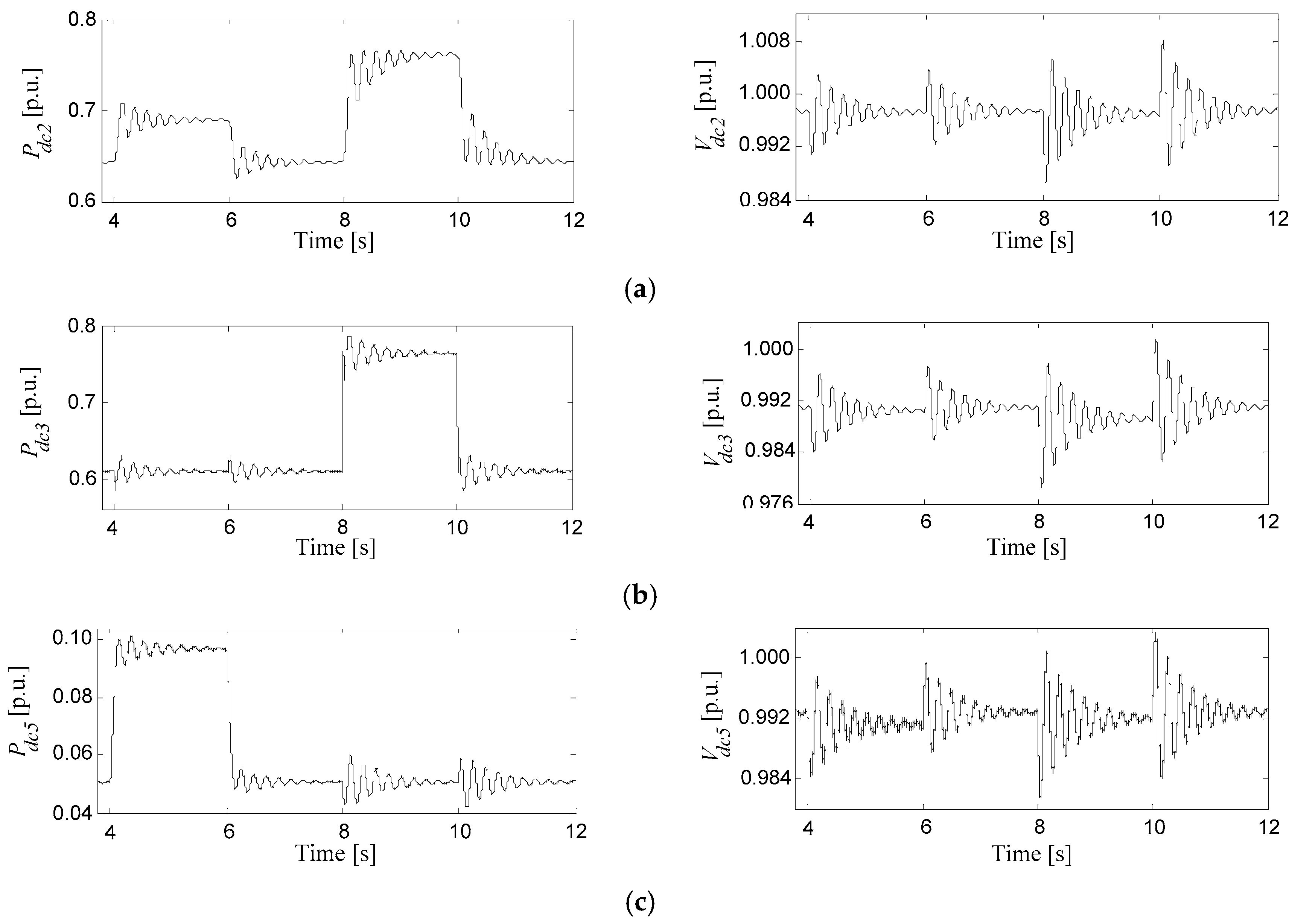
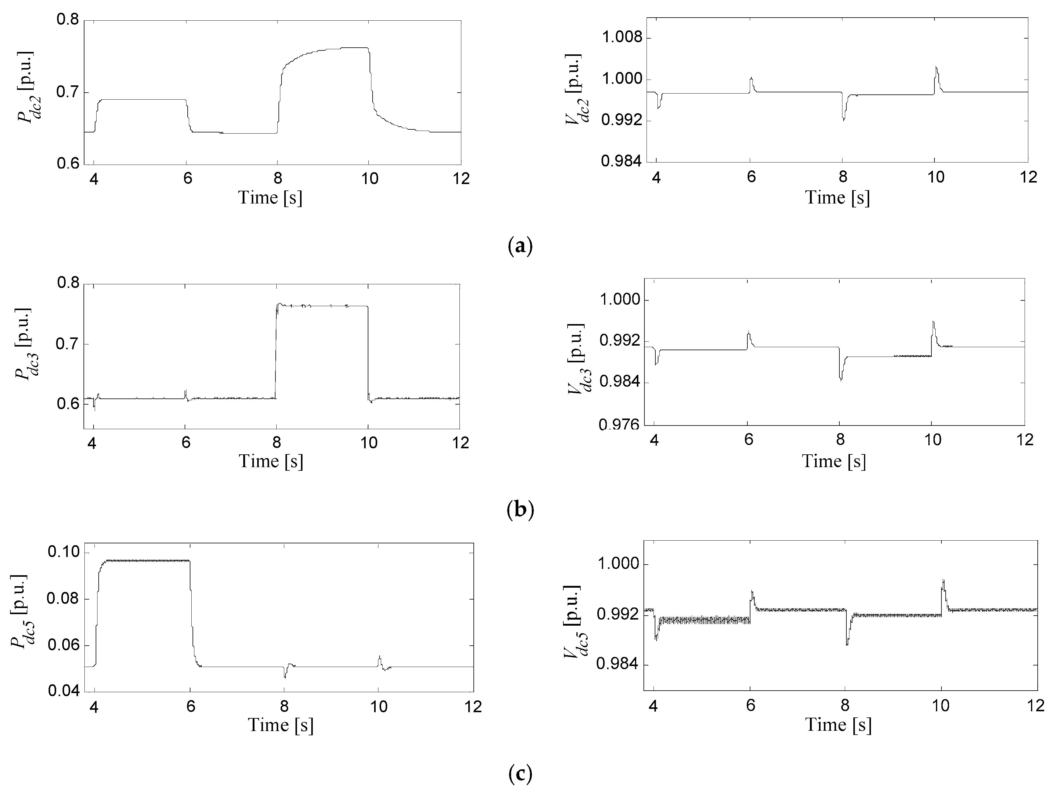
Table 6 depicts the loading sequence applied in the Simulink model to verify the effectiveness of the proposed supplementary droop compensator. Figure 8 shows the uncompensated system response at the terminals of VSCs 2,3 and dc/dc converter 5. The uncompensated system response suffers considerable oscillations associated with the lightly-damped modes of the static droop loop (). The enhanced droop loop is activated and the system response is shown in Figure 9. It is noted that the steady-state values of the injected powers and dc-link voltages are not changed. The proposed compensator decouples the predefined steady-state performance of MTDC entities and the damping of the system oscillations. It is also clear that the compensated system can operate under small static droop gains in order to maintain the highly regulated dc-link voltages throughout the dc pool and keeping the highly damped performance in the meanwhile.
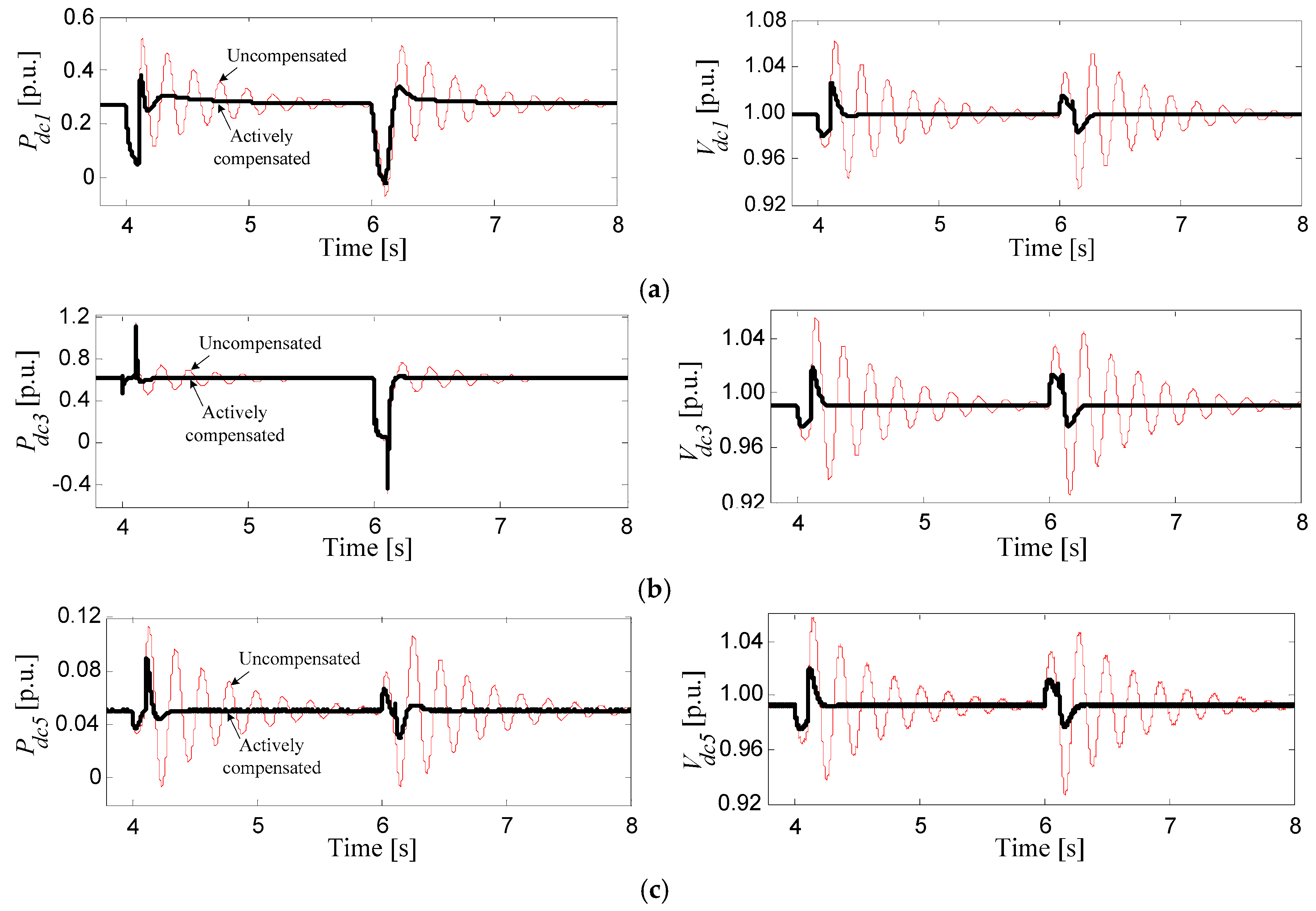
For further investigation, a five-cycle three-phase fault is applied at the ac-side of both VSC 1 and 3 at = 4 and 6 s, respectively. Figure 10a shows the dc power and terminal dc voltage of the VSC 1. The uncompensated response is still dominated by the slow-lightly-damped dynamics associated with the static droop loop. On the same figure, the actively compensated system shows a well-damped response. Figure 10b shows a similar response for VSC3. It is shown in Figure 10c that the healthy MTDC entities are affected by the faulty conditions. However, the proposed dynamic droop loop conveys the highly damped response throughout the dc pool.
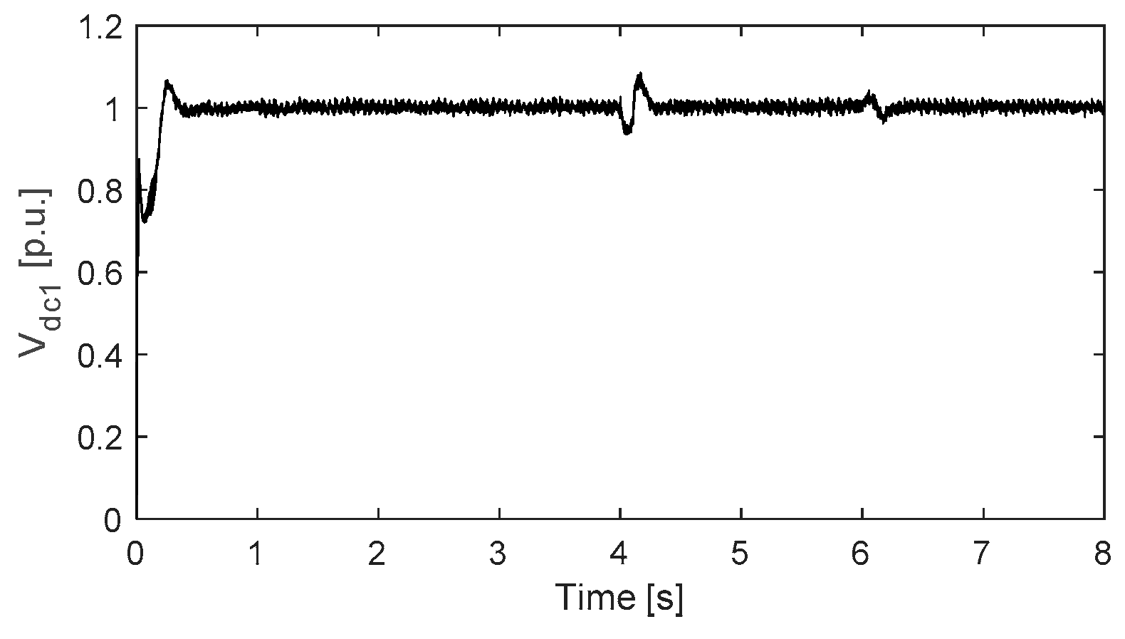
For further investigations, the average-based models of the VSCs in the preceding Matlab/Simulink time-domain simulations have been replaced by the switching-based Insulated-Gate-Bipolar-Junction-Transistor (IGBT) bridge and the 2-level PWM generator. The switching frequency is 1620 Hz. The compensated response in Figure 10a is reproduced under the switching-based VSCs, and the corresponding results are shown in Figure 11. Clearly, the results are very close which implies that the average-based time-domain simulation model is accurate.
7. Conclusions
This paper has presented the small-signal modeling and analysis of a six-terminal dc grid. The modeling approach depends on the development of the small-signal state-space sub-models of each entity in the MTDC network. A modal analysis is conducted to investigate the system stability under different operating conditions. It is found that the most critical eigenvalues are highly influenced by the static droop loop of both rectification stations. The damping of these modes can be improved by increasing the static droop gains. However, the variation of static droop gains should be subjected to the steady-state operational performance. Therefore, a second degree-of-freedom is added to the control structure of both VSRs by proposing a supplementary droop loop in order to enhance the system dynamics while preserving the steady-state performance (decoupling). The modal analysis shows the effectiveness of the proposed supplementary loop on the system damping. Throughout the analytical study, time domain simulation results are presented and compared to the modal analysis results: Both results show a close agreement which implies an accurate small-signal modeling. The proposed compensator is simple, designed using linear analysis tools and can be easily implemented on practical systems.
Funding
This research received no external funding.
Conflicts of Interest
The authors declare no conflict of interest.
Nomenclature
| Superscript “*” | The reference value of the variable. |
| Superscript “o” | The steady-state operating point of the variable. |
| Δ | The small-signal perturbed value of the variable |
| The differential operator. | |
| The imaginary number. | |
| The resistance and inductance of the MTDC dc cables. | |
| The resistance, inductance and capacitance of the power converters filters. | |
| The resistance and inductance of the dc cables at the load side of dc/dc converters. | |
| The dc-link capacitor and dc voltage. | |
| The dc current flowing in the MTDC dc network. | |
| The dc power and current at each conversion station. | |
| ,, | The terminal, input ac voltages, and ac current of the VSC. |
| The terminal and output voltage of the dc/dc converters. | |
| The filter and output current of the dc/dc converters. | |
| The common dc voltage at the load-side of the dc/dc converter. | |
| The proportional and integral gains of the proportional and integral (PI) current controller . | |
| The proportional and integral gains of the PI dc voltage controller | |
| The static and proposed supplementary droop coefficients of the VSCs. | |
| The conventional droop gain of the dc/dc converters. | |
| The angular frequency of the ac side of the VSC. | |
| The operating frequency of the controller filters. | |
| The direct- (-) and quadrature (-) components of the ac quantity . | |
| The duty ratio of the VSCs and dc/dc converters. |
Appendix A—Development of the State-Space Model of the MTDC Network
State-Space Model of the VSR
- ,
- ,
- , .
such that the matrices with subscript “”, “”, and “” model the power-sharing and the dc voltage control loop, the current control loop, and the power circuit, respectively, and are given as following.
State-Space Model of the VSI
, , .
such that the matrices with subscript “” and “” model the current control loop and the power circuit, respectively, and are given as following.
State-Space Model of the Buck DC/DC Converter
, ,
such that the matrices with subscript “”, “”, and “” model the dc voltage control loop, the current control loop, and the power circuit, respectively, and are given as following.
State-Space Model of the DC Networks
State-Space Model of DC/DC Converter Loads
The common resistive load of the dc/dc converters is interconnected through the load-side dc network. The state-space model of the load-side dc network is as follows
where , .
Entire State-Space Model of the MTDC System
The final state-space model of the MTDC system is as following.
,
where , , represents the element in the row “” and column “”, the row “”, the column “” of a matrix and is a zero matrix with rows and columns.
Appendix B—System Parameters
VSR1 (and VSR2)
VSI3 (and VSI4)
DC/DC Converter 5 (and 6)
DC Networks
References
- ABB. ABB HiPak™—IGBT Module 5SNA 1200G450300; 5SYA 1401-03 04-2012 datasheet; ABB: Zürich, Switzerland, 2012; pp. 1–9. [Google Scholar]
- Aredes, M.; Dias, R.; de Aquino, A.F.d.; Portela, C.; Watanabe, E. Going the distance. IEEE Ind. Electron. Mag. 2011, 5, 36–48. [Google Scholar] [CrossRef]
- Flourentzou, N.; Agelidis, V.G.; Demetriades, G.D. VSC-based HVDC power transmission systems—An overview. IEEE Trans. Power Electron. 2009, 24, 592–602. [Google Scholar] [CrossRef]
- Pinto, R.T.; Bauer, P.; Rodrigues, S.F.; Wiggelinkhuizen, E.J.; Pierik, J.; Ferreira, B. A novel distributed direct-voltage control strategy for grid integration of offshore wind energy systems through MTDC network. IEEE Trans. Ind. Electron. 2013, 60, 2429–2441. [Google Scholar] [CrossRef]
- Reeve, J. Multiterminal HVDC power systems. IEEE Trans. Power Appar. Syst. 1980, PAS-99, 729–737. [Google Scholar] [CrossRef]
- Rouzbehi, K.; Miranian, A.; Candela, J.I.; Luna, A.; Rodriguez, P. A Generalized Voltage Droop Strategy for Control of Multiterminal DC Grids. IEEE Trans. Ind. Appl. 2015, 51, 607–618. [Google Scholar] [CrossRef] [Green Version]
- Wang, Z.; Li, K.; Ren, J.; Sun, L.; Zhao, J.; Liang, Y.; Lee, W.; Ding, Z.; Sun, Y. A Coordination Control Strategy of Voltage-Source-Converter-Based MTDC for Offshore Wind Farms. IEEE Trans. Ind. Appl. 2015, 51, 2743–2752. [Google Scholar] [CrossRef]
- Mazumder, S.K.; Tahir, M.; Achrarya, K. Master-slave current-sharing control of a parallel dc-dc converter system over an RF communication interface. IEEE Trans. Ind. Electron. 2008, 55, 59–66. [Google Scholar] [CrossRef]
- Anand, S.; Fernandes, B.G.; Guerrero, J.M. Distributed control to ensure proportional load sharing and improve voltage regulation in low voltage dc microgrids. IEEE Trans. Power Electron. 2013, 28, 1900–1913. [Google Scholar] [CrossRef]
- Araujo, E.P.; Bianchi, F.D.; Ferre, A.J.; Bellmunt, O.G. Methodology for droop control dynamic analysis of multiterminal VSC-HVDC grids for offshore wind farms. IEEE Trans. Power Deliv. 2011, 26, 2476–2485. [Google Scholar] [CrossRef]
- -Alvarez, A.E.; Bianchi, F.; Ferré, A.J.; Gross, G.; Bellmunt, O.G. Voltage control of multiterminal VSC-HVDC transmission systems for offshore wind power plants—Design and implementation in a scaled platform. IEEE Trans. Ind. Electron. 2013, 60, 2381–2391. [Google Scholar] [CrossRef]
- Haileselassie, T.M.; Uhlen, K. Impact of dc line voltage drops on power flow of MTDC using droop control. IEEE Trans. Power Syst. 2012, 27, 1441–1449. [Google Scholar] [CrossRef]
- Chaudhuri, N.R.; Majumder, R.; Chaudhuri, B. System frequency support through multi-terminal dc (MTDC) grids. IEEE Trans. Power Syst. 2013, 28, 347–356. [Google Scholar] [CrossRef]
- Haileselassie, T.M.; Uhlen, K. Primary frequency control of remote grids connected by multi-terminal HVDC. In Proceedings of the IEEE Power and Energy Society General Meeting, Minneapolis, MN, USA, 25–29 July 2010; pp. 1–6. [Google Scholar]
- Ghaudhuri, N.R.; Chaudhuri, B. Adaptive droop control for effective power sharing in multi-terminal dc (MTDC) grids. IEEE Trans. Power Syst. 2013, 28, 21–29. [Google Scholar] [CrossRef]
- Chaudhuri, N.R.; Majumder, R.; Chaudhuri, B.; Pan, J. Stability analysis of VSC MTDC grids connected to multimachine ac systems. IEEE Trans. Power Deliv. 2011, 26, 2774–2784. [Google Scholar] [CrossRef]
- Liu, W.; Ooi, B.-T. Premium quality power park based on multi-terminal HVDC. IEEE Trans. Power Deliv. 2005, 20, 978–983. [Google Scholar] [CrossRef]
- Guerrero, J.M.; Vasquez, J.C.; Matas, J.; de Vicuña, L.G.; Castilla, M. Hierarchical control of droop-controlled ac and dc microgrids—A general approach toward standardization. IEEE Trans. Ind. Electron. 2011, 58, 158–172. [Google Scholar] [CrossRef]
Figure 1.
The MTDC system under study.

Figure 2.
The control structure of the MTDC entities. (a) VSRs (VSC1-2); (b) VSIs (VSC3-4); (c) DC/DC converters (5-6).
Figure 2.
The control structure of the MTDC entities. (a) VSRs (VSC1-2); (b) VSIs (VSC3-4); (c) DC/DC converters (5-6).

Figure 3.
Time domain simulation of the dc power flowing through line 4 following a step response from 0.04 to 0.005 at = 8 s.
Figure 3.
Time domain simulation of the dc power flowing through line 4 following a step response from 0.04 to 0.005 at = 8 s.

Figure 4.
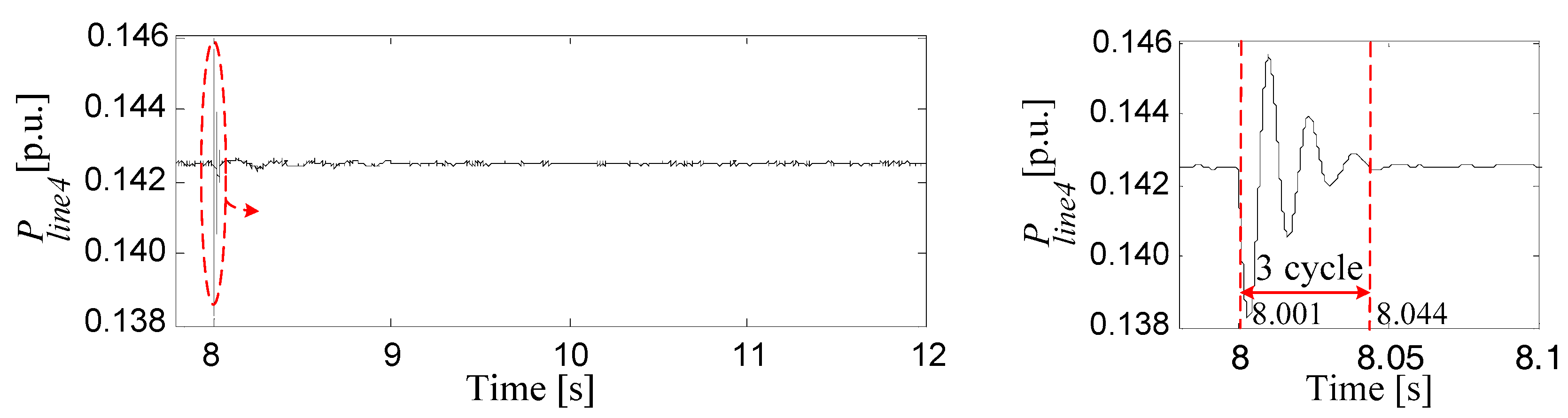
Time domain simulation of the dc power flowing through line 4 following the doubling of the MTDC lines inductance at = 8 s.
Figure 4.
Time domain simulation of the dc power flowing through line 4 following the doubling of the MTDC lines inductance at = 8 s.

Figure 5.
The dc-link voltage response of the VSC2 following a step variation in and from 1 to 1.05 p.u. at = 4s. (a) p.u. (b) p.u. (c) p.u.
Figure 5.
The dc-link voltage response of the VSC2 following a step variation in and from 1 to 1.05 p.u. at = 4s. (a) p.u. (b) p.u. (c) p.u.

Figure 6.
System response to a step change in the static droop gains for both VSRs from 1 to 5 and 5 to 1 p.u. at = 6 and 8 s, respectively. (a) Injected dc power from VSC1; (b) Injected dc power from VSC2; (c) DC-link voltages at VSCs 1 and 2.
Figure 6.
System response to a step change in the static droop gains for both VSRs from 1 to 5 and 5 to 1 p.u. at = 6 and 8 s, respectively. (a) Injected dc power from VSC1; (b) Injected dc power from VSC2; (c) DC-link voltages at VSCs 1 and 2.

Figure 7.
The effect of the proposed supplementary droop loop on the MTDC system stability—the proposed droop loop gain in both VSRs increases from zero to 10 (direction of arrow). (a) Cut-off frequency of the HPF = 300 rad/s; (b) Different cut-off frequencies of the HPF.
Figure 7.
The effect of the proposed supplementary droop loop on the MTDC system stability—the proposed droop loop gain in both VSRs increases from zero to 10 (direction of arrow). (a) Cut-off frequency of the HPF = 300 rad/s; (b) Different cut-off frequencies of the HPF.

Figure 8.
The uncompensated system response at different load-side disturbances according to Table 6; (a) VSC 2; (b) VSC 3; (c) DC/DC converter 5.
Figure 8.
The uncompensated system response at different load-side disturbances according to Table 6; (a) VSC 2; (b) VSC 3; (c) DC/DC converter 5.

Figure 9.
The influence of the proposed dynamic droop loop with the same load-side disturbances according to Table 6—; (a) VSC 2; (b) VSC 3; (c) DC/DC converter 5.
Figure 9.
The influence of the proposed dynamic droop loop with the same load-side disturbances according to Table 6—; (a) VSC 2; (b) VSC 3; (c) DC/DC converter 5.

Figure 10.
The compensated and uncompensated system response toward a five-cycle three-phase fault at ac-side of VSCs 1 and 3 at = 4 and 6 s, respectively. (a) VSC 1; (b) VSC 3; (c) DC/DC converter 5.
Figure 10.
The compensated and uncompensated system response toward a five-cycle three-phase fault at ac-side of VSCs 1 and 3 at = 4 and 6 s, respectively. (a) VSC 1; (b) VSC 3; (c) DC/DC converter 5.

Figure 11.
The compensated system response for Vdc1 under the switching-based models of all VSCs in Figure 1.
Figure 11.
The compensated system response for Vdc1 under the switching-based models of all VSCs in Figure 1.


Table 1.
Eigenvalues and Participation Factor Analysis of the MTDC System.
| Eigenvalue | Influencing State(s) | Contribution (p.u.) | |
|---|---|---|---|
| −562750 | 0.5, 0.5 | ||
| −124.6 ± j2353 | 0.48, 0.25, 0.25 | ||
| −126.5 ± j1138 | 0.29, 0.25, 0.18 | ||
| −123.7 ± j879 | 0.17, 0.16, 0.15 | ||
| −124.1 ± j620 | 0.24, 0.19, 0.14 | ||
| −124.1 ± j486 | 0.18, 0.14, 0.13 | ||
| −339.7± j1261.2 | 0.24, 0.24, 0.2 | ||
| −2027.6 | 0.39, 0.39 | ||
| −1797.1 | 0.35, 0.35 | ||
| −2500 | 0.73, 0.22 | ||
| −2500 | 0.73, 0.22 | ||
| −732.7 | 0.32, 0.32 | ||
| −250 | 0.24, 0.24 | ||
| −1.7 ± j47.4 | 0.25, 0.24 0.08 | ||
| −27.1 | 0.64, 0.24 | ||
| −29.5 | 0.72, 0.26 | ||
| −4.96 | 0.44, 0.44 | ||
| −6.1 | 0.46, 0.46 | ||
| −7.7 | 0.48, 0.48 | ||
| −20.8 | 0.49, 0.49 | ||
| −96.7 | 0.41, 0.41 | ||
| −74.3 | 0.38, 0.38 | ||
| −78.3 | 0.46, 0.45 | ||
| −2500 | 0.52, 0.42 | ||
| −100 | 0.28, 0.25 | ||
| −100 | 0.22, 0.2 | ||
| −100 | 0.32, 0.3 | ||
| −2500 | 0.85, 0.05 | ||
| −2500 | 0.45, 0.29 | ||
| −2500 | 0.49, 0.2 | ||
| −2500 | 0.75, 0.07 | ||
| −2500 | 0.71, 0.16 | ||
| −100 | 0.24, 0.19 | ||
| −100 | 0.34, 0.27 | ||
| −100 | 0.34, 0.3 | ||
| −100 | 0.68, 0.18 | ||
Table 2.
Influence of the DC Resistance of MTDC Cables.
| −124.6 ± j2353 | −62.1 ± j2355 | −30.8 ± j2356 | −15.2 ± j2356 | |
| −126.5 ± j1138 | −64.1 ± j1143 | −33 ± j1144 | −17.4 ± j1144 | |
| −123.7 ± j879 | −61.4 ± j886 | −30.3 ± j887.3 | −14.7 ± j887.7 | |
| −124.1 ± j620 | −62.1 ± j629.1 | −31.1 ± j631.4 | −15.5 ± j632 | |
| −124.1 ± j486 | −62 ± j498 | −30.9 ± j501 | −15.4 ± j502 | |
| −250 | −125 | −62.5 | −31.25 |
Modal Analysis vs. Time Domain Simulations
| Modal Analysis | Time Domain Simulations | ||
|---|---|---|---|
| 100 Hz—0.06 s—0.03 | Figure 3 | 100 Hz—0.045 s—0.04 | |
Table 3.
Influence of the Inductance of MTDC Cables.
| 1× length | 2× length | 3× length | 4× length | |
|---|---|---|---|---|
| −124.6 ± j2353 | −62.1 ± j1664.7 | −41.3 ± j1360 | −31 ± j1177 | |
| −126.5 ± j1138 | −64 ± j807.8 | −43.3 ± j661 | −34 ± j1261 | |
| −123.7 ± j879 | −61.2 ± j625.7 | −40.3 ± j513 | −33 ± j574 | |
| −124.1 ± j620 | −61.7 ± j444.2 | −41 ± j365 | −30 ± j445 | |
| −124.1 ± j486 | −61.5 ± j350.5 | −40.6 ± j289 | −30.6 ± j318 | |
| −250 | −125 | −83.3 | −62.5 |
Modal Analysis vs. Time Domain Simulations
| Modal Analysis | Time Domain Simulations | ||
|---|---|---|---|
| 70 Hz—0.016 s—0.138 | Figure 4 | 70 Hz—0.017 s—0.133 | |
Table 4.
Influence of the Proportional and Integral Gains.
of the DC Voltage Controller of the VSRs on the System Stability ()
| 1 p.u. | 5 p.u. | 10 p.u. | |
| −1.7 ± j47.4 | −3.56 ± j47.2 | −5.9 ± j46.9 | |
| 1 p.u. | 2 p.u. | 4 p.u. | |
| −1.7 ± j47.4 | −2.6 ± j66.8 | −4.6 ± j93.7 |
Table 5.
Influence of the Static Droop Gains of Both VSRs.
| 1 p.u. | 5 p.u. | 10 p.u. | 15 p.u. | |
|---|---|---|---|---|
| −1.7 ± j47.4 | −2.7 ± j48.9 | −3.9 ± j51 | −5.1 ± j53 |
Table 6.
Loading Sequence in the MTDC Network.
| VSC 3 | |||
|---|---|---|---|
| time = 4 s | time = 6 s | time = 8 s | time = 10 s |
| 0.1 → 0.2 p.u. | 0.2 → 0.1 p.u. | 0.6 → 0.75 p.u. | 0.75 → 0.6 p.u. |
© 2019 by the author. Licensee MDPI, Basel, Switzerland. This article is an open access article distributed under the terms and conditions of the Creative Commons Attribution (CC BY) license (http://creativecommons.org/licenses/by/4.0/).
Share and Cite
MDPI and ACS Style
Radwan, A.A.A. Small-Signal Stability Analysis of Multi-Terminal DC Grids. Electronics 2019, 8, 130. https://doi.org/10.3390/electronics8020130
AMA Style
Radwan AAA. Small-Signal Stability Analysis of Multi-Terminal DC Grids. Electronics. 2019; 8(2):130. https://doi.org/10.3390/electronics8020130
Chicago/Turabian StyleRadwan, Amr Ahmed A. 2019. "Small-Signal Stability Analysis of Multi-Terminal DC Grids" Electronics 8, no. 2: 130. https://doi.org/10.3390/electronics8020130
Note that from the first issue of 2016, this journal uses article numbers instead of page numbers. See further details here.