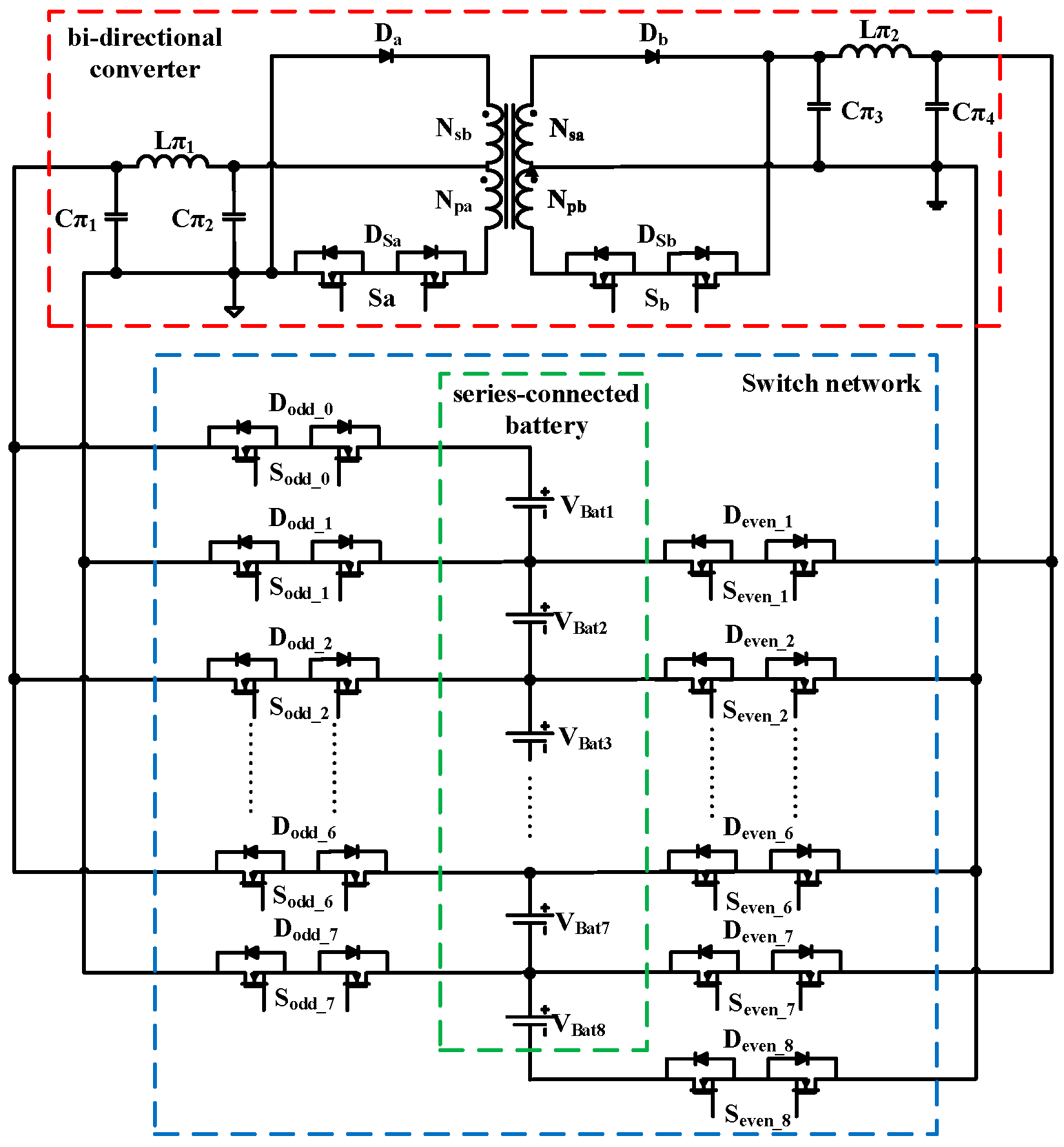
Article

A Fast Charging Balancing Circuit for LiFePO4 Battery

Department of Electrical Engineering, National Formosa University, No.64, Wunhua Rd., Huwei Township, Yunlin County 632, Taiwan
*
Author to whom correspondence should be addressed.
Electronics 2019, 8(10), 1144; https://doi.org/10.3390/electronics8101144
Submission received: 5 September 2019 / Revised: 27 September 2019 / Accepted: 2 October 2019 / Published: 10 October 2019
(This article belongs to the Special Issue Power Converters in Power Electronics)

Abstract

:
In this paper, a fast charging balancing circuit for LiFePO4 battery is proposed to address the voltage imbalanced problem of a lithium battery string. During the lithium battery string charging process, the occurrence of voltage imbalance will activate the fast balancing mechanism. The proposed balancing circuit is composed of a bi-directional converter and the switch network. The purpose of bi-directional is that the energy can be delivered to the lowest voltage cell for charging mode. On the other hand, the energy stored in the magnetizing inductors of the transformer can be charged back to the higher voltage cell in recycling mode. This novel scheme includes the following features: (1) The odd-numbered and even-numbered cells in the string with the maximum differential voltage will be chosen for balancing process directly. In this topology, there is no need to store and deliver the energy through any intermediate or the extra storing components. That is, the energy loss can be saved to improve the efficiency, and the fast balancing technique can be achieved. (2) There is only one converter to complete the energy transfer for voltage balancing process. The concept makes the circuit structure much simpler. (3) The structure has bi-directional power flow and good electrical isolation features. (4) A single chip controller is applied to measure the voltage of each cell to achieve the fast balancing process effectively. At the end of the paper, the practical test of the proposed balancing method on LiFePO4 battery pack (28.8 V/2.5 Ah) is verified and implemented by the experimental results.

1. Introduction

In recent years, lithium batteries and related techniques have developed and are widely used. The battery industries have experiences and capabilities for mass production of battery packs and modules. Battery packs and modules are composed of several battery cells for high power energy storing applications. However, there is a critical issue about imbalance of electric charge [1,2,3,4,5] within high power battery strings. The issue is caused by the characteristic [6], depth of discharge [7], and aging problem of each cell [8,9]. Based on the reasons above, when the battery string is being charged or discharged, the imbalance of each cell of the battery string becomes more serious. In addition, as the cycle of charging-discharging from the battery string increases, the internal resistance and the capacity of each cell will be varied to shorten the life cycle of battery strings.
In order to increase the efficiency and extend the lifetime of battery strings, a battery management system (BMS) [10,11,12,13,14,15,16] is a key feature which is utilized to monitor the parameters of the battery. Also, BMS plays an important role for management and protection of the battery. The main functions of BMS are monitoring, protection, and balancing parts [17,18]. The monitoring is to sense the relative key parameters from the battery packs, like voltage, current, and temperature. The protection is to avoid the situation of over-charging or over-discharging from the battery packs. The last one is about the balancing technique for each cell. In general, the balancing circuits can be divided into passive or active balancing topologies. The most common passive balancing schemes [19,20,21,22] utilize series resistors, series diodes, or Zener diodes to be the voltage dividers which are parallel to each cell for balancing purpose. These passive concepts with simple control methods and smaller size of balancing circuits can achieve a voltage equalizer for each cell during the process; however, the power losses and thermal issues will be the key factors to influence the balancing performance, accuracy, and the lifetime of cells. On the other hand, the active balancing topologies [23,24,25,26,27] can deliver the energy from higher voltage cell to lower one by using the storing elements and switches networks. Some of the active balancing schemes adopted multi-windings of the main transformer to fulfill the balancing performance with better electrical isolation feature, but the number of cells is limited by the windings; therefore, the dimension of the transformer will be increased for purpose of more balanced cells. In facts, these active balancing methods help to increase the efficiency and the performance during the balancing process, but they spent more time for delivering the energy from the high voltage cell to the low voltage cell. The reason is that if the highest voltage cell begins to charge to the lowest voltage cell, the energy flow has to be delivered through the other cells one by one to the target cell. Thus, the balancing path has a big problem of time wasting. In this paper, the proposed concept is to shorten the balancing time and to make the balanced cell being charged precisely. To recall the active balancing concept mentioned above, the basic concept of active balancing is to deliver the energy from the higher voltage battery to the lower voltage battery to achieve the balancing function for each cell. Nowadays, BMS is a core of many electric applications powered by batteries.
Based on the descriptions aforementioned, the paper proposed a fast charging balancing circuit for LiFePO4 battery pack. In this study, a digital signal processor (DSP) is adopted to implement the algorithm and to be the main controller.

2. Proposed Structure and Operation Mode Analysis

2.1. The Proposed Balancing Circuit

As shown in Figure 1, the proposed balancing method utilizes a bi-directional converter [28,29] to balance the voltage of each cell in a battery string. This method helps to deliver the energy from higher-voltage battery to lower-voltage battery directly. In other words, there is no more energy loss during the delivering process, and this technique can also shorten the balancing time effectively. In this study, the forward converter has good isolation feature and simple structure for bi-directional function. The strategy is to balance the voltage between the odd-numbered battery and the even-numbered battery which exist maximum differential voltage in the battery string. The switch network shown in blue dotted block is formed by several couples of MOSFETs with back-to-back connection, and each connection also becomes a bi-directional switch set with two MOSFETs which is connected with the cell. Hence, this connection can provide a bi-directional path to deliver the energy. In addition, each of the bi-directional switches set can avoid the other currents flowing through the cell during the balancing process.

2.2. The Operation Mode Analysis

The operation mode can be divided by two different modes. The first one is to balance the voltage from odd-numbered battery to even one. The other mode is to balance the voltage from even-numbered battery to odd one. The operation principle of these two modes will be discusses in detail below. In the following analysis, each battery denoted from VBat1 to VBat8 can be represented as a battery cell in the green dotted block in Figure 1.

2.2.1. The Operation Mode of Balancing Process from the Odd-Numbered Battery to the Even-Numbered Battery

The following analysis is stated for balancing from VBat1 to VBat8. The theoretical waveforms are shown in Figure 2.

Mode I—Charging Mode (t0 < t < t1)

As shown in Figure 3, the bi-directional switch set Sa, Sodd_0, Sodd_1, Seven_7, and Seven_8 are all turned on. The others are all turned off. In this mode, the current from VBat1 will charge to Lma through π filter I. In the meantime, the energy from the primary winding Npa can be transferred to the secondary winding Nsa; thus, Db is turned on by the forward bias. The current iNsa begins to charge to VBat8 through π filter II. The red dotted current path shows the charging condition.

Mode II—Recycling Mode (t1 < t < t2)

As shown in Figure 4, the bi-directional switch set Sa turns off, but Sodd_0, Sodd_1, Seven_7, and Seven_8 are all still turned on. The rest of switch sets are turned off. In this interval, the energy stored in Lma, and the current iLma remains continuously. Thus, iLma (shown with green dotted current) will flow through the primary winding Npa to induce a current iNsb from Nsb. The induced current iNsb also flows through π filter I and charge back to VBat1. During this mode, the energy stored in the magnetizing inductor can be released and also recycled to the battery(VBat1) effectively. At the right side of the converter, the energy of VBat8 is provided by π filter II.

2.2.2. The Operation Mode of Balancing Process from the Even-Numbered Battery to the Odd-Numbered Battery

The following analysis is stated for balancing from VBat8 to VBat1, and Figure 5 shows the theoretical waveforms during the balancing process.

Mode III—Charging Mode (t2 < t < t3)

As shown in Figure 6, the bi-directional switch set Sb, Sodd_0, Sodd_1, Seven_7, and Seven_8 are all turned on. The others are all turned off. The current from VBat8 will charge to Lmb through π filter II and also deliver the energy from the primary winding Npb to the secondary winding Nsb. In this transferring state, Da is turned on, and iNsb starts to charge to VBat1 through π filter I. The charging path is shown in red-dotted current.

Mode Ⅳ-Recycling Mode (t3 < t < t4)

As shown in Figure 7, the bi-directional switch set Sb turns off, but Sodd_0, Sodd_1, Seven_7, and Seven_8 are all still turned on. The rest of the switch sets are turned off. In this interval, the energy stored in Lmb, and the current iLmb remains continuously. Thus, iLmb (shown with green dotted current) will flow thru the primary winding Npb to induce a current iNsa from Nsa. The induced current iNsa also flows through π filter II and charge back to VBar8. During this mode, the energy stored in the magnetizing inductor can be released and also recycled to the battery (VBat8) effectively. At the left side of the converter, the energy of VBat1 is provided by π filter I. In this recycling mode, the energy is saved during this interval.

3. Design Consideration and Specification of Cell

In this part, the design consideration is discussed in detail. Table 1 lists the experiment key parameters (switching frequency, duty cycle, turns ratio, capacitance, and inductance) in this study. In addition, Table 2 is the specification of LiFePO4 battery. These parameters of battery help to design the charger and the related components. At first, the turns ratio (NS/NP) of the transformer has to be determined by using the nominal voltage of cell. In order to simplify the derivation, all the switches are assumed to be ideal. Besides, this application is operated in low voltage, the power switches and the diodes can be selected for low power rating to decrease the cost of the converter.
The turns ratio can be derived by the voltage of the charging behavior. Refer to Figure 8, Vin is fed in π filter I, and the voltage across the primary side NPa is also the Vin (assuming the filters and the switches are ideal). At the secondary side, the voltage VNsa across NSa is induced by NPa. During the charging state from Vin to Vo, the condition ( V NSa V o ) > V D has to be satisfactory to turn on the diode Db. Therefore, the charging path can be established as red dotted current.
Based on (1), the across voltage on the diode has to be higher than the cut-in bias VD for turning on the diode. That is, the input voltage Vin is definitely higher than Vo. After the battery balancing process ends, Vin will approach to the charging voltage of the battery and also to be identical to Vo In the steady state, Vin = Vo. Thus, the equation (1) can be rewritten which is shown in (2).
( V in × N s N p V o ) > V D
  V in × ( N s N p 1 ) > V D
After rearranged (2), the equation (3) can be obtained as below.
N s N p > V D V in + 1
In order to obtain the turns ratio from (3), the voltage of Vin is 3.3V, and the forward bias voltage of VD is 0.45 V respectively. Based on these parameters which are substituted into (4), the derived turns ratio is 1.14.
N s N p > [ 0.45 3.3 + 1 ] = 1.14
In this study, the actual turns ratio is chosen for 1.2 in this experiment.

4. Fast Battery Balancing Control Strategy and the Algorithm

The main digital controller utilized in this proposed structure is dsPIC33EP128GM304 from Microchip Technology. The first step of the procedure is to sense the voltage of each battery by the voltage detector circuit and to send the information to the processor with A/D converters. After analyzing from the processor, the battery cell in the string which needs to be activated for balancing will be chosen by the processor. In other words, the related switches (S1, S2, Sodd_0~Sodd_7, and Seven_1~Seven_8) around the imbalanced battery cells will be turned on or off for balancing process. Figure 9 shows the structure of the proposed fast battery charging balancing circuit.
When the battery string is being charged, the digital processor utilizes A/D converters and the voltage detection circuit to detect the battery voltage from VBat1 to VBat8. After detecting the actual battery voltage, the average voltage Vavg can be calculated by the processor, and the formula is shown in (5).
V avg = V bat 1 + V bat 2 + + V bat 8 8
Besides, the start-up voltage Vbalance_start for balancing process is shown in (6), and △V is the threshold voltage which can be determined by users’ demand.
V balance _ start = V avg + Δ V
If any of the battery voltage is higher than the preset of Vbalance_start, the proposed balancing mechanism will be activated. Once the battery balancing mechanism enables, these batteries which exist the maximum differential voltage between the odd-numbered and even-numbered will be selected. During the balancing procedure, the digital processor keeps detecting the batteries voltage and refreshing the average voltage. Until the highest battery voltage VH     Vavg or the lowest battery voltage VL     Vavg, the balancing process will be finished. Figure 10 is the flow chart of dynamic battery charging balancing strategy.
In the balancing process, the voltage of each cell will be kept detecting and measuring all the time. In order to sense the voltage of each cell precisely, and to avoid the load effect between the cell and the input of the analog to digital converter (ADC), the detection circuit for battery voltage is adopted. From Figure 9, the detection of battery voltage is composed of a differential-voltage operational amplifier (OPA) and a low pass filter (LPF) to achieve the voltage measurement of a cell. The function of LPF is to filter the high frequency noise at the output of OPA. Then, the output of LPF will connect to the ADC’s input of the MCU. In facts, the charging voltage of cell, VBat is 3.6 V, but the maximum input voltage of the ADC is 3 V; therefore, the proportion of the resistors around the OPA needs to be considered (R1 = R3, R2 = R4) for full scale voltage as shown in (7). In this circuit, the LPF has no attenuation in low frequency. Thus, V 1 =   V O . In the meanwhile, the voltage of cell can also be measured by the voltage recorder. The detection of battery voltage circuit is shown in Figure 11.
  V O = ( R 2 R 1 ) × V bat

5. Experimental and Simulation Results

In order to verify the proposed battery charging balancing circuit with the theoretical derivation, Figure 12, Figure 13, Figure 14, Figure 15 and Figure 16 show the triggering waveforms for building up the balancing loop and the related waveforms when VBat1 charges to VBat8. In the opposite, Figure 17, Figure 18, Figure 19, Figure 20 and Figure 21 provide the waveforms when VBat8 charges to VBat1. These waveforms are measured and simulated to prove that the balancing process is feasible and implemented.

5.1. Waveforms for VBat1 Charges to VBat8

In this section, the simulation results are shown to compare with the experiments. Figure 11 shows the gate signals for turning on Sodd_0, Sodd_1, Seven_7, and Seven_8.
When the balancing loop keeps turning on all the time, Sa also turns on (VGSa: high) in the meantime. The converter goes to charging mode when VBat1 charges to VBat8. If Sa turns off (VGSa: low), the converter goes to recycling mode. In recycling mode, the rest of energy stored in the magnetizing inductor from the previous stage will charge back to VBat1. The following experiments and simulations are shown from Figure 13, Figure 14, Figure 15 and Figure 16.
Referred to Figure 15 and Figure 16, when the converter is being operated in charging mode, iNpa starts to increases for charging the magnetizing inductor and to deliver the energy to lower voltage cell. Once the converter goes to recycling mode, iNsb is induced by the magnetizing inductor. Thus, the stored energy is charged back to the higher voltage cell through the filter. From these two figures below, the current direction of iNpa is opposite to iNsb. This phenomenon proves that the recycling mode is successful.

5.2. Waveforms for VBat8 Charges to VBat1

This operation principle is almost the same as the previous section, but the only difference is that the charging direction is inverse (VBat8 charges to VBat1). The simulation results are shown to compare with the experiments. Figure 17 shows the gate signal for turning on Sodd_0, Sodd_1, Seven_7, and Seven_8 for building up the charging path. In addition, Figure 18, Figure 19, Figure 20 and Figure 21 present the related waveforms when VBat8 charges to VBat1.
After the balancing loop established, Sb turns on in the meantime as well. The converter enters into charging mode when VBat8 charges to VBat1. However, if Sb turns off, the converter moves to recycling mode and the rest of energy stored in the magnetizing inductor will charge back to VBat8. The experiments and simulations are shown from Figure 18, Figure 19, Figure 20 and Figure 21.
To sum up the measurements and simulations above, these results are compared and proved that the proposed fast charging and balancing circuit is feasible.
Before the balancing process starts, each of the battery cells has been discharged for test and experiment. The open loop voltage of each cell is listed in Table 3 from VBat1 to VBat8 individually. When the cell is being charged with 1C current, the △V is set for 0.03 V during the balancing interval I to IV. If the voltage reaches to 3.5 V, the △V is set from 0.03 V to 0.02 V during the balancing interval V to VII. As the battery voltage rises from 3.5 V to 3.6 V at interval V, the main concept of choosing △V is set for lower voltage to make the balancing process much more precise. During the experiments, the voltage and the curve of each cell is measured and drawn by a voltage recorder (model number: midi LOGGER GL800, manufacture: GRAPHTEC).
From Figure 22, each of these cells has 7 balancing intervals from interval I to VII. The balancing time and the energy loss of the proposed converter from I to VII are summarized as Table 4. As shown in Table 4, the balancing time becomes shorter when each cell reaches to the charging voltage 3.6 V. Also, the energy loss of the converter gets lower because the balancing process goes to the end.
In Table 5, the measurements and experimental results are listed. The total balancing time is to sum up the time from interval I to VII. To compare with the conventional balancing method, the proposed concept can shorten the balancing time effectively. Besides, after the balancing process, the maximum differential voltage among the balanced cells is 0.018 V.
As mentioned above, △V is determined by user’s demand and the balancing performance. If the user requires a lower differential voltage among these cells in the battery string, △V has to be set lower to achieve the better balancing performance; however, it takes more time for the balancing process. Table 6 gives a comparison of different value of △V. In the opposite, a higher △V will obtain a worse balancing performance even the balancing time is shorter.

6. Conclusions

The paper proposes a fast charging balancing circuit for LiFePO4 battery. The main concept is to give a fast voltage balancing strategy for each cell within a single battery string. In this study, a novel bi-directional forward converter is utilized and connected with the balancing bi-directional switches network to form a bi-directional battery balancing circuit.
The feature of the proposed scheme is to balance the maximum differential voltage between the odd-numbered battery and the even-numbered battery in the battery string directly. In order to verify the proposed structure, a fast battery charging circuit for a string with 8 pieces of cell (3.6 V/2.5 Ah for each cell) is implemented. In addition, the merit of this circuit can also avoid over charging situation during the balancing process.
Referred to the experimental and simulation results in previous section, a faster charging balancing circuit for a battery string is achieved. The advantage of this scheme also improves the precision of each cell after balancing procedure. The future research will keep improving the balancing algorithms for random cells in the battery string. Moreover, the proposed study can save more time during the balancing process. At present, industrial applications, electric vehicles batteries, and higher capacity batteries are always composed of many cells connected in series and parallel; therefore, the characteristics and aging phenomenon of each cell have to be concerned with care. In the near future, a battery management system can be added for the proposed balancing circuit to obtain a high precision and faster battery equalizer for each cell.

Author Contributions

S.-T.W. and Y.-N.C. conceptualized and supervised the experiments of the research. S.-T.W. revised and modified the research data into paper format. Y.-N.C. provided the testing bench of the research. C.-Y.C. was in charge of software environment building up. Y.-T.C. was in charge of measurement, and data recording.

Funding

This research received no external funding.

Conflicts of Interest

The authors declare no conflict of interest.

References

  1. Huang, W.; Qahouq, J.A.A. Energy Sharing Control Scheme for State-of-Charge Balancing of Distributed Battery Energy Storage System. IEEE Trans. Ind. Electron. 2015, 62, 2764–2776. [Google Scholar] [CrossRef]
  2. Narayanaswamy, S.; Kauer, M.; Steinhorst, S.; Lukasiewycz, M.; Chakraborty, S. Modular Active Charge Balancing for Scalable Battery Packs. IEEE Trans. Very Large Scale Integr. Syst. 2017, 25, 974–987. [Google Scholar] [CrossRef]
  3. Chatzinikolaou, E.; Rogers, D.J. Performance Evaluation of Duty Cycle Balancing in Power Electronics Enhanced Battery Packs Compared to Conventional Energy Redistribution Balancing. IEEE Trans. Power Electron. 2018, 33, 9142–9153. [Google Scholar] [CrossRef] [Green Version]
  4. Baughman, A.C.; Ferdows, M. Double-Tiered Switched-Capacitor Battery Charge Equalization Technique. IEEE Trans. Ind. Electron. 2008, 55, 2277–2285. [Google Scholar] [CrossRef]
  5. Einhorn, M.; Roessler, W.; Fleig, J. Improved Performance of Serially Connected Li-Ion Batteries with Active Cell Balancing in Electric Vehicles. IEEE Trans. Veh. Technol. 2011, 60, 2448–2457. [Google Scholar] [CrossRef]
  6. Einhorn, M.; Conte, F.V.; Kral, C.; Fleig, J. Comparison, Selection, and Parameterization of Electrical Battery Models for Automotive Applications. IEEE Trans. Power Electron. 2013, 28, 1429–1437. [Google Scholar] [CrossRef]
  7. Duggal, I.; Venkatesh, B. Short-Term Scheduling of Thermal Generators and Battery Storage with Depth of Discharge-Based Cost Model. IEEE Trans. Power Syst. 2015, 30, 2110–2118. [Google Scholar] [CrossRef]
  8. Mejdoubi, A.E.; Chaoui, H.; Gualous, H.; Bossche, P.V.D.; Omar, N.; Mierlo, J.V. Lithium-Ion Batteries Health Prognosis Considering Aging Conditions. IEEE Trans. Power Electron. 2019, 34, 6834–6844. [Google Scholar] [CrossRef]
  9. Xiong, R.; Zhang, Y.; Wang, J.; He, H.; Peng, S.; Pecht, M. Lithium-Ion Battery Health Prognosis Based on a Real Battery Management System Used in Electric Vehicles. IEEE Trans. Veh. Technol. 2019, 68, 4110–4121. [Google Scholar] [CrossRef]
  10. Li, L.; Xu, Z.; Zhu, J.; Jing, X.; Shuntao, X. Research on dynamic equalization for lithium battery management system. In Proceedings of the 2017 29th Chinese Control and Decision Conference (CCDC), Chongqing, China, 28–30 May 2017. [Google Scholar]
  11. Steinhorst, S.; Lukasiewycz, M. Formal Approaches to Design of Active Cell Balancing Architectures in Battery Management Systems. In Proceedings of the 2016 IEEE/ACM International Conference on Computer-Aided Design (ICCAD), Austin, TX, USA, 7–10 November 2016. [Google Scholar]
  12. Garche, J.; Jossen, A. Battery Management Systems (BMS) for Increasing Battery Life Time. In Proceedings of the Third International Telecommunications Energy Special Conference, Dresden, Germany, 7–10 May 2000. [Google Scholar]
  13. Lawder, M.T.; Suthar, B.; Northrop, P.W.C.; De, S.; Hoff, C.M.; Leitermann, O.; Crow, M.L.; Santhanagopalan, S.; Subramanian, V.R. Battery Energy Storage System (BESS) and Battery Management System (BMS) for Grid-Scale Applications. Proc. IEEE 2014, 102, 1014–1030. [Google Scholar] [CrossRef]
  14. Wang, J.B.; Koa, D. Design and Implementation of a Battery Module. In Proceedings of the 2014 International Conference on Intelligent Green Building and Smart Grid (IGBSG), Taipei, Taiwan, 23–25 April 2014. [Google Scholar]
  15. Bonfiglio, C.; Roessler, W. A Cost Optimized Battery Management System with Active Cell Balancing for Lithium Ion Battery Stacks. In Proceedings of the IEEE Vehicle Power Propulsion Conference, Dearborn, MI, USA, 7–10 September 2009. [Google Scholar]
  16. Lan, C.W.; Lin, S.S.; Syue, S.Y.; Hsu, H.Y.; Huang, T.C.; Tan, K.H. Development of an Intelligent Lithium-Ion Battery-Charging Management System for Electric Vehicle. In Proceedings of the 2017 International Conference on Applied System Innovation (ICASI), Sapporo, Japan, 13–17 May 2017. [Google Scholar]
  17. Elsayed, A.T.; Lashway, C.R.; Mohammed, O.A. Advanced Battery Management and Diagnostic System for Smart Grid Infrastructure. IEEE Trans. Smart Grid 2016, 7, 897–905. [Google Scholar]
  18. Xu, D.; Wang, L.; Yang, J. Research on Li-ion Battery Management System. In Proceedings of the 2010 International Conference on Electrical and Control Engineering, Wuhan, China, 25–27 June 2010. [Google Scholar]
  19. Shibata, H.; Taniguchi, S.; Adachi, K.; Yamasaki, K.; Ariyoshi, G.; Kawata, K.; Nishijima, K.; Harada, K. Management of serially-connected battery system using multiple switches. In Proceedings of the 4th IEEE International Conference on Power Electronics and Drive Systems, Denpasar, Indonesia, 25–25 October 2001. [Google Scholar]
  20. Amin; Ismail, K.; Nugroho, A.; Kaleg, S. Passive balancing battery management system using MOSFET internal resistance as balancing resistor. In Proceedings of the 2017 International Conference on Sustainable Energy Engineering and Application, Jakarta, Indonesia, 23–24 October 2017. [Google Scholar]
  21. Harada, K.; Taniguchi, S.; Adachi, K.; Ariyoshi, G.; Kawata, Y. On the removing of a less quality battery from a series-connected system. In Proceedings of the INTELEC, Twenty-Second International Telecommunications Energy Conference, Phoenix, AZ, USA, 10–14 September 2000. [Google Scholar]
  22. Luo, W.; Lv, J.; Song, W.; Feng, Z. Study on passive balancing characteristics of serially connected lithium-ion battery string. In Proceedings of the 2017 13th IEEE International Conference on Electronic Measurement & Instruments, Yangzhou, China, 20–22 October 2017. [Google Scholar]
  23. Kutkut, N.H.; Wiegman, H.L.N.; Divan, D.M.; Novotny, D.W. Design considerations for charge equalization of an electric vehicle battery system. IEEE Trans. Ind. Appl. 1999, 35, 28–35. [Google Scholar] [CrossRef] [Green Version]
  24. Wei, X.; Zhu, B. The research of vehicle power Li-ion battery pack balancing method. In Proceedings of the 2009 9th International Conference on Electronic Measurement & Instruments, Beijing, China, 16–19 August 2009. [Google Scholar]
  25. Sooksood, K.; Stieglitz, T.; Ortmanns, M. An Active Approach for Charge Balancing in Functional Electrical Stimulation. IEEE Trans. Biomed. Circuits Syst. 2010, 4, 162–170. [Google Scholar] [CrossRef] [PubMed]
  26. Li, S.; Mi, C.C.; Zhang, M. A High-Efficiency Active Battery-Balancing Circuit Using Multiwinding Transformer. IEEE Trans. Ind. Appl. 2013, 49, 198–207. [Google Scholar] [CrossRef]
  27. Wei, X.; Zhao, X.; Dai, H. The application of flyback DC/DC converter in Li-ion batteries active balancing. In Proceedings of the 2009 IEEE Vehicle Power and Propulsion Conference, Dearborn, MI, USA, 7–10 September 2009. [Google Scholar]
  28. Hosseinzadeh, M.; Salmasi, F.R. Robust Optimal Power Management System for a Hybrid AC/DC Micro-Grid. IEEE Trans. Sustain. Energy 2015, 6, 675–687. [Google Scholar] [CrossRef]
  29. Schonbergerschonberger, J.; Duke, R.; Round, S.D. DC-Bus Signaling: A Distributed Control Strategy for a Hybrid Renewable Nanogrid. IEEE Trans. Ind. Electron. 2006, 53, 1453–1460. [Google Scholar] [CrossRef]
Figure 1. The proposed fast charging balancing circuit for LiFePO4 battery.
Electronics 08 01144 g001
Figure 2. The theoretical waveforms in balancing process from VBat1 to VBat8.
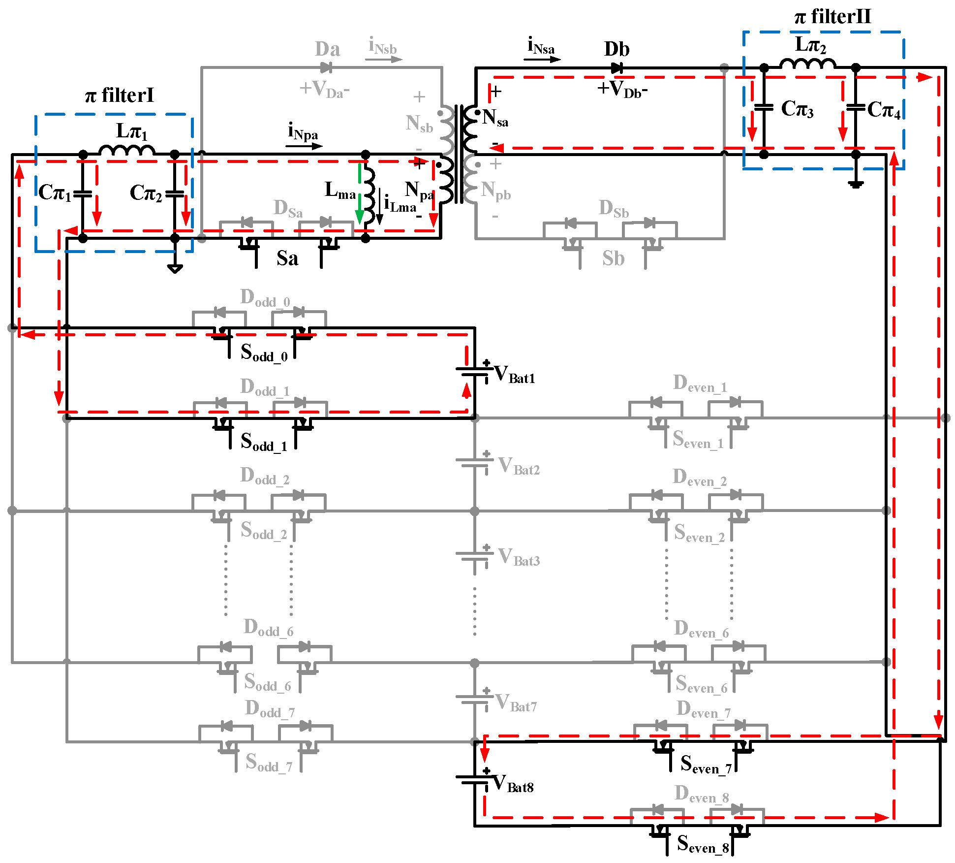
Electronics 08 01144 g002
Figure 3. Mode I, the battery balancing process from higher VBat1 to lower VBat8.
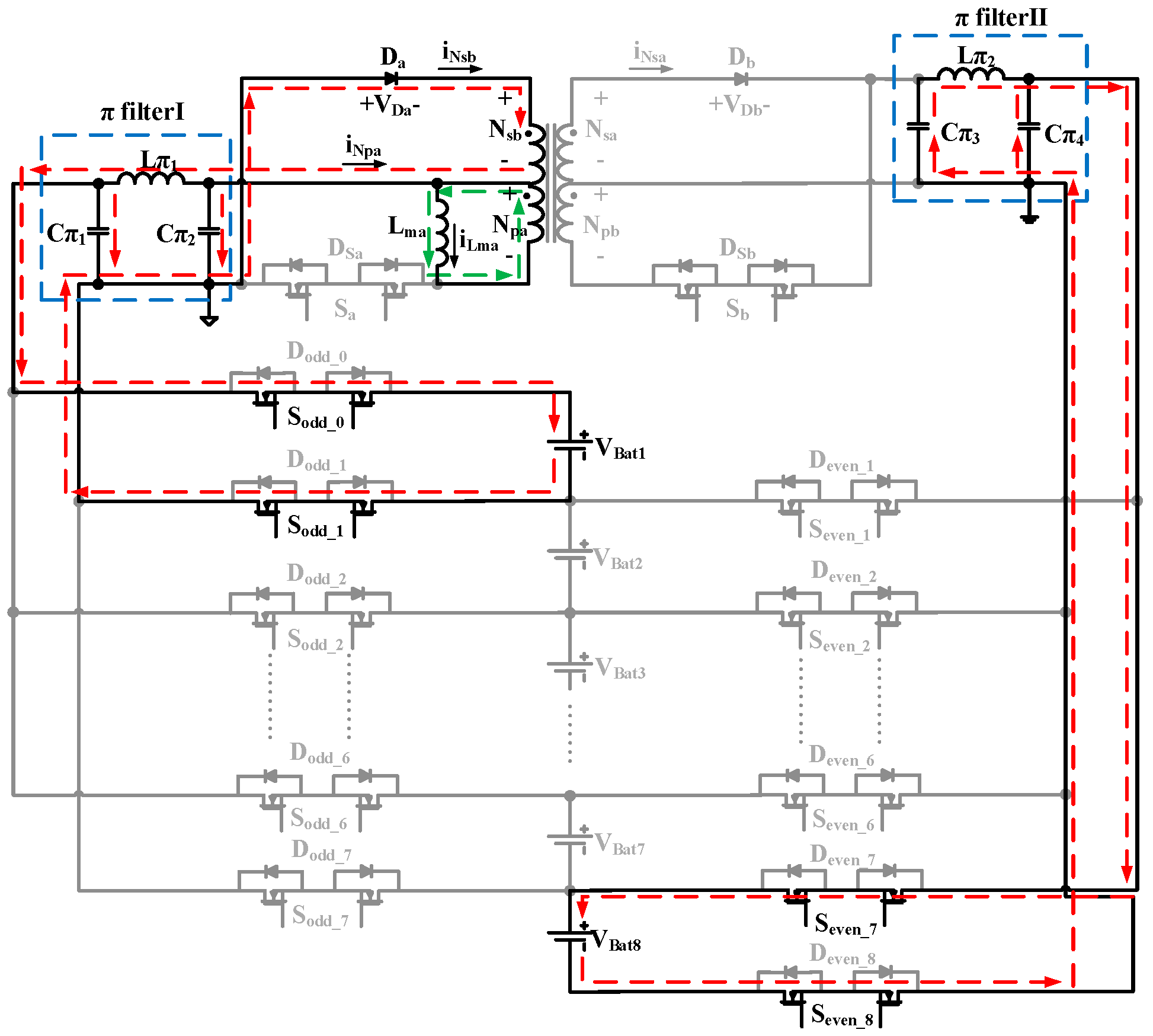
Electronics 08 01144 g003
Figure 4. Mode II, the battery balancing process from higher VBat1 to lower VBat8.
Electronics 08 01144 g004
Figure 5. The theoretical waveforms in balancing process from VBat8 to VBat1.
Electronics 08 01144 g005
Figure 6. Mode III, the battery balancing process from higher VBat8 to lower VBat1.
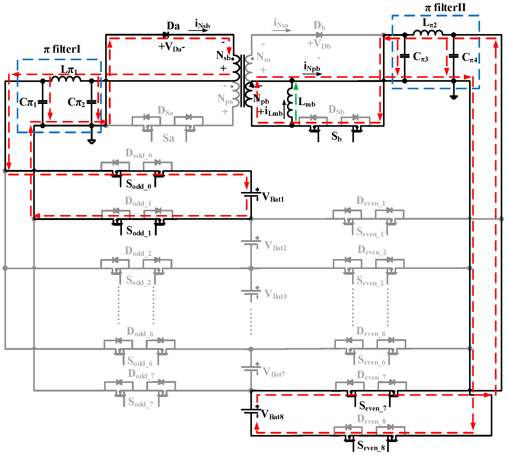
Electronics 08 01144 g006
Figure 7. Mode II, the battery balancing process from higher VBat8 to lower VBat1.
Electronics 08 01144 g007
Figure 8. Determine turns ratio by voltage of charging behavior.
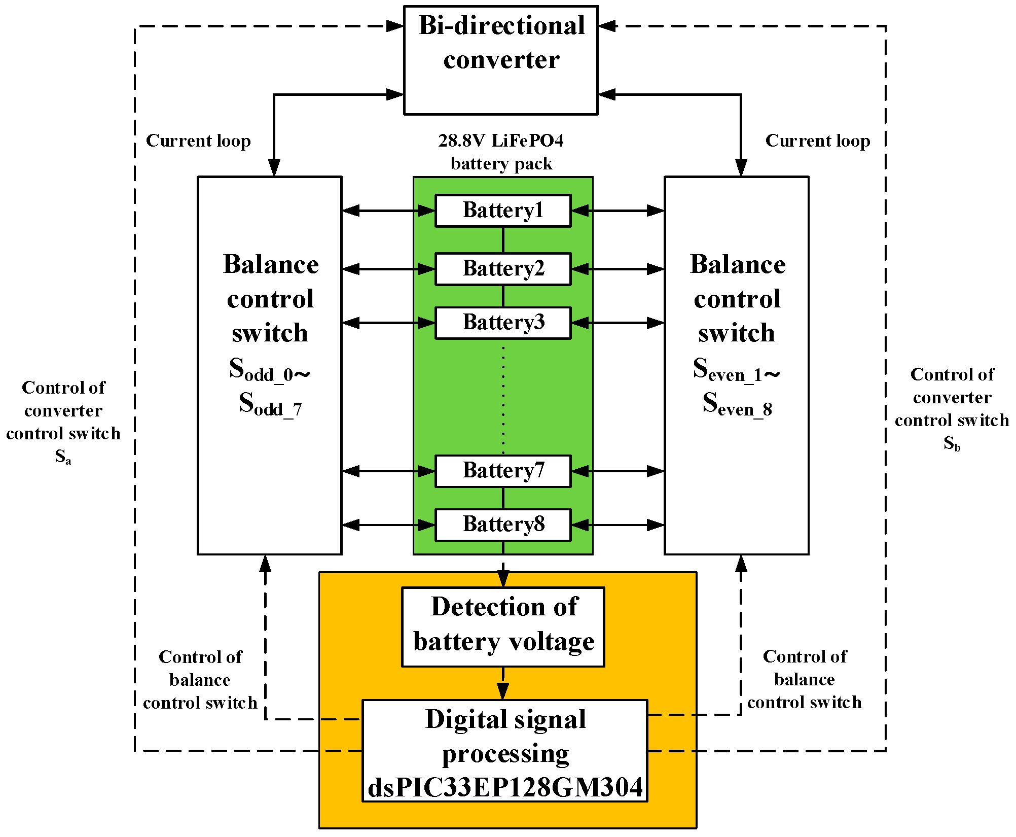
Electronics 08 01144 g008
Figure 9. The structure of fast charging balancing circuit.
Electronics 08 01144 g009
Figure 10. Flow chart of dynamic battery charging balancing strategy.
Electronics 08 01144 g010
Figure 11. The detection of battery voltage circuit.
Electronics 08 01144 g011
Figure 12. Experiment of VGS triggering waveforms for turning on the switch network (VGSodd_0, VGSodd_1, VGSeven_7, VGSeven_8), VGSodd_0, VGSodd_1, VGSeven_7, VGSeven_8: 10 V/div, Time: 20 µs/div.
Electronics 08 01144 g012
Figure 13. Experiment of voltage waveforms of Sa (VGSa, VDSa), VGSa, VDSa: 10 V/div, Time: 20 µs/div.
Electronics 08 01144 g013
Figure 14. Simulation of voltage waveforms of Sa (VGSa, VDSa), VGSa, VDSa: 10 V/div, Time: 20 µs/div.
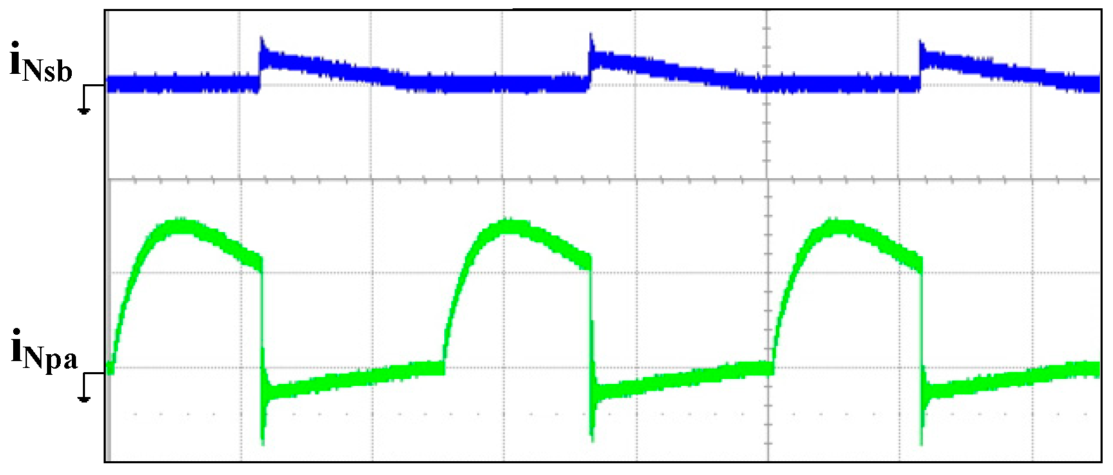
Electronics 08 01144 g014
Figure 15. Experiment of current waveforms (iNsb, iNpa), iNsb, iNpa: 500 mA/div, Time: 20 µs/div.
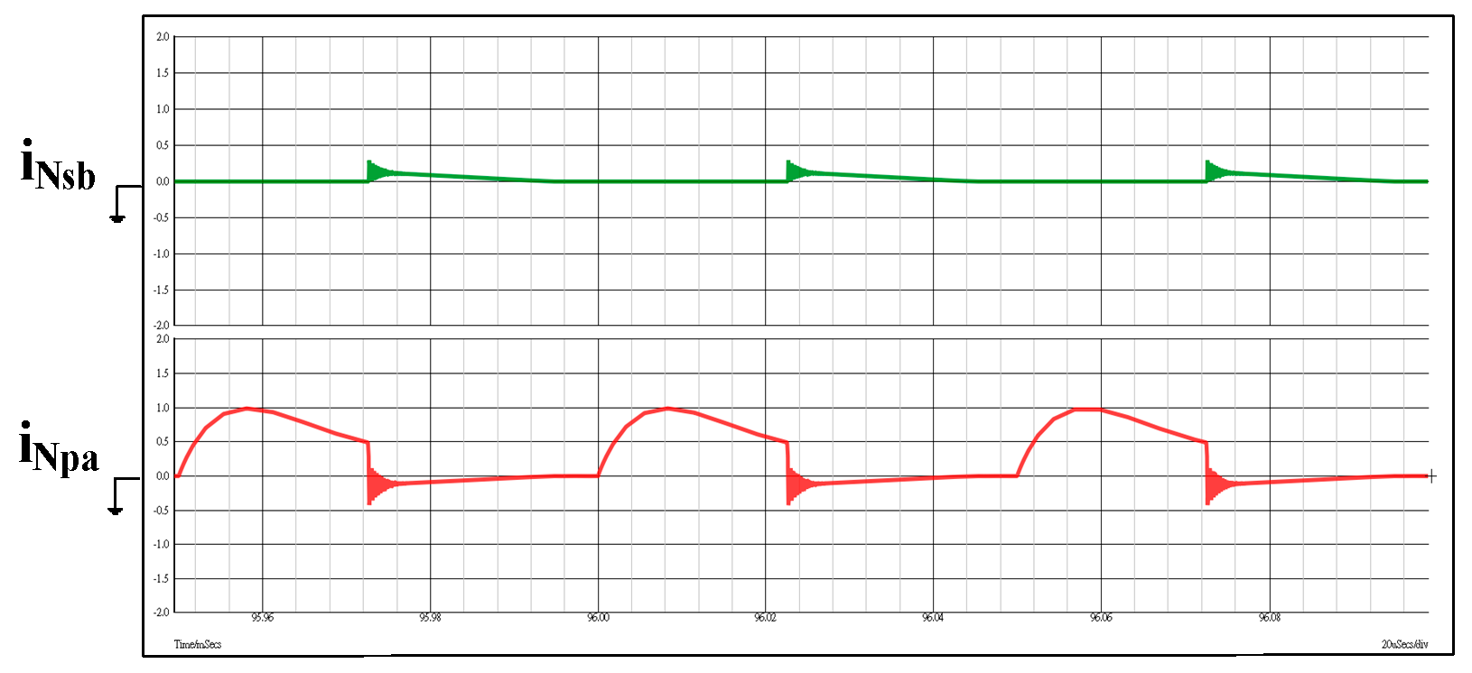
Electronics 08 01144 g015
Figure 16. Simulation of current waveforms (iNsb, iNpa), iNsb, iNpa: 500 mA/div, Time: 20 µs/div.
Electronics 08 01144 g016
Figure 17. Experiment of VGS triggering waveforms for the switch network (VGSodd_0, VGSodd_1, VGSeven_7, VGSeven_8), VGSodd_0, VGSodd_1, VGSeven_7, VGSeven_8: 10 V/div, Time: 20 µs/div.
Electronics 08 01144 g017
Figure 18. Experiment of voltage waveforms of Sb (VGSb, VDSb), VGSb, VDSb: 10 V/div, Time: 20 µs/div.
Electronics 08 01144 g018
Figure 19. Simulation of voltage waveforms of Sb (VGSb, VDSb), VGSb, VDSb: 10 V/div, Time: 20 µs/div.
Electronics 08 01144 g019
Figure 20. Experiment of current waveforms (iNsa, iNpb), iNsa, iNpb: 500 mA/div, Time: 20 µs/div.
Electronics 08 01144 g020
Figure 21. Simulation of current waveforms (iNsa, iNpb), iNsa, iNpb: 500 mA/div, Time: 20 µs/div.
Electronics 08 01144 g021
Figure 22. Battery’s voltage curve during fast charging balancing process.
Electronics 08 01144 g022
Table 1. Experimental design parameters.
Design ParametersValue
Switching Frequency fs20 kHz
Duty Cycle D45%
Turns Ratio Npa: Npb: Nsa: Nsb1: 1: 1.2: 1.2
Filtering Capacitance Cπ1, Cπ2, Cπ3, Cπ4100 µF
Filtering Inductance Lπ1, Lπ233 µH
Table 2. Specification of cell, (Company: A123 System LiFePO4 ).
Model NumberANR26650M1B
Charging Voltage3.6 V
Nominal Voltage3.3 V
Nominal Capacity2.5 Ah
Operating Temperature −30 °C~55 °C
Storage Temperature−40 °C ~60 °C
Table 3. Open loop voltage for discharged cells in the test battery string.
Cell NumberOpen Loop Voltage (V)
VBat1,(Cell1)2.623
VBat2,(Cell2)2.616
VBat3,(Cell3)2.592
VBat4,(Cell4)2.602
VBat5,(Cell5)2.611
VBat6,(Cell6)2.625
VBat7,(Cell7)2.634
VBat8,(Cell8)2.639
Table 4. Balancing time and energy loss in each interval.
Balancing IntervalBalancing Time (sec.)Energy Losses (J)
I12427.42
II17942.94
III17842.697
IV9022.012
V316.989
VI8811.391
VII409.395
Table 5. Measurement of battery balancing process.
△V1 = 0.03 V (from I–V), △V2 = 0.02 V(from V–II)Value
Total balancing time (sec.)730
Charging time (sec.)4250
Total energy loss (J)162.844
Average efficiency of the converter (%)79.8
Maximum differential voltage (V)0.018
Table 6. Comparison of different single △V for a complete balancing process.
△V (V)Total Balancing Time (sec.)Maximum Differential Voltage (V)
0.0226950.014
0.034110.023
0.043650.038
0.053150.061

