Article

High-Linearity Self-Biased CMOS Current Buffer

by
Javier Alejandro Martínez-Nieto
1,*,
María Teresa Sanz-Pascual
1,
Nicolás Medrano-Marqués
2,
Belén Calvo-López
2 and
Arturo Sarmiento-Reyes
1
1
Electronics Department, National Institute of Astrophysics, Optics and Electronics (INAOE), 72840 Puebla, Mexico
2
Group of Electronic Design (GDE), University of Zaragoza, 50009 Zaragoza, Spain
*
Author to whom correspondence should be addressed.
Electronics 2018, 7(12), 423; https://doi.org/10.3390/electronics7120423
Submission received: 7 November 2018 / Revised: 3 December 2018 / Accepted: 6 December 2018 / Published: 11 December 2018
(This article belongs to the Special Issue Signal Processing and Analysis of Electrical Circuit)

Abstract

:
A highly linear fully self-biased class AB current buffer designed in a standard 0.18 μ m CMOS process with 1.8 V power supply is presented in this paper. It is a simple structure that, with a static power consumption of 48 μ W, features an input resistance as low as 89 Ω , high accuracy in the input–output current ratio and total harmonic distortion (THD) figures lower than −60 dB at 30 μ A amplitude signal and 1 kHz frequency. Robustness was proved through Monte Carlo and corner simulations, and finally validated through experimental measurements, showing that the proposed configuration is a suitable choice for high performance low voltage low power applications.

1. Introduction

Current mirrors are required not only to generate and replicate bias currents, but also as core cells in many analog and mixed signal applications: current conveyors, current feedback operational amplifiers or current-mode filters, among others, are based on this basic current processing block [1,2,3,4,5,6,7,8,9]. Unfortunately, the power consumption of current-mode circuits proportionally increases as the number of active branches where the current is replicated increases. This limitation, critical for the current low-voltage low-power IC design scenario set by the driving portable market, can be circumvented through class AB operation, which makes it possible to dynamically handle current levels higher than the quiescent bias current [10,11,12,13,14]. Furthermore, self-biasing may be used to establish the DC current in the circuit without any additional bias circuitry in order to optimize the power consumption [15].
The goal of this work is to accomplish a reliable fully self-biased class AB current buffer design. It relies on an active input to attain very low input impedance and high linearity, which is further increased by the coupling of the input and output branches through a single transistor. Preliminary results from a not fully self-biased implementation, i.e., requiring extra bias generation for the cascode transistors and the input amplifier, are presented in [16]. This paper presents the complete fully self-biased design, providing more insight into the operation principle and the actual implementation of the required amplifier and the corresponding compensation network, considering both a single-stage and a two-stage differential amplifier. Simulations including process variations and mismatch effects, as well as experimental results, validate the reliability of the proposed approach.
The circuit was characterized and compared with two other widely used class AB buffers designed with the same technology, same power supply and for the same input current range. The first is a quasi-floating gate current buffer (QFG-CB) and the second is a current-conveyor based current buffer (CC-CB). These topologies were chosen for their class AB operation as well as for their ability to keep the input node at a constant DC input voltage V d c (virtual ground), as the proposed circuit does. This is a desirable characteristic in many cases, and becomes essential in some particular configurations based on MOS current dividers [17,18,19]. A particular case where this feature is exploited is the sign circuit required within the neuron of an analog neural system used to calibrate sensors [20,21] (see Figure 1). This sign circuit is required to determine the direction of the current flowing through a multiplier, thus allowing both positive and negative synaptic weights [22]. This particular application motivated the design of the proposed self-biased buffer configuration, with the key requirements of providing the highest possible accuracy and linearity response with a reduced power consumption and a compact size.
The paper is organized as follows: Section 2 presents the operation principle of the proposed buffer. The differential amplifiers and the compensation techniques used to ensure the buffer stability are also presented in this section. In Section 3, the current buffer is thoroughly characterized for both a single-stage and a two-stage amplifier as active input components to show the corresponding trade-offs. A comparison with two other widely used class AB current buffers with a well defined input voltage is also made. Measurement results of the integrated current buffer prototype and a comparison with other integrated circuits are presented in Section 4 and, finally, conclusions are drawn in Section 5.

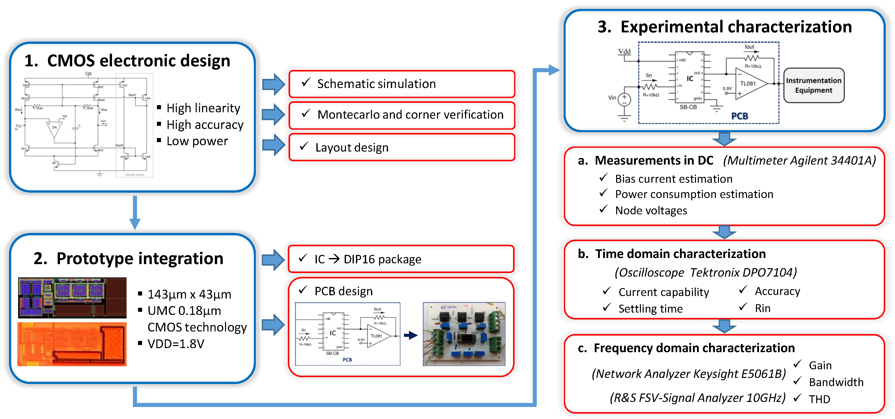
2. Proposed Self-Biased Current-Buffer

The proposed self-biased current buffer (SB-CB) is shown in Figure 2. A Differential Amplifier (DA) sets the input voltage at V d c and establishes a virtual ground at this node. The quasi-floating gate (QFG) approach is used to achieve class AB operation [23,24,25,26,27,28,29,30], since this technique requires no additional current and adds minimum hardware penalty, leading to a power efficient and compact solution. In static conditions, the bias current I B i a s is determined by the dimensions of the PMOS (P-type metal-oxide-semiconductor) transistors M p 1 and M p 2 , which are diode-connected and equally sized. Therefore, the same current flows through each NMOS (N-type metal-oxide-semiconductor) transistor M n 1 and M n 2 , whereas M 1 sinks twice the bias current.
Under dynamic conditions, the PMOS transistors act as dynamic current sources. If the input current flows out of the buffer, the current flowing through M n 1 and M n 2 decreases and so does the tail current in transistor M 1 . Due to the RC coupling formed by capacitance C and resistances R l a r g e , the gate voltage of M p 1 and M p 2 drops and their current driving capability increases. Hence, the bias current of the buffer is lower than the input current that can be handled. Neglecting channel-length modulation, the current transfer function is given by:
I o u t I i n = ( g m n 1 + g m n 2 ) g m p 2 + A d g m 1 g m n 2 ( g m n 1 + g m n 2 ) g m p 1 + A d g m 1 g m n 1
where A d is the gain of the differential amplifier and g m i is the transconductance of transistor M i . If a unity current gain, i.e., a current buffer, is required, the transconductance ratios g m p 2 / g m p 1 and g m n 2 / g m n 1 must both be equal to 1.
The input resistance R i n is the parallel of the equivalent resistance R i n P seen from the input to V D D , and the equivalent R i n N seen from the input to ground:
R i n P = g m c p 1 r o c p 1 r o p 1 1 + g m p 1 r o c p 1 ( g m c p 1 r o p 1 1 )
R i n N = 2 r o n 1 1 + A d g m 1 r o n 1
R i n = R i n P R i n N 2 2 g m p 1 + A d g m 1
As expected, R i n can be reduced by increasing the differential amplifier gain A d . The output resistance R o u t is given by:
R o u t = 2 g m p 1 2 r o n 1 + 1 g m 1 2 g m p 1
R o u t is dominated by the equivalent resistance of the diode connection of transistor M p 1 , so it may be lower than in other current buffer implementations. However, as shown below, a 2.4 M Ω output resistance was achieved in our design, which is still suitable for many applications.
The proposed SB-CB was designed in a standard 0.18 μ m CMOS process with 1.8 V supply voltage. The transistor sizes are shown in Table 1. The channel length is L 1 μ m in all cases in order to reduce mismatch effects. The sizes were chosen so the buffer would be able to handle input currents up to 15 μ A amplitude with a nominal bias current I B i a s = 8 μ A. The coupling Metal-Insulator-Metal (MIM) capacitor has a value C = 1 pF. The resistances R l a r g e were implemented with minimum-size diode-connected MOS transistors in the cutoff region [31], as they do not need to have a precise value as long as the cutoff frequency f c = 1 / [ 2 π R l a r g e C ] is lower than the signal frequency. Cascode transistors improve the accuracy in the current copy, and the self-bias scheme shown in Figure 2 was used to establish the required B i a s P and B i a s N voltages [32]. Finally, an NMOS transistor not shown in the figure was connected to the input node as start-up circuit.
To analyze the stability of the SB-CB, it must be noted that the open-loop gain is given by:
A o l = A d · A c s
where A d is the gain of the differential amplifier DA and A c s is the gain of the common-source stage, i.e., transistor M 1 :
A c s g m 1 · 1 + 2 g m p 1 r o n 1 2 g m p 1 ( 1 + g m p 1 r o n 1 )
First, a current buffer SB-CB1 where the DA is a single-stage PMOS differential pair with active load will be considered. When opening the feedback loop, a two-stage configuration results, as shown in Figure 3. To ensure stability, Miller compensation is applied. The bias current is set to 500 nA and derived from the current buffer itself. The amplifier shows 40 dB gain and the buffer is compensated with a Miller capacitance C c o m p = 300 fF, attaining 82 phase margin for B W = 4.1 MHz.
As shown in Equation (4), a higher gain differential amplifier will decrease the input impedance. Furthermore, the linearity is expected to increase by the virtual ground set at the input node. Therefore, a two-stage amplifier was also designed to explore the impact of the amplifier on the overall performance of the buffer. If the DA is a two-stage amplifier, the open-loop configuration turns into a three-stage amplifier, as shown in Figure 4. To achieve stability, nested-Miller compensation can be applied. This technique requires the second stage in the differential amplifier not to invert the signal, so the amplifier has to be accordingly designed [33,34,35].
As shown in Figure 4, the two-stage DA was implemented with two cascaded PMOS differential pairs. An additional differential pair, not shown in the figure, was used to set the required bias voltage V b i a s at the negative input of the second stage so the current distribution through its branches is symmetrical. Again, the bias currents were derived from the current buffer itself. Each differential pair is biased with 500 nA and the two-stage DA gain is 78 dB. The compensation capacitors values are C C 1 = 400 fF and C C 2 = 100 fF. The phase margin with the nested-Miller compensation is P M = 62 for a bandwidth (BW) of 3 MHz.

3. Performance Characterization

For the sake of comparison, simulations were carried out for the self-biased buffer both with a single-stage amplifier (SB-CB1) and a two-stage amplifier (SB-CB2) as DA.
Figure 5 shows the output current and the relative error in the copy of current as a function of the input current. The SB-CB2 shows lower relative error in the transfer current. Considering a minimum input current I i n = 100 nA, the maximum relative error is 0.09 % for the SB-CB2 and 0.24 % for the SB-CB1. If the minimum input current is reduced to I i n = 10 nA, the maximum relative error increases to 0.75 % for the SB-CB2 and 2.08 % for the SB-CB1.
As for linearity, both current buffers show very low harmonic distortion. The THD for a 15 μ A amplitude input current remains below −60 dB up to 100 kHz for the SB-CB2 and up to 30 kHz for the SB-CB1. Figure 6 shows THD versus frequency for both configurations.
Figure 7 shows the time response to a 30 μ A pp input current step for both SB-CBs. For the SB-CB1, the rise time is 1.23 μ s and the fall time is 898 ns, both considering the response within 0.1 % of the output signal. As for the SB-CB2 the rise time is 947 ns and the fall time is 1.13 μ s under the same conditions.
Table 2 summarizes the main electrical characteristics of the proposed buffers SB-CB1 and SB-CB2. As expected, SB-CB2 shows higher linearity and lower input resistance than SB-CB1 with a slight increment in power consumption. Table 2 also shows the characteristics of two other widely used class AB current buffers with a virtual ground at the input node. For a fair comparison, these buffers were redesigned in the same 0.18 μ m CMOS process with 1.8 V supply and for the same input current range I i n = ± 15 μ A.
The Quasi-Floating Gate Current-Buffer (QFG-CB) is presented in [26] and, as in the proposed SB-CB, the bias transistors act as dynamic current sources. The two-stage differential amplifier shown in Figure 4 was used in the design of the QFG-CB, and, again, nested-Miller compensation was used to ensure stability. The second configuration considered for comparison is the Current Conveyor based Current Buffer (CC-CB) [36,37,38,39,40,41]. Figure 8 shows both the schematic circuits and the transistor sizes of the aforementioned class AB current buffers. According to Table 2, the QFG-CB and the proposed circuit have higher estimated active area than the CC-CB due the MIM capacitors used for the QFG technique. However, if only the number of transistors is considered, the proposed circuit has the smallest area.
The bias current I B i a s is lowest for the QFG-CB, which results in the lowest power consumption, both static and dynamic. However, it should be mentioned that both the QFG-CB and CC-CB require additional biasing schemes which are not considered in the comparison.
The QFG-CB and the proposed SB-CB2 show the lowest relative error in the copy of current. At an input current I i n = 100 nA, the relative error remains below 0.1 % for both circuits, and, even considering an input current I i n = 10 nA, the relative error remains below 0.8 % in both cases, whereas the error of the CC-CB rises to 45 % , which is unbearable in practical cases. As for the THD@ 30 μ A pp , it remains below −60 dB up to 100 kHz both for the SB-CB2 and for the QFG-CB. The CC-CB, in contrast, shows a THD higher than −55 dB even at low frequencies.
The proposed buffer shows the lowest input resistance, thanks both to the negative feedback established by the amplifier and to the diode-connection of the PMOS transistors. However, as expected, it also shows the lowest output resistance. A transistor working in saturation could be added in series with the diode-connected transistor to increase R o u t . To keep the circuit symmetry, it would be necessary to also add another transistor to the input branch, but, from Equations (2)–(4), it can be seen that the input resistance may still be very low as long as the amplifier gain is sufficiently high. Finally, the proposed buffer shows the highest bandwidth.
To prove the robustness of the proposed self-biased buffers, corner process simulations were carried out and Table 3 shows the results. To ensure proper operation under all conditions, even when the bias current is reduced because of process variations, the transistors M p 1 and M p 2 were oversized in the design stage. The bias current I B i a s decreases down to 6.5 μ A in the slow-slow corner but performance is not affected and the THD for a 30 μ A pp input current at 1 kHz remains below −80 dB for all cases. In the fast-fast corner, I B i a s increases up to 10 μ A, therefore increasing the total power consumption to 38.7 μ W for the SB-CB1 and 41.6 μ W for the SB-CB2. As for the QFG-CB and CC-CB topologies, their robustness to process variations depends on the robustness of the external biasing circuit.
Finally, Monte Carlo simulations were carried out to verify the circuit operation under mismatch. The mean value and the standard deviation of main electrical parameters considering 500 samples are summarized in Table 4. In the proposed buffers, SB-CB1 and SB-CB2, the mean value for the gain distribution is practically 1 with the same 0.7 % standard deviation. The SB-CB1 shows a higher mean offset value than SB-CB2, but the latter presents a higher standard deviation. As for THD, the mean value is lower than −66 dB for both circuits considering a 15 μ A amplitude and 1 kHz frequency input signal. Linearity is therefore primarily degraded by mismatch and, according to these results, the actual THD is almost the same for the single-stage and the two-stage implementations. The SB-CB2 implementation may still be preferred if a very low input resistance is required, as is the case for example in configurations based on MOS current dividers [17,18]. Table 4 also shows that I B i a s is very robust to mismatch variations, and therefore so is the overall power consumption.
By comparing the proposed SB-CB2 with the two other buffers, results show that the three implementations have a mean value in gain of nearly 1, showing the CC-CB the lowest standard deviation and the SB-CB2 the highest. The proposed SB-CB2 and the QFG-CB show similar offset mean value, but the SB-CB2 shows again the highest standard deviation. In Figure 9 the THD distribution is represented for all three implementations. The CC-CB shows the worst mean value of THD but the lowest standard deviation. The proposed self-biased buffer, in turn, is the most sensitive to mismatching, but still shows the highest linearity.

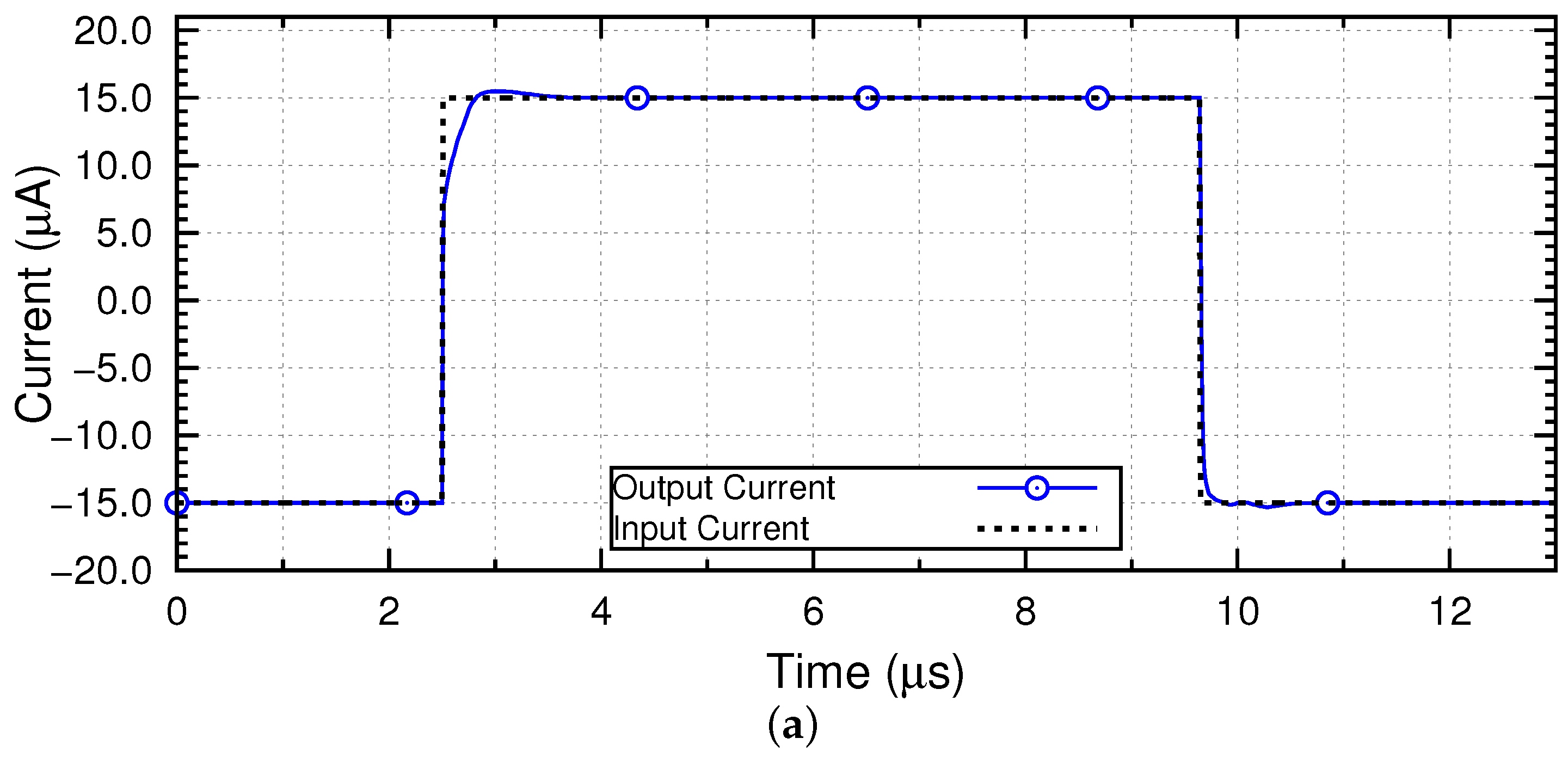
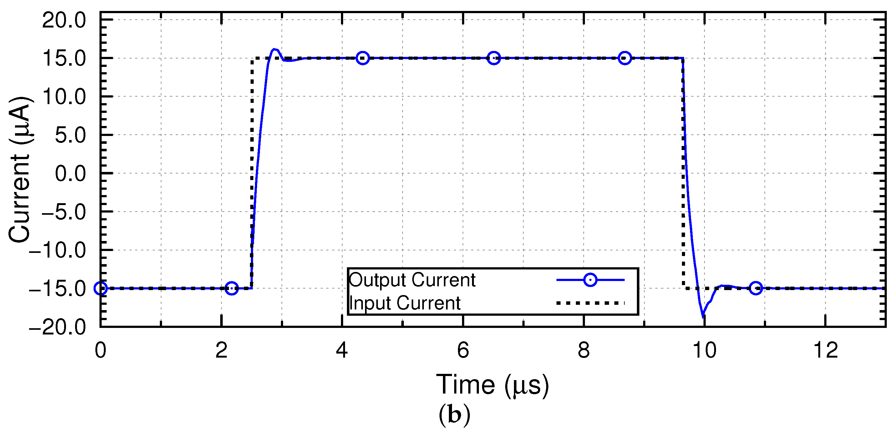
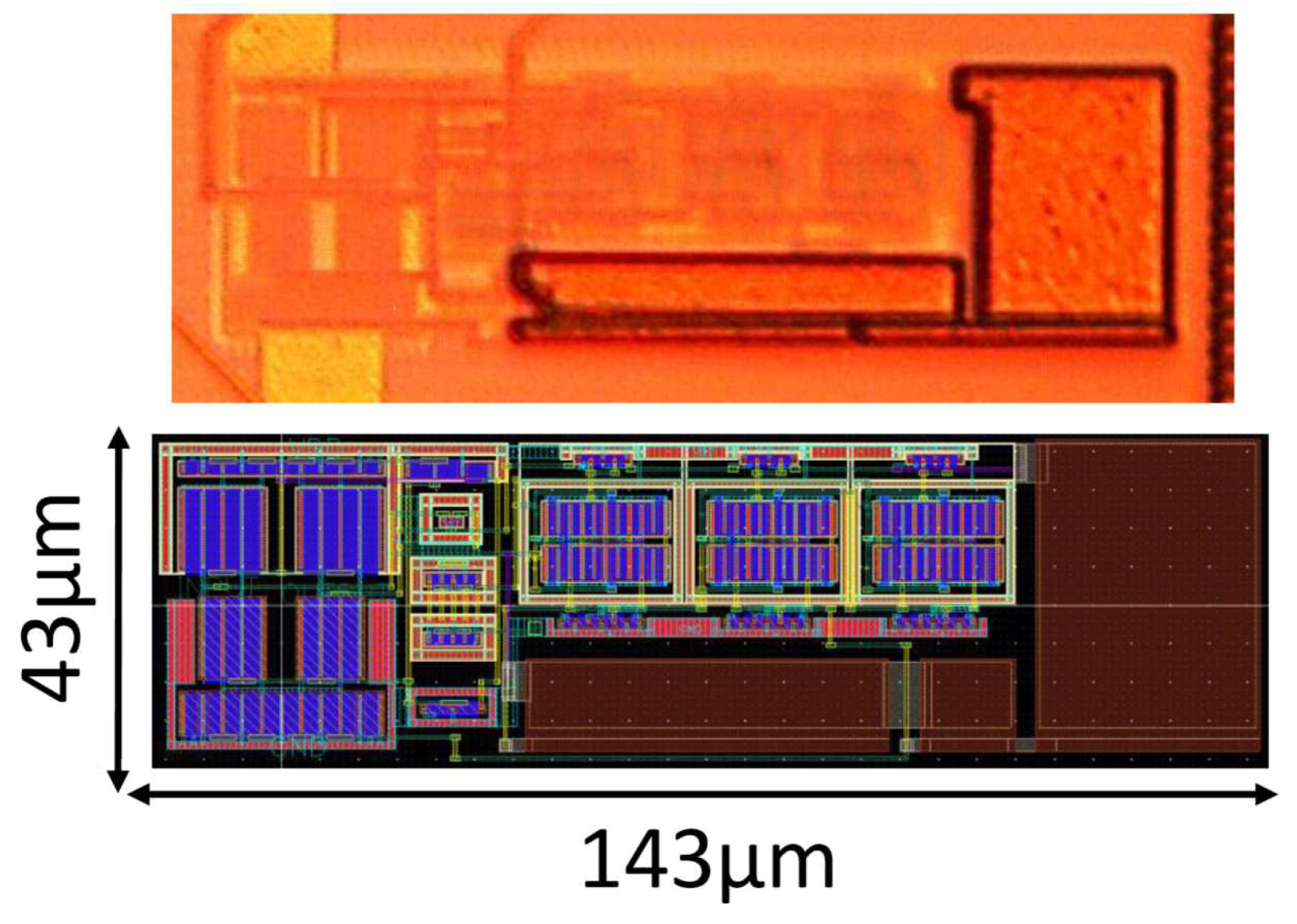
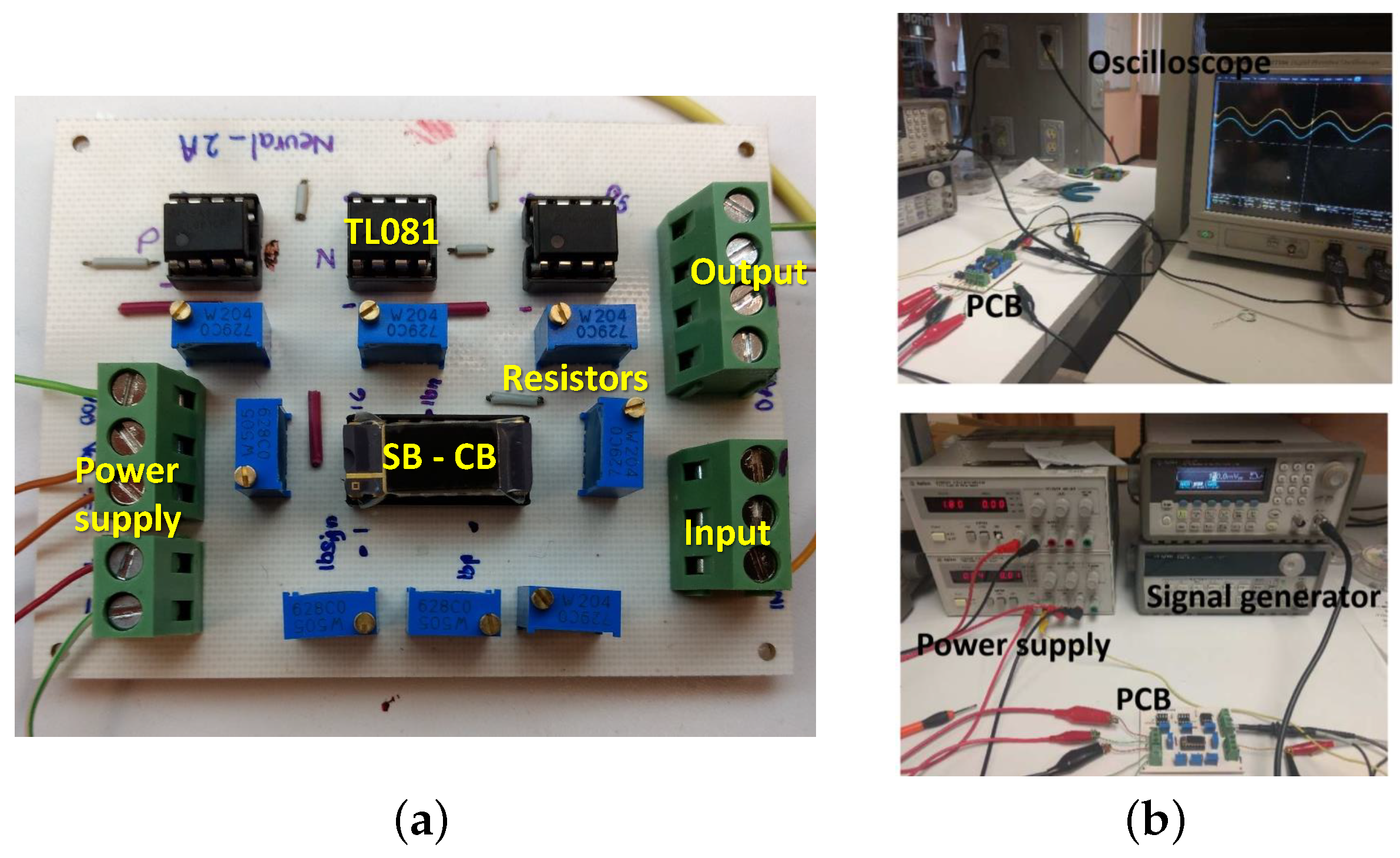
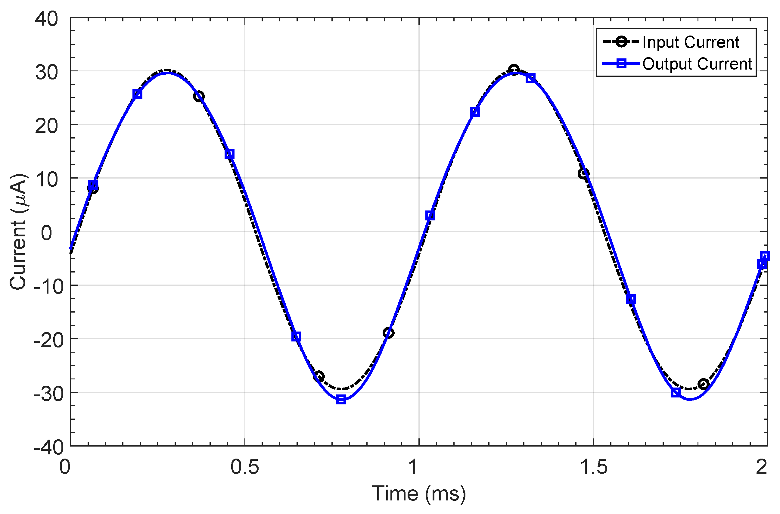
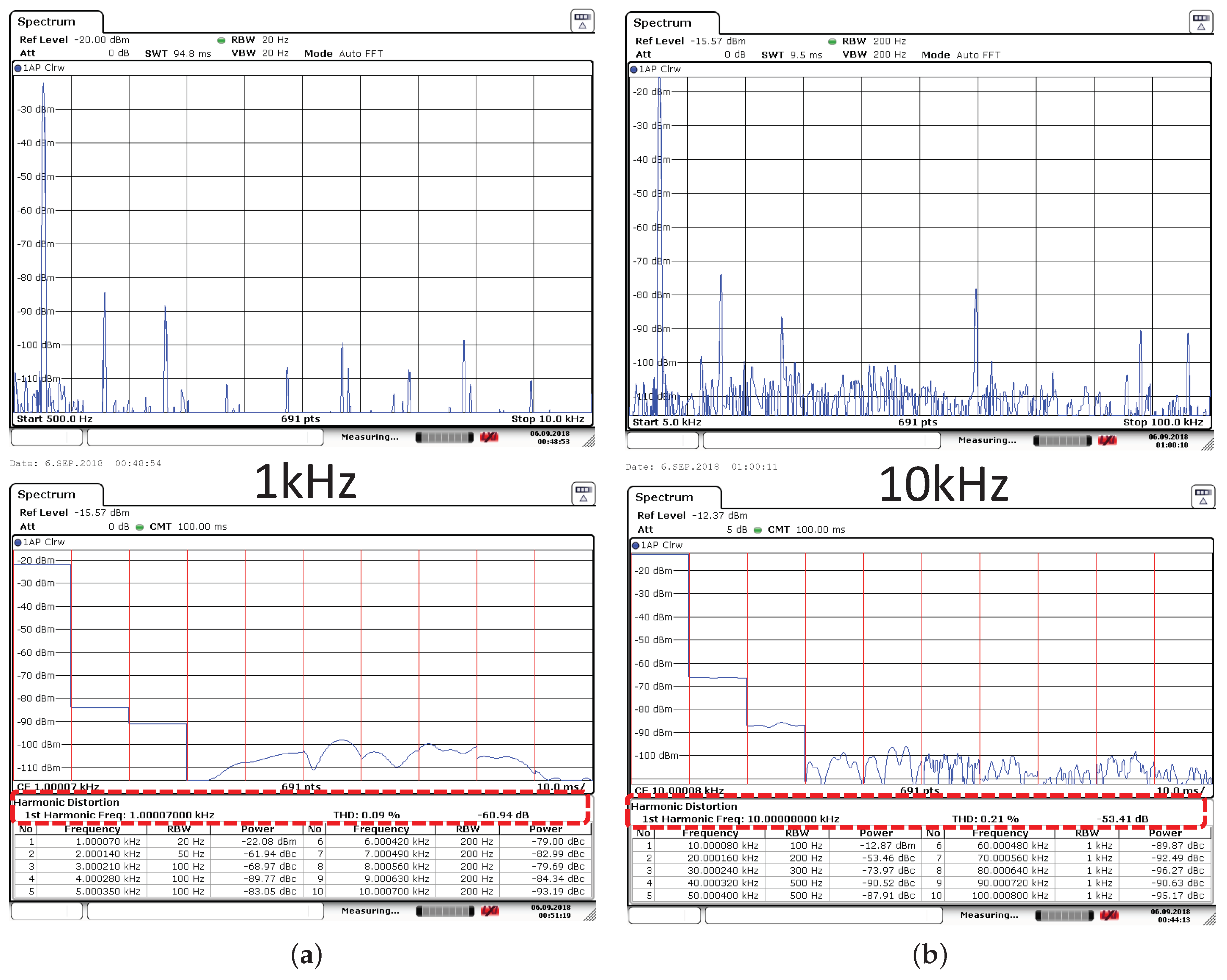
4. Experimental Results

The self-biased current buffer SB-CB2 was integrated in the UMC (United Microelectronics Corporation) 0.18 μ m CMOS technology with 1.8 V power supply. Figure 10 shows the microphotograph of the circuit and the layout. The circuit implementation occupies an area of 143 μ m × 43 μ m and exhibits a power consumption of 48 μ W. Accordingly, the bias current is estimated to be 12 μ A, which is a bit higher than expected from the results in Table 3. This increase in the bias current in turn results in an increase in the current capability of the buffer.
A PCB (Printed Circuit Board) was designed to carry out the characterization process. Figure 11a shows this PCB, and Figure 11b shows the photograph of the test setup. As the circuit processes the signal in the current domain, current conversion is necessary at both the input and the output. By means of a 10 k Ω resistance connected at the input node, the input current was generated, whereas the output current was measured through an external transimpedance amplifier configured with a TL081 integrated circuit [42]. This is detailed in Figure 12, which shows a block diagram of the interconnections within the PCB, as well as the methodology followed to carry out the experimental measurements after the circuit has been fabricated.
First, the current buffer was characterized under static conditions to obtain the DC characteristics and verify that the prototype is properly biased. Then, the time response was observed in the oscilloscope to test the current capability and accuracy of the buffer, as well as the settling time and input resistance. Finally, the frequency response and the harmonic distortion were characterized.
The circuit response to a 60 μ A pp sine input current at 1 kHz frequency is shown in Figure 13. This is the maximum output current that the buffer can handle before the signal starts getting distorted. The input–output characteristic is shown in Figure 14 for a 30 μ A to + 30 μ A current range. A maximum relative error e r = 1.35 % is obtained, as also shown in Figure 14.
The input resistance was estimated from the response in the time domain, by measuring the input node voltage and calculating the derivative with respect to the input current. A 89 Ω input resistance was obtained.
If a 60 μ A pp input current step is considered, the circuit shows a rise time of 8.6 μ s and a fall time of 8.4 μ s, both considering the response within 0.1 % of the output signal. Figure 15 shows the oscilloscope screenshots of the buffer response to both the rising and falling edges of the input step for this dynamic characterization.
The THD characterization was done using the signal analyzer ROHDE & SCHWARZ FSV-Signal Analyzer (10 Hz–6 GHz) [43]. Figure 16 shows the spectrum analyzer screenshots when considering a 60 μ A pp sine input signal at 1 kHz (Figure 16a) and 10 kHz (Figure 16b). Both the frequency spectrum and the THD calculation are shown, considering ten harmonic components. The integrated prototype shows a −61 dB THD for the 60 μ A pp input current at 1 kHz, and −53 dB at 10 kHz. These values correspond to the distortion specifications of the signal generator, so lower distortion values are actually expected.
Finally, the transfer function in the frequency domain was determined using the network analyzer E5061B ENA [44], as shown in Figure 17. Note that the bandwidth was reduced because of the parasitic capacitances of the chip package and the interconnection setup used for the characterization.
The self-biased current buffer electrical characteristics are summarized in Table 5, where a comparison with other topologies found in the literature is also presented. All the buffers presented in the table are based on the quasi-floating gate technique.
Note that, although the proposed circuit requires the highest bias current, it does not have a significant impact on the final consumption. Furthermore, the bias circuit of the other topologies has not been considered when estimating their power consumption.
The buffer in [26] and the proposed circuit show the lowest input resistance of 25 Ω and 89 Ω , respectively, so that a virtual ground is set at the input node, and therefore a higher linearity is observed when the maximum input current is considered in each case. The best experimental distortion figure is obtained in [26], at the cost of increased power consumption, which is almost three times the proposed SB-CB consumption. The buffers in [28,29] both present competitive power consumption, but with a rather high R i n ( 934 Ω and 4.8 k Ω , respectively). A higher distortion of −40 dB is observed in [28] for the maximum input current; even if a lower input current of 30 μ A amplitude is considered, the THD is not higher than −53 dB. Similarly, the buffer presented in [29] shows a THD of −41 dB for a current I i n = 100 μ A pp .
Finally, the proposed SB-CB shows the lowest integration area, whereas the circuit presented in [29] has the highest dimensions because it uses three capacitors to achieve the class-AB operation.

5. Conclusions

A self-biased class AB 1.8 V–0.18 μ m CMOS current buffer based on the QFG approach is proposed in this paper. It shows the lowest input resistance and highest linearity when compared to other class AB current buffers with a virtual ground at the input node, at a cost of higher power consumption. However, as the proposed topology is self-biased, it does not require any additional circuitry, whereas other buffers require a biasing scheme. Monte Carlo and process corner simulations show that, even though the proposed buffer is more sensitive to process variations, it still shows the best performance in terms of linearity.
The integrated prototype was able to copy an input current ranging from 30 μ A to + 30 μ A with a maximum relative error of 1.35 % and 48 μ W static power consumption. The prototype has a reduced area of 143 × 43 μ m 2 , making it a viable solution for battery-operated systems where minimum dimensions and low power operation are mandatory. The THD for the same amplitude input current remains below −53 dB up to 10 kHz, showing a high linearity characteristic even when the maximum input current is considered. The circuit also has a very low input resistance R i n = 89 Ω , thus setting a virtual ground at the input node, a relatively high output impedance and a circuit response time of 8.6 μ s.

Author Contributions

Conceptualization, J.A.M.-N., M.T.S.-P. and B.C.-L.; Methodology, J.A.M.-N., M.T.S.-P. and A.S.-R.; Investigation, J.A.M.-N. and M.T.S.-P.; Validation, J.A.M.-N. and N.M.-M.; Writing—Original draft preparation, J.A.M.-N.; Writing—review and editing, J.A.M.-N., M.T.S.-P., N.M.-M., B.C.-L. and A.S.-R.; and Supervision, M.T.S.-P. and N.M.-M.

Funding

This work was supported by CONACYT 362674 Ph.D. Grant, CONACYT project No. CB-2015-257985 and MINECO-FEDER, UE (TEC2015-65750-R) Research Project.

Conflicts of Interest

The authors declare no conflict of interest. The founding sponsors had no role in the design of the study; in the collection, analyses, or interpretation of data; in the writing of the manuscript, and in the decision to publish the results.

References

  1. Kumgern, M.; Wareechol, E.; Phasukkit, P. Quadrature oscillator and universal filter based on translinear current conveyors. AEU Int. J. Electron. Commun. 2018, 94, 69–78. [Google Scholar] [CrossRef]
  2. Cini, U. A low-offset high CMRR current-mode instrumentation amplifier using differential difference current conveyor. In Proceedings of the 2014 21st IEEE International Conference on Electronics, Circuits and Systems (ICECS), Marseille, France, 7–10 December 2014; pp. 64–67. [Google Scholar] [CrossRef]
  3. Esparza-Alfaro, F.; Pennisi, S.; Palumbo, G.; Lopez-Martin, A. Low-power class-AB CMOS voltage feedback current operational amplifier with tunable gain and bandwidth. IEEE Trans. Circuits Syst. II Express Briefs 2014, 61, 574–578. [Google Scholar] [CrossRef]
  4. Swamy, M.N.S. Modified CFOA, its transpose, and applications. Int. J. Circuit Theory Appl. 2016, 44, 514–526. [Google Scholar] [CrossRef]
  5. Reshma, P.G.; Gopi, V.P.; Babu, V.S.; Wahid, K.A. Analog CMOS implementation of FFT using cascode current mirror. Microelectron. J. 2017, 60, 30–37. [Google Scholar] [CrossRef]
  6. Tsirimokou, G.; Psychalinos, C. Ultra-low voltage fractional-order circuits using current mirrors. Int. J. Circuit Theory Appl. 2016, 44, 109–126. [Google Scholar] [CrossRef]
  7. Sotner, R.; Jerabek, J.; Langhammer, L.; Dvorak, J. Design and Analysis of CCII-Based Oscillator with Amplitude Stabilization Employing Optocouplers for Linear Voltage Control of the Output Frequency. Electronics 2018, 7, 157. [Google Scholar] [CrossRef]
  8. Mowlavi, S.; Baharmast, A.; Sobhi, J.; Koozehkanani, Z. A novel current-mode low-power adjustable wide input range four-quadrant analog multiplier. Integration 2018, 63, 130–137. [Google Scholar] [CrossRef]
  9. Lopez-Martin, A.; Garde, M.P.; Carvajal, R.G.; Ramírez-Angulo, J. On the Optimal Current Followers for Wide-Swing Current-Efficient Amplifiers. In Proceedings of the IEEE International Symposium on Circuits and Systems (ISCAS), Florence, Italy, 27–30 May 2018; pp. 1–5. [Google Scholar] [CrossRef]
  10. Lopez-Martin, A.J.; Acosta, L.; Garcia-Alberdi, C.; Carvajal, R.G.; Ramirez-Angulo, J. Power-efficient analog design based on the class AB super source follower. Int. J. Circuit Theory Appl. 2012, 40, 1143–1163. [Google Scholar] [CrossRef]
  11. Pourashraf, S.; Ramírez-Angulo, J.; Lopez-Martin, A.J.; González-Carvajal, R. A super class-AB OTA with high output current and no open loop gain degradation. In Proceedings of the IEEE 60th International Midwest Symposium on Circuits and Systems (MWSCAS), Boston, MA, USA, 6–9 August 2017; pp. 815–818. [Google Scholar]
  12. Bruschi, P.; Navarrini, D.; Piotto, M. A class-AB CMOS operational amplifier for application as rail-to-rail high current drive output buffer. In Proceedings of the 28th European Solid-State Circuits Conference (ESSCIRC), Florence, Italy, 24–26 September 2002; pp. 731–734. [Google Scholar]
  13. Kawahito, S.; Tadokoro, Y. CMOS class-AB current mirrors for precision current-mode analog-signal-processing elements. IEEE Trans. Circuits Syst. II Analog Digit. Signal Process. 1996, 43, 843–845. [Google Scholar] [CrossRef]
  14. Zhao, X.; Wang, Y.; Jia, D.; Dong, L. Ultra-high current efficiency single-stage class-AB OTA with completely symmetric slew rate. AEU-Int. J. Electron. Commun. 2018, 87, 65–69. [Google Scholar] [CrossRef]
  15. Grasso, A.D.; Marano, D.; Esparza-Alfaro, F.; Lopez-Martin, A.J.; Palumbo, G.; Pennisi, S. Self-biased dual-path push-pull output buffer amplifier for LCD column drivers. IEEE Trans. Circuits Syst. I Regul. Pap. 2014, 61, 663–670. [Google Scholar] [CrossRef]
  16. Martinez-Nieto, J.A.; Sanz-Pascual, M.T.; Medrano-Marques, N.J.; Calvo-Lopez, B. Self-biased class-AB CMOS current buffer. In Proceedings of the IEEE 7th Latin American Symposium on Circuits Systems (LASCAS), Florianopolis, Brazil, 28 February–2 March 2016; pp. 255–258. [Google Scholar]
  17. Bult, K.; Geelen, G. An inherently linear and compact most-only current-division technique. In Proceedings of the Solid-State Circuits Conference, Digest of Technical Papers, San Francisco, CA, USA, 19–21 February 1992; pp. 198–199. [Google Scholar] [CrossRef]
  18. Pun, K.P.; Choy, C.S.; Chan, C.F.; da Franca, J. Digital frequency tuning technique based on current division for integrated active RC filters. Electron. Lett. 2003, 39, 1366–1367. [Google Scholar] [CrossRef]
  19. Wang, W.; Jia, S.; Pan, T.; Wang, Y. Design of low-power high-speed dual-modulus frequency divider with improved MOS current mode logic. In Proceedings of the IEEE International Conference on Electron Devices and Solid State Circuits (EDSSC), Shenzhen, China, 6–8 June 2018; pp. 1–2. [Google Scholar]
  20. Martínez-Nieto, J.A.; Sanz-Pascual, M.T.; Medrano-Marqués, N.J. Integrated mixed mode neural network implementation. In Proceedings of the European Conference on Circuit Theory and Design (ECCTD), Catania, Italy, 4–6 September 2017; pp. 1–4. [Google Scholar]
  21. Martínez-Nieto, A.; Medrano, N.; Sanz-Pascual, M.T.; Calvo, B. An accurate analysis method for complex IC analog neural network-based systems using high-level software tools. In Proceedings of the IEEE 9th Latin American Symposium on Circuits & Systems (LASCAS), Puerto Vallarta, Mexico, 25–28 February 2018; pp. 1–4. [Google Scholar]
  22. Martinez-Nieto, A.; Sanz-Pascual, M.T.; Marquez, A.; Perez-Bailon, J.; Calvo, B.; Medrano, N. A CMOS Mixed Mode Non-Linear Processing Unit for Adaptive Sensor Conditioning in Portable Smart Systems. Procedia Eng. 2016, 168, 1689–1692. [Google Scholar] [CrossRef]
  23. Raj, N.; Singh, A.K.; Gupta, A.K. High performance current mirrors using quasi-floating bulk. Microelectron. J. 2016, 52, 11–22. [Google Scholar] [CrossRef]
  24. Ramirez-Angulo, J.; Lopez-Martin, A.; Carvajal, R.; Chavero, F. Very low-voltage analog signal processing based on quasi-floating gate transistors. IEEE J. Solid-State Circuits 2004, 39, 434–442. [Google Scholar] [CrossRef]
  25. Ramirez-Angulo, J.; Lopez-Martin, A.J.; Carvajal, R.G.; Calvo, B. Class-AB Fully Differential Voltage Followers. IEEE Trans. Circuits Syst. II Express Briefs 2008, 55, 131–135. [Google Scholar] [CrossRef]
  26. Lopez-Martin, A.; Ramirez-Angulo, J.; Carvajal, R.; Algueta, J. Compact class AB CMOS current mirror. Electron. Lett. 2008, 44, 1335–1336. [Google Scholar] [CrossRef]
  27. Garde, M.P.; Lopez-Martin, A.J.; Carvajal, R.G.; Ramirez-Angulo, J. Super class AB RFC OTA with adaptive local common-mode feedback. Electron. Lett. 2018, 54, 1272–1274. [Google Scholar] [CrossRef]
  28. Suadet, A.; Kasemsuwan, V. A compact class-AB bulk-driven quasi-floating gate current mirror for low voltage applications. In Proceedings of the 13th International Symposium on Communications and Information Technologies (ISCIT), Surat Thani, Thailand, 4–6 September 2013; pp. 298–302. [Google Scholar]
  29. Esparza-Alfaro, F.; Lopez-Martin, A.; Carvajal, R.G.; Ramirez-Angulo, J. Highly linear micropower class AB current mirrors using Quasi-Floating Gate transistors. Microelectron. J. 2014, 45, 1261–1267. [Google Scholar] [CrossRef]
  30. Rana, C.; Afzal, N.; Prasad, D. A High Performance Bulk Driven Quasi Floating Gate MOSEFT Based Current Mirror. Procedia Comput. Sci. 2016, 79, 747–754. [Google Scholar] [CrossRef]
  31. Ramirez-Angulo, J.; Lopez-Martin, A.; Carvajal, R.; Torralba, A.; Jimenez, M. Simple class-AB voltage follower with slew rate and bandwidth enhancement and no extra static power or supply requirements. Electron. Lett. 2006, 42, 784–785. [Google Scholar] [CrossRef]
  32. Sanchez-Gonzalez, L.; Ducoudray-Acevedo, G. High accuracy self-biasing cascode current mirror. In Proceedings of the 49th IEEE International Midwest Symposium on Circuits and Systems, San Juan, Puerto Rico, 6–9 August 2006; Volume 1, pp. 465–468. [Google Scholar]
  33. Cannizzaro, S.O.; Grasso, A.D.; Mita, R.; Palumbo, G.; Pennisi, S. Design procedures for three-stage CMOS OTAs with nested-miller compensation. IEEE Trans. Circuits Syst. I Regul. Pap. 2007, 54, 933–940. [Google Scholar] [CrossRef]
  34. Grasso, A.D.; Palumbo, G.; Pennisi, S. Three-stage CMOS OTA for large capacitive loads with efficient frequency compensation scheme. IEEE Trans. Circuits Syst. II Express Briefs 2006, 53, 1044–1048. [Google Scholar] [CrossRef]
  35. Fan, X.; Mishra, C.; Sanchez-Sinencio, E. Single miller capacitor frequency compensation technique for low-power multistage amplifiers. IEEE J. Solid State Circuits 2005, 40, 584–592. [Google Scholar] [CrossRef]
  36. Parnklang, J.; Nanthanawanitch, W.; Titiroongruang, W. CMOS current follower circuits. In Proceedings of the IEEE Region 10 Conference TENCON 99, Cheju Island, Korea, 15–17 September 1999; Volume 2, pp. 1030–1033. [Google Scholar]
  37. Kurashina, T.; Ogawa, S.; Watanabe, K. A high performance class-AB current conveyor. In Proceedings of the 1998 IEEE International Conference on Electronics, Circuits and Systems, Lisboa, Portugal, 7–10 September 1998; Volume 3, pp. 143–146. [Google Scholar] [CrossRef]
  38. Zatorre, G.; Medrano, N.; Sanz, M.T.; Calvo, B.; Martinez, P.; Celma, S. Designing adaptive conditioning electronics for smart sensing. IEEE Sens. J. 2010, 10, 831–838. [Google Scholar] [CrossRef]
  39. Molinar-Solís, J.E.; García-Lozano, R.Z.; Hidalgo-Cortes, C.; Rocha-Perez, J.M.; Díaz-Sánchez, A. A very compact CMOS class AB current mirror for low voltage applications. In Proceedings of the IEEE 4th Colombian Workshop on Circuits and Systems (CWCAS), Barranquilla, Colombia, 1–2 November 2012; pp. 1–4. [Google Scholar]
  40. Palmisano, G.; Pennisi, S. Dynamic biasing for true low-voltage CMOS class AB current-mode circuits. IEEE Trans. Circuits Syst. II Analog Digit. Signal Process. 2000, 47, 1569–1575. [Google Scholar] [CrossRef]
  41. Julien, M.; Bernard, S.; Soulier, F.; Kerzerho, V.; Cathebras, G. Breaking the speed-power-accuracy trade-off in current mirror with non-linear CCII feedback. Microelectron. J. 2018. [Google Scholar] [CrossRef]
  42. Texas Instruments. TL08xx JFET-Input Operational Amplifiers; Rev.3; Dallas, TX, USA, May 2015; Available online: http://www.ti.com/lit/ds/slos081i/slos081i.pdf (accessed on 7 November 2018).
  43. ROHDE & SCHWARZ. R&S FSV Signal and Spectrum Analyzer Operating Manual; Test and Measurements: Munich, Germany, 2011; Available online: http://www.eava.ee/$\sim$laborid/side/Spektri_A/FSV13/FSV_Operating.pdf (accessed on 7 November 2018).
  44. Keysight Technologies. Keysight E5061B ENA Vector Network Analyzer, 100 kHz to 1.5/3 GHz, 5 Hz to 500 M/1.5 G/3 GHz; Keysight Technologies: Santa Rosa, CA, USA, 2018; Available online: https://literature.cdn.keysight.com/litweb/pdf/5990-4392EN.pdf (accessed on 7 November 2018).
Figure 1. Neuron configuration implemented within the neural network-based microelectronic circuit for sensor calibration.
Electronics 07 00423 g001
Figure 2. Proposed Self-Biased Current Buffer (SB-CB).
Electronics 07 00423 g002
Figure 3. Open-loop configuration with a single-stage amplifier.
Electronics 07 00423 g003
Figure 4. Open-loop configuration with a two-stage amplifier.
Electronics 07 00423 g004
Figure 5. Output current and current transfer e r as a function of I i n .
Electronics 07 00423 g005
Figure 6. THD for a 30 μ A pp input current versus frequency.
Electronics 07 00423 g006
Figure 7. Response of the proposed circuit to an input current step: (a) SB-CB1; and (b) SB-CB2.
Electronics 07 00423 g007aElectronics 07 00423 g007b
Figure 8. Class AB current buffers with a virtual ground at the input node and their transistor sizes: (a) QFG-CB; and (b) CC-CB.
Electronics 07 00423 g008
Figure 9. THD@30 μApp@1 kHz considering mismatch for (a) the CC-CB, (b) the QFG-CB and (c) the proposed SB-CB2.
Electronics 07 00423 g009aElectronics 07 00423 g009b
Figure 10. Integrated self-biased current buffer SB-CB2.
Electronics 07 00423 g010
Figure 11. Photograph of the setup used for the characterization: (a) PCB; and (b) test setup.
Electronics 07 00423 g011
Figure 12. Experimental characterization block diagram.
Electronics 07 00423 g012
Figure 13. Integrated current buffer SB-CB2 measurement in the time domain.
Electronics 07 00423 g013
Figure 14. Integrated current buffer SB-CB2 response considering a 30 μ A to 30 μ A input range: output current and relative error e r in the current copy.
Electronics 07 00423 g014
Figure 15. Response of the integrated prototype to an input current step: (a) rising edge; and (b) falling edge.
Electronics 07 00423 g015
Figure 16. Integrated current buffer THD characterization for a 60 μ A pp input current at: (a) 1 kHz; and (b) 10 kHz considering ten harmonics.
Electronics 07 00423 g016
Figure 17. Integrated current buffer SB-CB2 frequency response.
Electronics 07 00423 g017
Table 1. Transistors aspect ratios for the proposed buffer.
Transistor W / L ( μ m/ μ m)
M p 1 , M p 2 2/1
M 1 , M c p 1 , M c p 2 20/1
M n 1 M n 2 15/1
m b 1 0.72/3
m b 2 , m b 3 2/2
m b 4 0.54/2
Table 2. Class AB current buffer characteristics.
Circuit I Bias THD (dB)Max. Power ( μ W)BWRinRout e r max (%)Settling TimeActive *
( μ A) I in = 30 μ A pp @1 kHzStaticDynamic(MHz)( Ω )(M Ω ) I in = 0.2 μ A pp at 0.1% ( μ s)Area ( μ m 2 )
Proposed8−85.630.949.13.8483 2.4 0.24 1.23 (MOS) 118
SB-CB1(MIM) 1404
Proposed8−111.332.451.62.6 8.3 2.4 0.09 1.13 (MOS) 118
SB-CB2(MIM) 1404
QFG-CB3−103.814.6 33.4 2.2 26.9 29.8 0.08 1.67 (MOS) 176
(MIM) 1404
CC-CB5−50.124.7 59.3 1.0 448.5 63.0 1.74 1.16 (MOS) 630
* Estimated area by considering the number of MOS transistors and their sizes, and MIM-capacitors. Bias circuit not considered.
Table 3. THD and static power considering process variations.
Process Corner I Bias [ μ A]SB-CB1SB-CB2
Power [ μ W]THD [dB] *Power [ μ W]THD [dB] *
typical8.030.9−85.632.4−111.3
slow NMOS-slow PMOS6.524.8−85.026.7−108.3
fast NMOS-fast PMOS10.038.7−87.141.6−115.5
slow NMOS-fast PMOS9.035.3−86.538.2−113.7
fast NMOS-slow PMOS7.328.4−84.730.4−109.3
* THD@ 30 μ A pp @1 kHz.
Table 4. Monte Carlo analysis results.
Monte Carlo AnalysisSB-CB1SB-CB2QFG-CBCC-CB
Mean σ Mean σ Mean σ Mean σ
I B i a s ( μ A)8.00.18.00.1
Gain1.0000.0071.0000.0071.0000.0041.0070.002
Offset (nA)−1.1124.3−0.5132.8−0.4573.07−4.8129.96
THD (dB)−66.46.1−67.06.7−56.15.4−49.11.2
Table 5. Electrical characteristics of the integrated SB-CB prototype and comparison with other circuits.
ParameterThis WorkLopez-Martin’08Suadet’13Esparza’14
[26][28] [29]
CMOS Technology 0.18 μ m 0.5 μ m 0.18 μ m 0.5 μ m
Power Supply (V)1.83.30.51.2
I B i a s ( μ A)1210610
THD (dB)<−61@ 60 μ A pp @1 kHz−59@ 200 μ A pp @120 kHz−40@ 96 μ A pp @1 MHz−41@ 100 μ A pp **
<−53@ 60 μ A pp @10 kHz
Power Consumption ( μ W)481658.236
BW (MHz)2.6 120 23072.4
Rin ( Ω ) 89259344.8k
Rout (M Ω )2.4 1.137.2
e r max (%)1.35%@ I i n = 60 μ A pp
Settling Time ( μ s)8.6
Area ( μ m 2 )614918,20025,020
Simulation results. ** Operation frequency not mentioned.

