Article

Active EMI Reduction Using Chaotic Modulation in a Buck Converter with Relaxed Output LC Filter

1
Department of Nanoscience and Engineering, Nano Circuit Design Laboratory, Inje University, Gimhae, Gyeongsangnam-do 05834, Korea
2
Department of Electronic, Electrical and Computer Engineering, College of Information and Communication Engineering, Sungkyunkwan University, Suwon, Gyeonggi-do 16410, Korea
*
Authors to whom correspondence should be addressed.
Electronics 2018, 7(10), 254; https://doi.org/10.3390/electronics7100254
Submission received: 10 September 2018 / Revised: 15 October 2018 / Accepted: 16 October 2018 / Published: 16 October 2018
(This article belongs to the Special Issue Applications of Power Electronics)

Abstract

:
DC-DC buck converters are widely used in portable applications because of their high power efficiency. However, their inherent fast switching releases electromagnetic emissions, making them prominent sources of electromagnetic interference (EMI). This paper proposes a voltage-controlled buck converter that reduces EMI by using a chaotic pulse-width modulation (PWM) technique based on a chaotic triangular ramp generator. The chaotic triangular ramp generator is constructed from a simple on-chip chaotic circuit linked with a symmetrically triangular ramp circuit. The proposed converter can thus operate in the chaotic mode reducing the EMI without requiring any EMI filters. Additionally, using the triangular ramp signal can relax the requirement for a large LC output filter in chaotic mode. The effectiveness of the proposed scheme was experimentally verified with a chaotic triangular ramp generator embedded in a voltage-mode controller buck converter using a 0.18 µm Complementary Metal Oxide Semiconductor (CMOS) process. The measurement results from a prototype showed that the EMI improvement from the proposed scheme is approximately 14.53 dB at the fundamental switching frequency with respect to the standard fixed-frequency PWM reference case.

1. Introduction

The size of portable/wearable electronic devices is being decreased by integrating circuits, such as analog circuits, high-speed digital circuits, high-speed memories, RF circuits, and antennas, into a single system-on-chip (SoC) or system-in-package (SiP) [1]. It is desirable that these devices be small and light-weight, and have a long battery life. Because of their high power conversion efficiency, switched-mode DC-DC converters are widely used in portable electronic devices [2]. However, the high periodical switching frequency of DC-DC converters produces switching noise, which leads to spectrum noise tones at the fundamental switching frequency and its harmonics, causing serious EMI problems. Those problems are particularly serious in SoC/SiP applications that include sensitive blocks, especially RF or sensor circuits [3,4].
Several a posteriori solutions have been proposed to reduce the EMI of DC-DC converters. The work in [5] found that the printed circuit board (PCB) layout has a great effect on the EMI problem and proposed a method of PCB layout optimization to reduce EMI. The research in [6] presented a method to reduce ringing EMI noise by using a passive loss-less snubber cell. An EMI filter is also a common approach to solving the EMI problem [7]. Those schemes, however, need extra components [5,6], which increases the manufacturing cost and PCB area and make them unsuitable for compact SoC/SiP applications.
The source of EMI in a DC-DC converter is its switching activity; therefore, reducing the EMI should address the switching activity. Such a solution would both eliminate the need for extra passive off-chip components and produce a better low-frequency EMI performance than previous solutions [8]. In the literature, spread-spectrum techniques have been widely applied to the controller of the DC-DC converter to reduce EMI at the design stage. This a priori approach concentrates on preventing EMI directly at the switching signal. In the spread-spectrum technique, the shape of the power spectrum is altered to reduce the harmonic peaks. The first spread-spectrum technique for EMI reduction used carrier frequency modulation (CFM) [9,10]. The approach presented in [9] obtains a flattened power spectrum by using sinusoidal modulation where the driving signal is a sinusoid. The implementation of this approach is simple, but the EMI reduction performance is not optimized, because it creates a U-shaped power spectrum that peaks at two endpoints. The work in [10] used a cubic waveform as the driver signal to mitigate the peaks at the two end-points of the U-shaped power spectrum while maintaining the sinusoid-based modulation, but that technique significantly increased the complexity of the circuit. Either a triangular waveform or a sawtooth waveform was later adopted to replace cubic waveform because that circuit is easier to implement, and the triangular waveform offered an EMI performance similar to that with the cubic waveform-based modulation [11,12,13]. Therefore, the most common method currently used to implement the CFM spread-spectrum technique is triangular-based frequency modulation [13]. The limitation of the CFM method is the periodic characteristic of the driver signal, which creates a discrete modulated power spectrum. Therefore, chaos-based random pulse-amplitude modulation was proposed by several researcher [14,15]. Assuming that a uniform random distribution could be obtained using a chaos generator, the resulting EMI spectrum would be continuous. Several methods have been proposed to approximate a random source [14,15]. The approach presented in [14] proposed a self-tuning offset and amplitude-adaptive ramp control for the buck and boost converters. That solution achieved a significant EMI improvement in both the buck and boost converters, but it is costly and applicable only at PCB level. The offset and amplitude tuning method improves the EMI, but it causes stability problems for the DC-DC converter.
Recently, the spread-spectrum technique has expanded to new effective schemes that use randomized/chaotic pulse-width modulation (RPWM/CPWM) [16,17,18]. This spectral modification scheme is realized by operating the converter in aperiodic mode. An analog chaotic generator (Chua’s oscillator) was used in [16] to form CPWM for the converter. That method achieved a good performance on EMI reduction and was simple and flexible in its design. Unfortunately, Chua’s oscillator circuit requires many off-the-shelf passive inductors and capacitors (in µH and μF ranges), which makes it unsuitable for compact applications. The work reported in [17] presented an on-chip CMOS-based CPWM generator for a DC-DC converter. The digital chaotic sequence generator replaced the constant switching frequency generator in the DC-DC converter. However, that CPWM scheme was only modulated by chaotically hopping among a set of 4 fixed frequency levels, which generated an upper limit for its reduction of EMI. Another approach, based on the spread-spectrum concept called frequency hopping [18], used the RPWM technique. It randomly distributes the switching frequency among a set of 8-fixed frequencies; thus, it reduces the spectrum only around the pre-defined frequency sets. Additionally, that method requires a uniform distribution random circuit, which is costly and difficult to implement. In general, existing RPWM/CPWM schemes have undesirably high output-voltage and inductor-current ripples, which have gone unconsidered in most previous studies.
Motivated by all those concerns, we here propose a dual-mode PWM/pulse-frequency modulation (PFM) voltage-controlled buck converter with EMI reduction under chaotic mode operation. The proposed solution achieves a significant EMI reduction and mitigates the aforementioned shortcomings of previous works. First, we propose a simple and fully on-chip CMOS chaos generator associated with a strict N-shaped chaos map to generate controllable chaotic signals. A strictly mathematical model for the proposed chaos map circuit is derived via the stroboscopic sampling method, and its chaotic behaviors are deeply analyzed via the Lyapunov exponent theory and a bifurcation diagram. Second, we design a symmetrical triangular ramp generator to work with the chaos-generator to form a chaotic ramp generator for EMI reduction. Finally, we design, fabricate, and test a prototype implementation of the dual-mode PWM/PFM buck converter with the chaotic triangular ramp generator using a 0.18 μm CMOS process. The result measured from the prototype shows an EMI improvement of approximately 14.53 dB with respect to the standard PWM reference case, while maintaining a reasonable output ripple magnitude. This proposed scheme can be applied to any voltage mode-controlled converter and has a feature that enables the user to tune a single converter to various electromagnetic compatibility norms.
The rest of this paper is organized as follows: in Section 2, the concept for the EMI-improved SiP buck converter and the requirements that affect the selection of the ramp generator for EMI reduction are presented. The section then deals with the implementation of the proposed chaotic circuit and the chaotic ramp generator. The simulation results are presented and discussed in Section 3, and the experimental results and EMI comparison with other state-of-the-art schemes are presented in Section 4. Finally, Section 5 concludes this research work.

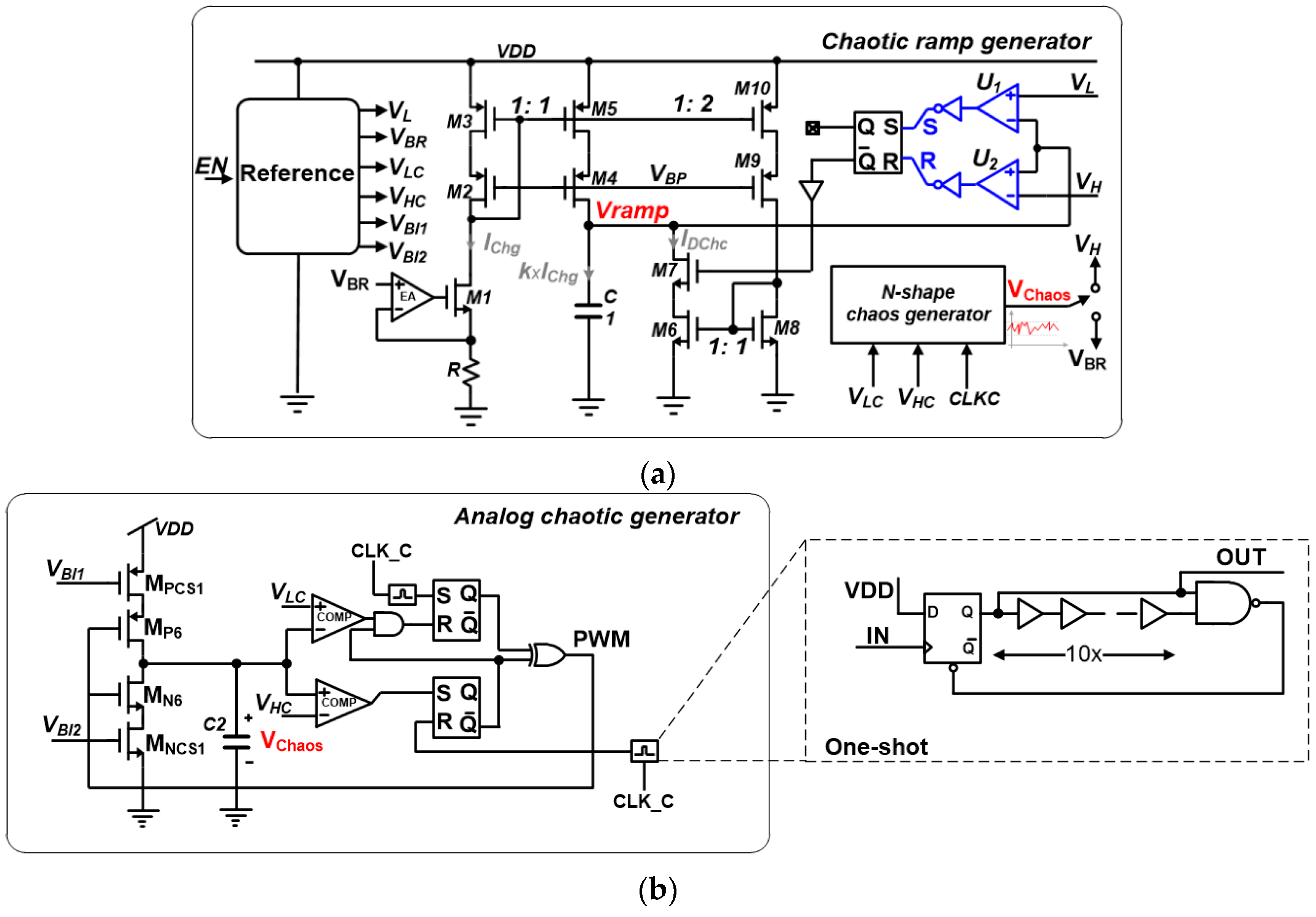
2. Proposed Chaos-Based EMI Reduction with On-Chip Chaotic Ramp Generator

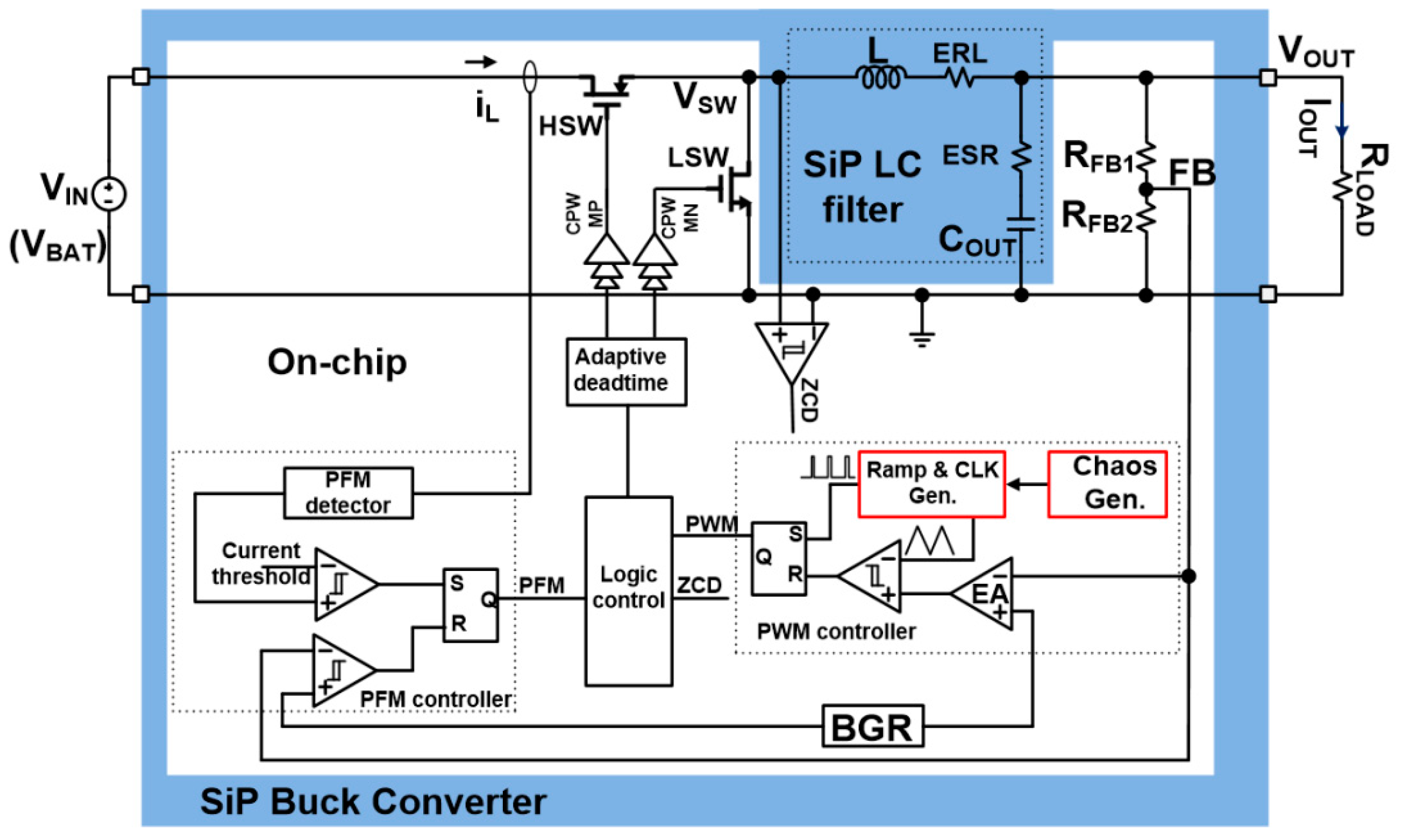
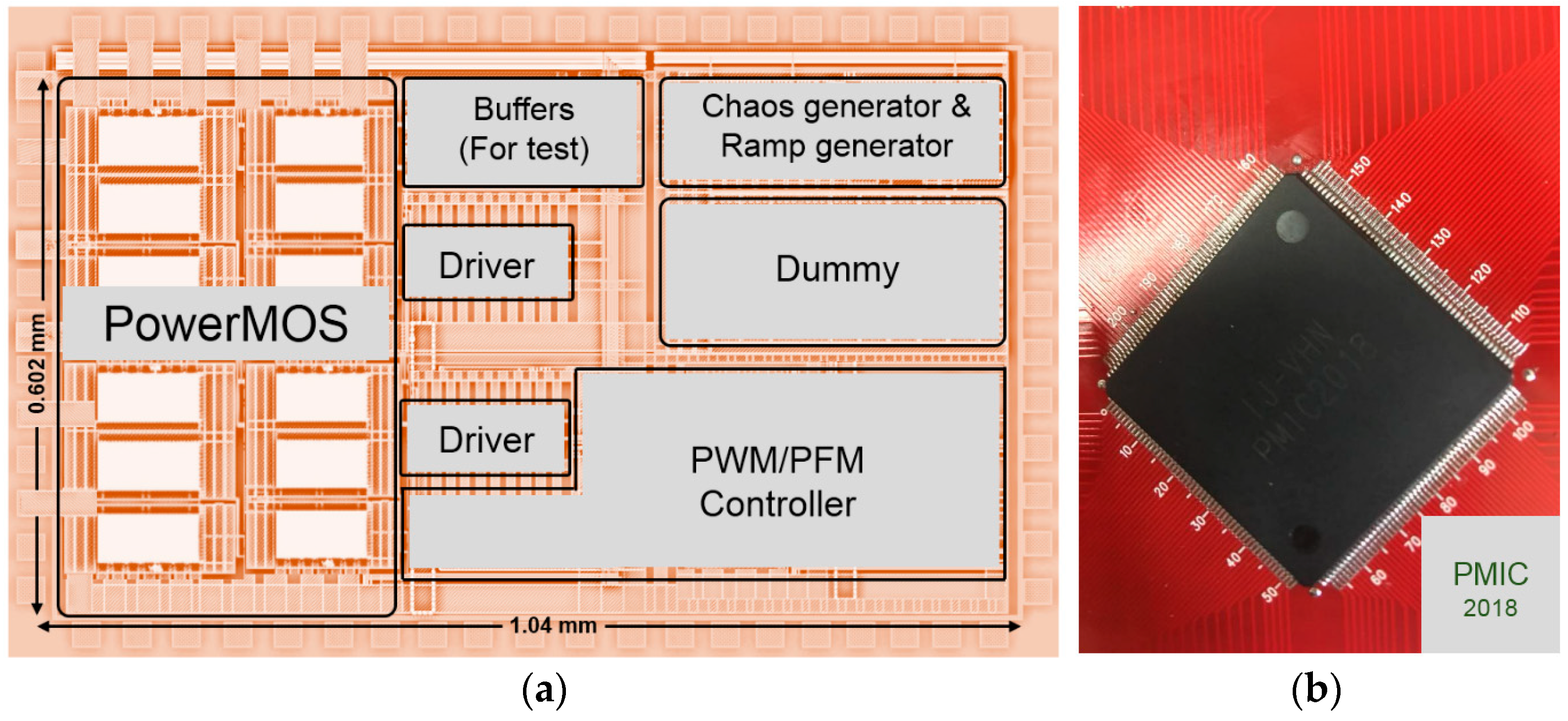
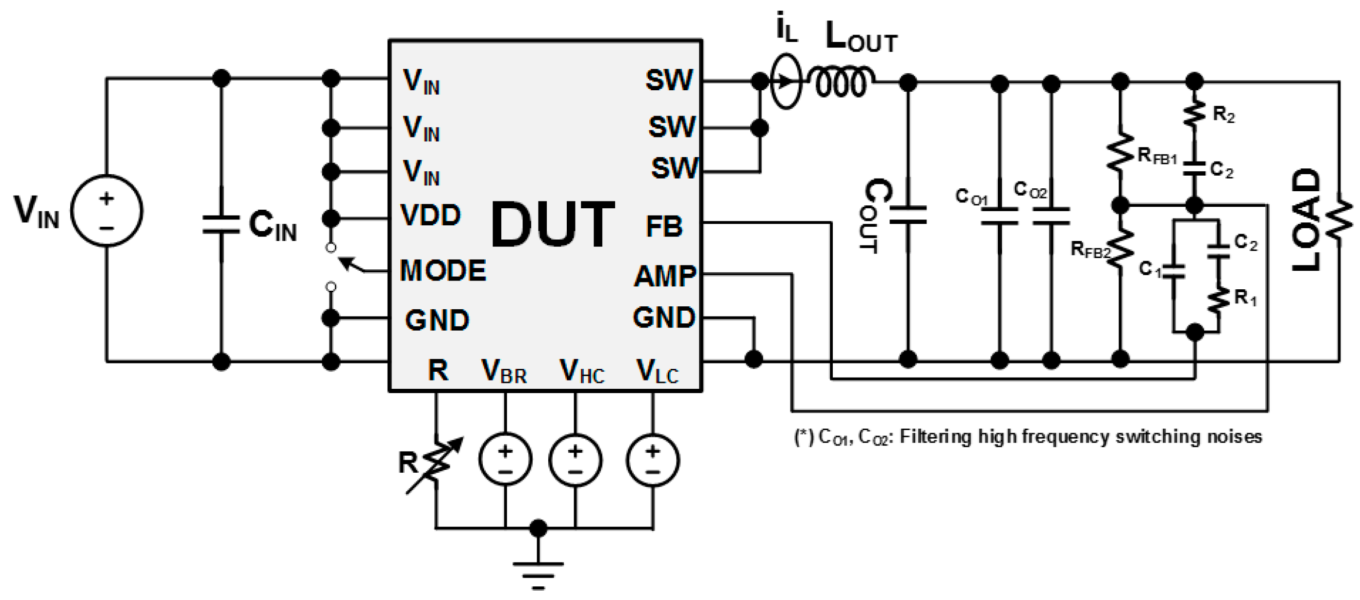
2.1. SiP Dual-Mode PWM/PFM Buck Converter with Chaos-Based EMI Reduction Scheme

Buck converters are indispensable in most battery-powered devices due to their simple power conversion step and high power efficiency. To maintain high power efficiency over a wide range of load currents, dual-mode PWM/PFM buck converters are widely used [19,20]. Figure 1 shows a simplified schematic diagram of our EMI-improved buck converter, along with the concept for a SiP buck converter powered by a battery represented by a voltage source (VBAT). The buck converter is controlled by a PWM/PFM controller to turn ON/OFF the high-side and low-side switches (HSW/LSW) with non-overlapping pulses CPWMP/CPWMN. To eliminate the conduction loss when the converter enters low load conditions, a comparator is utilized to output a zero-current detection (ZCD) signal to turn off the LSW by comparing the switching node voltage (VSW) and the ground. The bandgap reference (BGR) circuit outputs a reference level of 1.2 V to regulate the output voltage of the converter. Also, in the block diagram, (EA) represents the error amplifier, and equivalent series resistance (ESR) and direct current resistance (DCR) represent the parasitic resistances inside the inductor and capacitor of the LC filter, respectively. This work presents a DC-DC buck converter that features an automatic mode change between PWM and PFM depending on the load current level. The corresponding output to load is in the range from 50 mA to 500 mA. When the load current is higher than 200 mA, the converter operates in PWM mode. When the load current is lower than 200 mA, the converter automatically switches into PFM mode, in which the power stage operates intermittently, based on the load demand. In PFM mode, the switching activity is reduced to minimize the switching loss and maintain the high power efficiency of the converter.
Figure 2 shows the proposed scheme for generating a chaotic PWM signal for EMI reduction in a type-III compensation network. Type-III compensation is normally used for its optimized loop bandwidth and fast transient response in a voltage-mode-controlled converter that operates in continuous conduction mode (CCM) mode, as compared to type-I and type-II counterparts [21]. In this scheme, a fully on-chip N-shaped chaos generator circuit is proposed. Additionally, a new design for a symmetrically triangular ramp generator is implemented. The chaotic output of the N-shaped chaos generator (VChaos) is applied to control the triangular ramp generator (to VH or VBR) and generate a chaotic triangular signal (VCTR). The VCTR signal is then compared with the slow-varying signal at the output (VEA) of the error amplifier to generate the CPWM to control the high side switch (HSW) and low side switch (LSW) power switches. In chaotic operation mode, the switching period, TSW, varies chaotically, and the duty cycle also changes from cycle to cycle. However, the average duty cycle is constant, which means the output voltage follows the pre-determined value as expected. The inductor current and output voltage are also chaotic, so their associated spectra can spread over a certain frequency range. In this way, the EMI is significantly reduced using the characteristics of the broadband frequency spectrum in the chaotic signal. Most importantly, the scheme proposed here modulates the switching frequency (FSW) continuously in a defined range. This is equivalent to hopping among an infinite set of switching frequencies, which results in the full elimination of the peaks in the power spectrum present in the standard fixed-frequency PWM mode. Therefore, EMI reduction can be higher than that offered by previous solutions [17,18].
As described in the previous sections, EMI reduction via the spread-spectrum technique is always achieved at the cost of a performance reduction in the buck converter, including: (1) an increase in the output voltage ripple; (2) a increase in inductor current ripple; and (3) a reduction in power efficiency. However, those negative side-effects have often been neglected in the literature [16,17,18]. All of those factors require an increase in the size of passive LC output filter [8,22]. However, in the design of SiP buck converters, a large LC is not recommended, because the space inside the package is limited. This work mitigates those negative side-effects of the spread-spectrum technique by using a ramp generator to generate a triangular signal instead of a sawtooth. The triangular signal mitigates the ripple of the inductor current, thereby relaxing the requirement for large LC output filter. The overall specifications of our DC-DC converter are listed in Table 1. The details of the implementation of the proposed scheme are explained and discussed in Section 2.2 and Section 2.3 below.

2.2. Fully Integrated On-Chip Chaos Generator with N-Shaped Map

Chaotic sources have previously been proposed as a cheap replacement for a random signal in the spread-spectrum technique [23]. The chaotic signal plays a key role in the distribution of harmonics when a converter operates in the chaotic mode. So far, several CMOS chaos generators have been reported [23,24,25]. Those circuits, however, are not completely straightforward to design due to their lack of governing models [23], non-robust chaos with regard to variable circuit parameters [24], bulk, low frequency, and high power requirements [25].
In this section, a new, fully integrated on-chip, CMOS chaos generator is presented with its associated mathematical chaos map. The chaos map model can be strictly derived from the circuit operation, thus making the analysis and design simple and accurate. Because the chaos exists in a wide continuous range, the chaos robustness with respect to the unavoidable error introduced by physical variations in circuit devices can be significantly relaxed. Also, the compact design and low power consumption of the proposed chaos generator make it a good pseudo-random source. To achieve EMI reduction in the DC-DC buck converter, the output of the N-shaped chaos generator is injected into a triangular ramp generator to construct a chaotic ramp generator as explained in detail in Section 2.3.

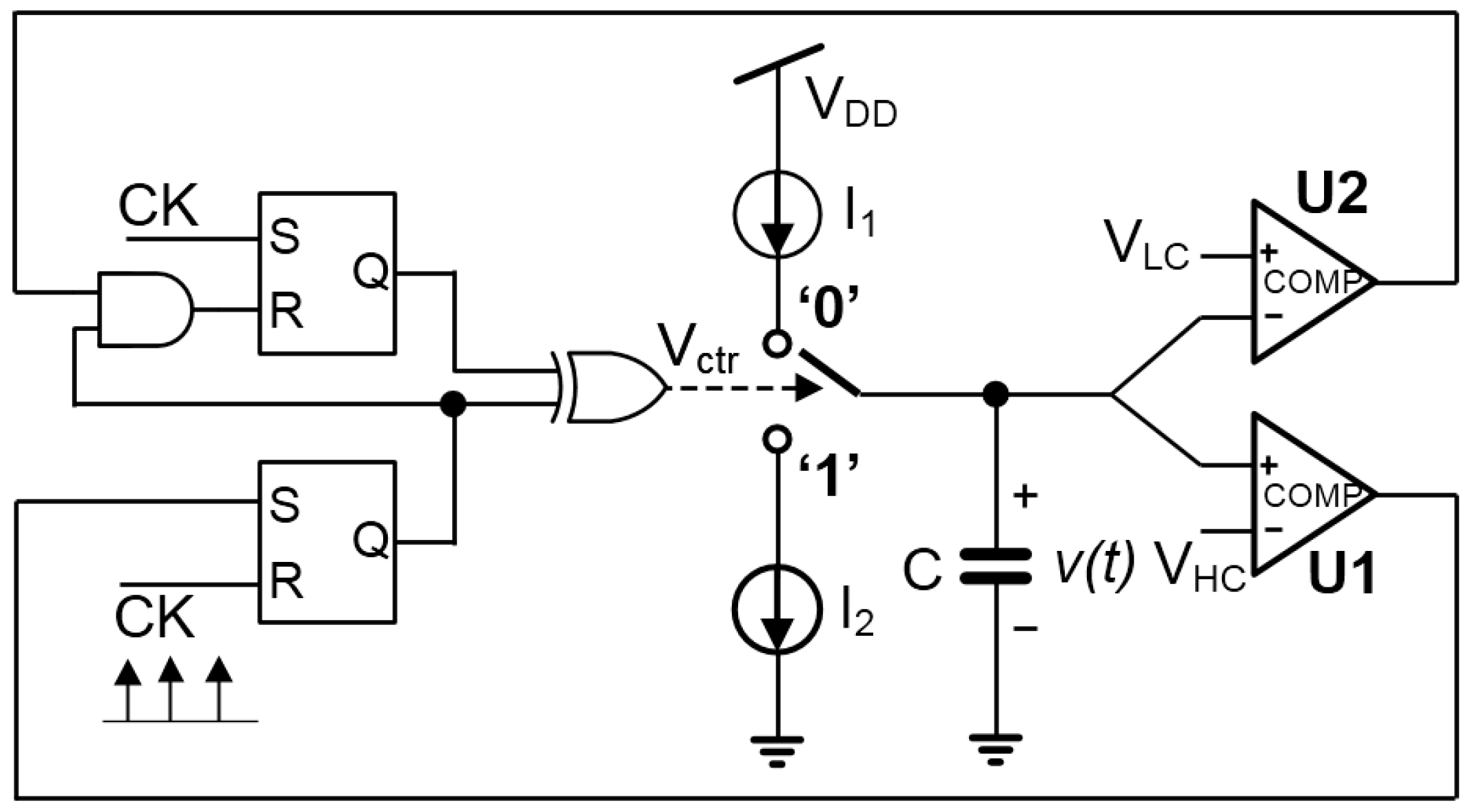
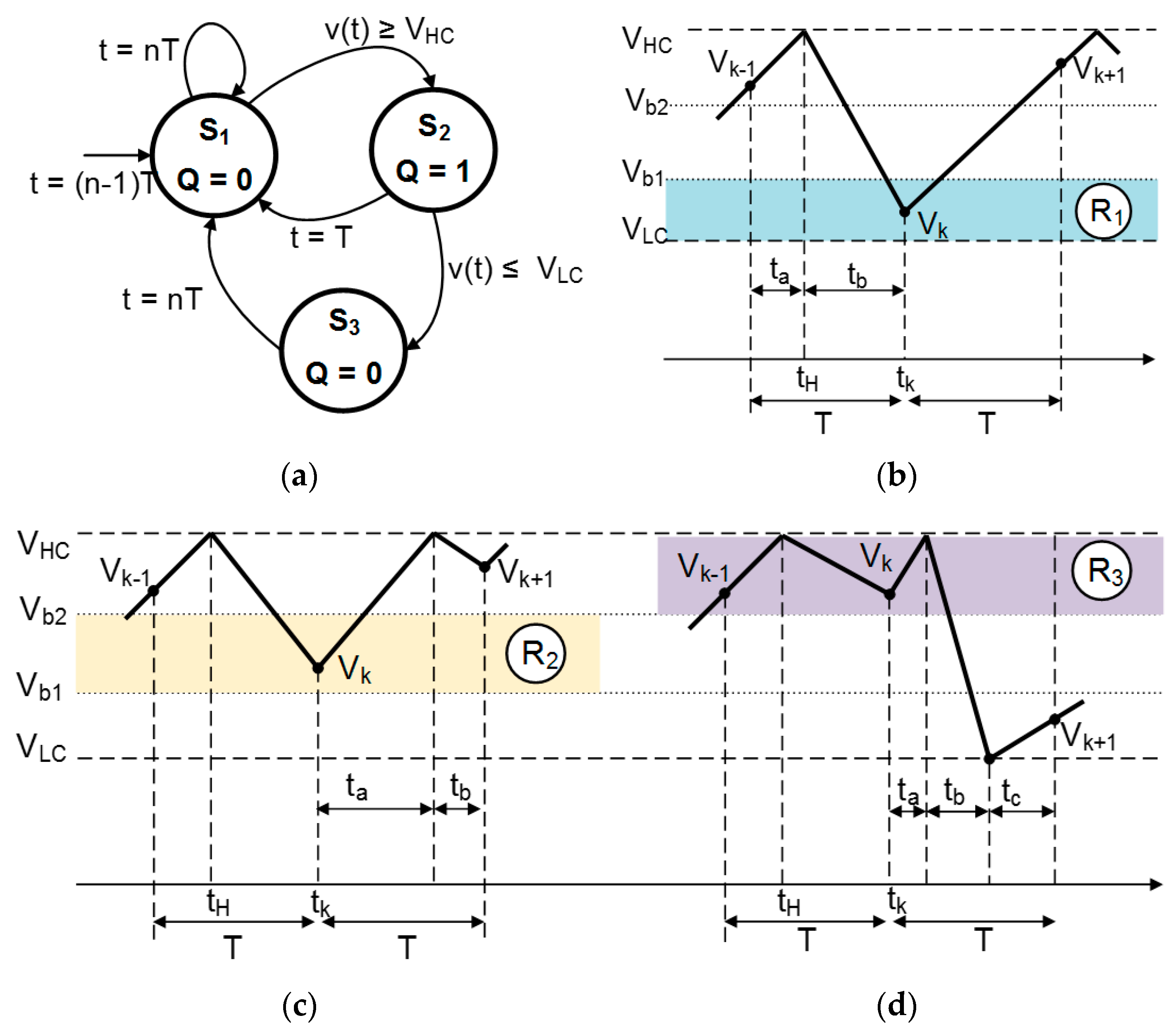
2.2.1. N-Shaped Chaos Generator

For the simplicity of the analysis, the proposed N-shaped chaos generator (CG) is simplified and shown in Figure 3. The circuit consists of one capacitor C that is either charged or discharged through two current sources/sinks (I1 and I2), respectively; the remaining part contains a controller with two comparators, two SR latches, one AND gate, one XOR gate, and one SPDT (single pole double through) switch. In the proposed chaos generator, the only state variable is the capacitor voltage v(t).
The operation of the chaos generator can be represented by a finite state machine (FSM), as shown in Figure 4a. The state machines S1 and S3 correspond to the charging of capacitor C at every rising edge of the clock (CK) or when v(t) reaches the upper limit VHC; the state S2 corresponds to its discharging when v(t) reaches the low limit (VLC). The dynamics of the proposed chaotic circuit can be represented by a 1-D piece-wise map, a so-called stroboscopic map. Assuming that at tH, the capacitor voltage reaches VH, which triggers the control signal Vctrl to be HIGH (Q = 1), capacitor C is discharged through I2 as follows:
v ( t ) = V HC I 2 C ( t t H )
Also, at the beginning of the next period (tk), Vctr is triggered to be LOW (Q = 0) by the clock signal, and capacitor C is charged by I1:
v ( t ) = V k + I 1 C ( t t k )
The 3 possibilities that the FSM can evolve depend on the value of state variable v(t) at tk. First, the state space is separated into 2 sub-spaces (R1 and R2 + R3), depending on boundary condition Vb1, which is defined as the voltage level at which the capacitor voltage is charged from VLC to Vb1 within one clock cycle T. Vb1 is calculated from discharging Equation (2) as follows:
V HC = V b 1 + I 1 C T V b 1 = V HC I 1 C T   ( V b 1 < V HC )
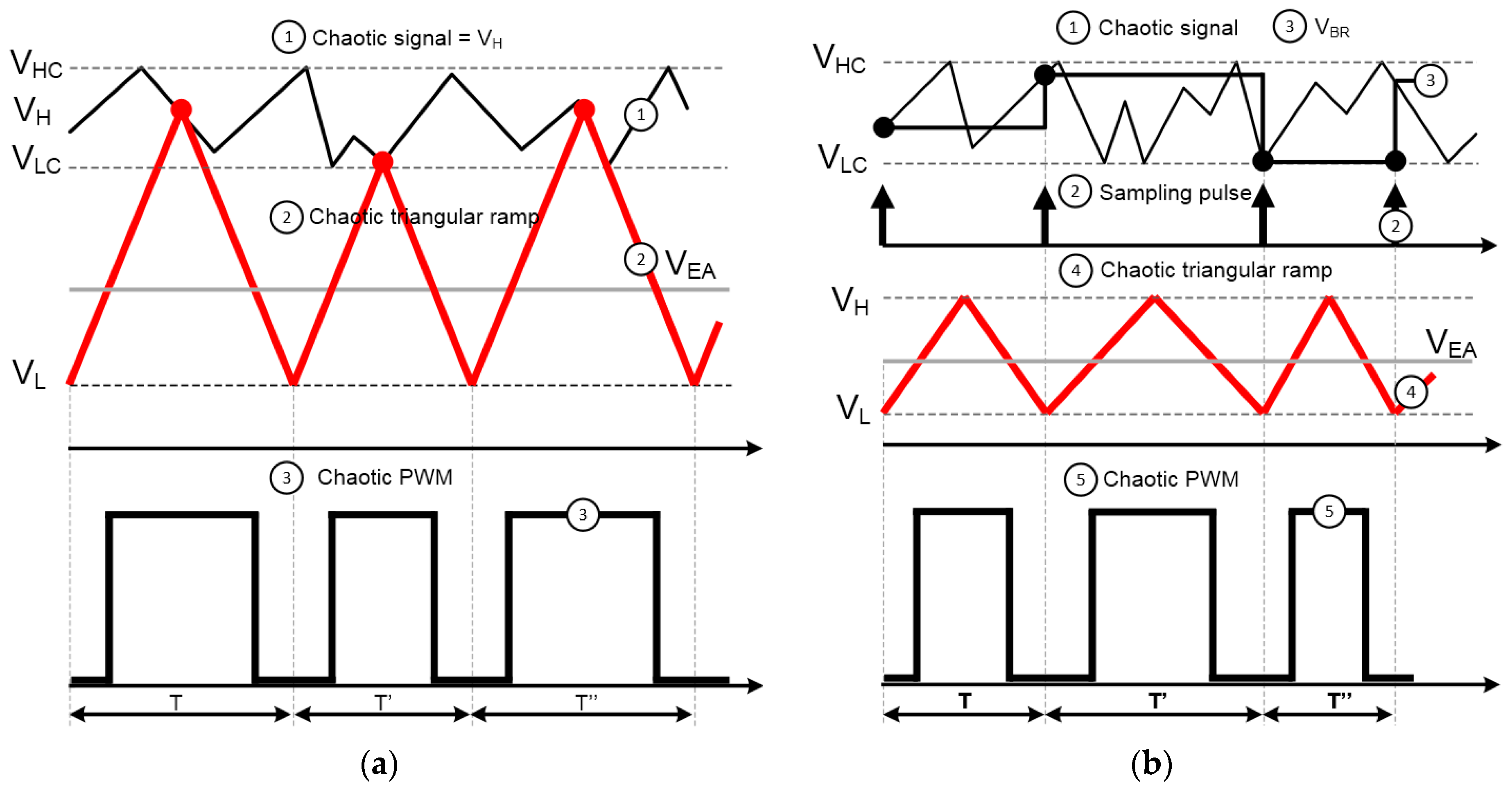
  • Sub space R1: At tk, if Vk < Vb1, the capacitor will continue charging on the next clock cycle as shown in Figure 4b, corresponding to FSM S1. However, if Vk > Vb1, the subspace higher than Vb1 can be divided into 2 other sub spaces, R2 and R3, depending on a second boundary condition, Vb2.
  • Sub space R2: The capacitor continues charging until v(t) reaches VHC and then discharge for the time durations ta and tb, respectively. Figure 4c shows the representative waveform for this case with the charging period ta and discharging period tb, which can be deduced from Equations (1) and (2): ta = I1/C × (VHC − Vk); tb = T − ta =T −I1/C × (VHC − Vk). For this case, ta + tb = T.
  • Sub space R3: The capacitor continues charging until v(t) reaches VHC, then it discharges to VLC for the periods ta, tb, and tc, as shown in Figure 4d. In this case, ta + tb < T; therefore, tc can be calculated as tc = T − ta − tb = T − I1/C × (VHC − Vk) − C/I2 (VHC − VLC). In this case, tb is different from before and can be calculated using the discharging equation VLC = VHC − I2/C × tb. The second boundary condition can be derived by the setup tc = 0:
    t c 0 T t a t b = T I 1 C ( V HC V k ) C I 2 ( V HC V LC ) 0 V b 2 = V HC I 1 C T + I 1 I 2 ( V HC V LC )
Now, the N-shaped map of the chaos generator that relates the value of state variable v(t) at every clock instant can be written as follows:
V k + 1 = { V k + I 1 C T ,   with   V LC < V k V b V HC I 2 C T + I 1 C ( V HC V k ) ,   with   V b 1 < V k V b 2 V k + T I 1 C ( V HC V LC ) ( 1 + I 1 I 2 ) ,   with   V b 2 < V k < V HC
Furthermore, that N-shaped map can also be normalized and parametrized:
x k = V k V HC ;   T 1 = T I 1 V HC × C ;   T 2 = T I 2 V HC × C ; x b 1 = V b 1 V HC ; x b 1 = V b 2 V HC ;
Thus, the normalized chaos map of the proposed chaos generator can be presented as:
x k + 1 = f ( T 1 , T 2 ; x k ) = { x k + T 1   with   0 < x k < x b 1 ; 1 T 2 + T 2 T 1 ( 1 x k )   with   x b 1 < x k < x b 2 ; x k + T 1 ( 1 V L C V H C ) ( 1 + T 2 T 1 ) ;   with   x b 2 < x k < 1 ;

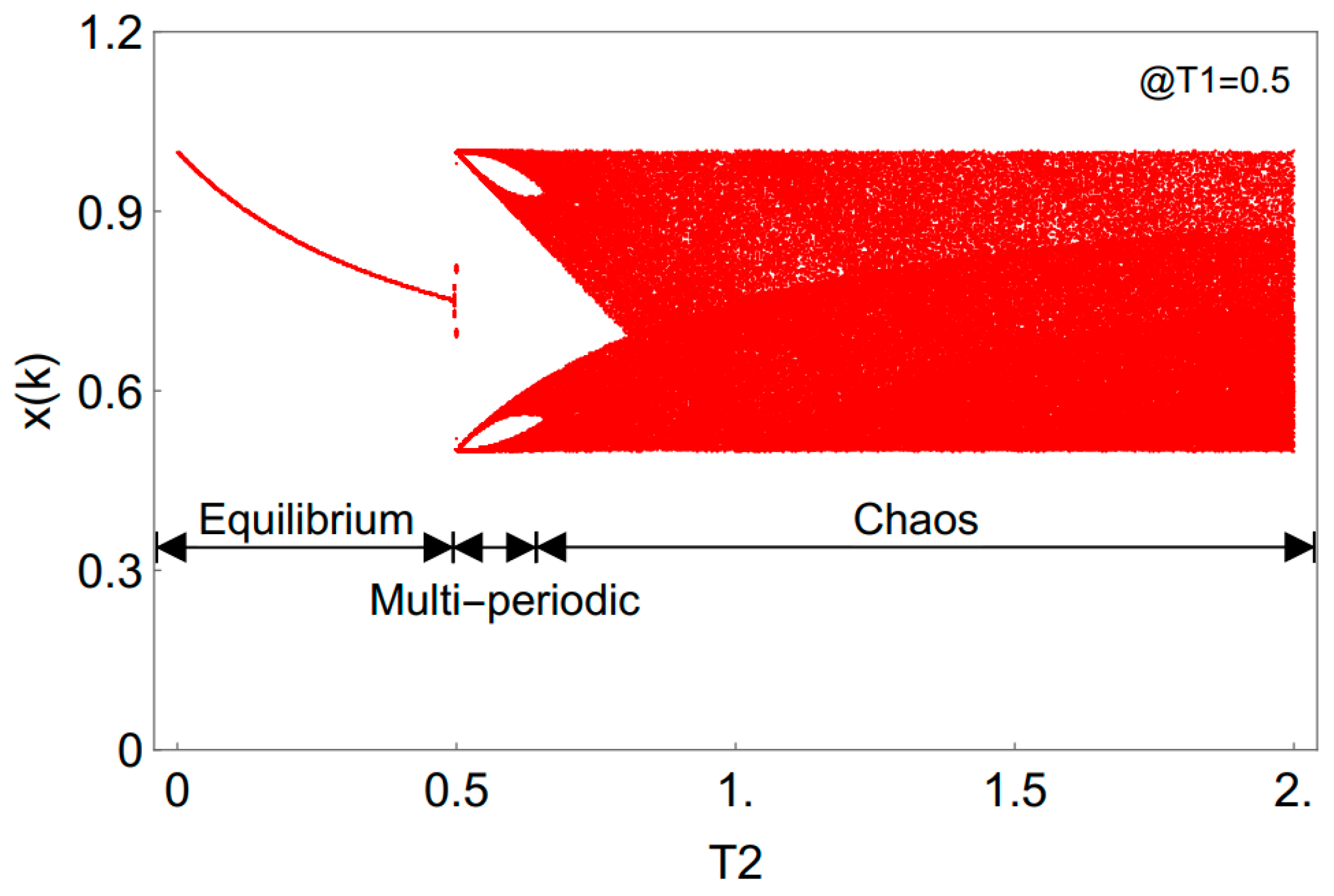
2.2.2. Dynamical Analysis of the Chaos Map

Before implementing the chaos generator at the circuit level, the proposed mathematical model for the chaos generator is realized to find the range of system parameters at which the circuit outputs chaotic signal. The dynamic behavior of a chaotic system can be qualitatively studied through Lyapunov exponents. The Lyapunov exponent of the N-shaped map is theoretically calculated as follows [26]:
λ = lim n 1 n j = 1 n ln | f ( x j ) |
where f’(.) is the derivative of the chaotic map f(.) and can be derived as:
f ( x ) = { 1   with   0 < x k < x b 1 ; T 2 T 1   with   x b 1 < x k < x b 2 ; 1 ;   with   with   x b 2 < x k < 1 ;
Hence, the Lyapunov exponent is calculated as follows:
λ = lim n 1 n ( i × ln 1 + j × ln | T 2 T 1 | + k × ln 1 ) = lim n j n ( ln | T 2 T 1 | ) ,   i + j + k = n
where n is the number of x points use in the calculation, i, j, k are the number of times that x belongs to three ranges [0, xb1], [xb1, xb2], and [xb2, 1], respectively.
According to Equation (7), when T2/T1 > 1 and λ > 0, the map produces periodic doubling bifurcation; in other words, a chaotic signal is generated [26]. Otherwise, if T2/T1 <1 and λ < 0, the system output has a periodic state or converges to a stable point. The chaotic dynamics can also be observed via the bifurcation diagram. For example, when T1 = 0.5 and T2 is gradually increased from zero, the bifurcation diagram appears as shown in Figure 5, from which the dynamic behaviors of the point, periodicity, and chaos (dense area) can be observed. The bifurcation diagram also highlights the robustness of the chaos generation from the map versus the system parameter (T2); there is no intermittent-periodic window inside the bifurcation diagram, unlike in previously reported work [16]. The circuit parameters for designing the N-shaped chaos generator in the next section can be selected easily based on the bifurcation diagram shown in Figure 5. The dynamics behaviors of the chaotic map can be further examined in another reported work [27].

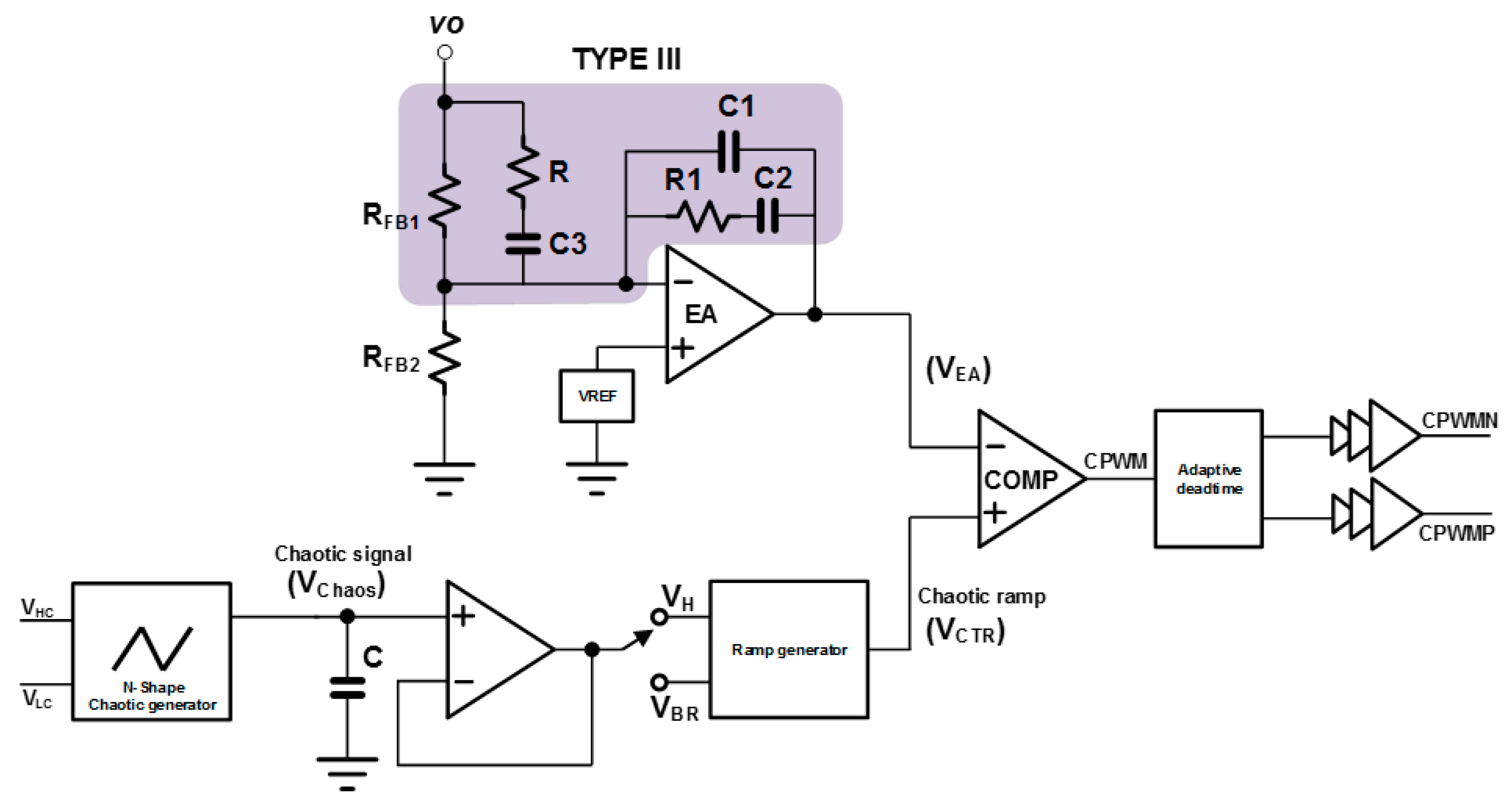
2.3. Design of Chaotic Triangular Ramp Generator

In the voltage mode of a DC-DC buck converter, a ramp signal is needed to modulate the PWM signal. Basically, there are two different possible forms for the ramp signal, a sawtooth ramp signal and a triangular ramp signal. The studies in [4] demonstrated that a symmetrically triangular ramp signal with equal rising and falling slopes can effectively mitigate the inductor current imbalance effect; therefore, it can also mitigate the aforementioned side-effects of the spread-spectrum technique without influencing the inductor current spectrum (and therefore the EMI performance). We therefore propose a PWM ramp generator that generates a triangular signal to reduce EMI and minimize the side-effects caused by the inductor current imbalance in the chaotic operation mode.
The detailed implementation of the proposed chaotic triangular ramp generator is shown in Figure 6a. The proposed chaotic triangular ramp generator consists of a triangular ramp generator linked with the proposed N-shaped chaotic circuit. Unlike a sawtooth ramp generator, in which the discharging time is much smaller than the charging time, the time for charging and discharging should be equal in a triangular ramp generator. Therefore, a current source/sink is used to control the charging/discharging speed to optimize the accuracy. This requirement preserves the memoryless property of the steady state inductor current, especially, when the switching frequency changes from cycle-to-cycle in chaotic operation mode. In the proposed triangular ramp generator shown in Figure 6a, the V-I converter (constructed from a error amplifier (EA), resistor (R), transistor (M1) and a wide-swing current source using cascade current mirror (M2–M5)) controls a charging current IChg = VBR/R. This current is copied by the current mirrors M6 and M8M10 to form a current sink that controls the discharging current IDChg. As mentioned before, the charging and discharging time for timing capacitor C1 must be equal, so IDChr = 2IChg. This is implemented by setting a current ratio between current mirrors M4–M5 and M9–M10 as 2:1. The operation of the proposed triangular ramp generator can be briefly described as follows: Assume that at the beginning, after an initial reset event (with the triangular signal at low threshold limit (VL)), the switch M7 is OFF and capacitor C1 is slowly charged with charge-current IChg until the capacitor voltage (ramp) reaches the upper limit (VH). At that point, the comparator trips, and the switch M7 switch is turned ON, which discharges the ramp to VL by the current sink M6 with IDChg = 2IChg. When the triangular signal ramps down to VL, another cycle begins [28]. To reduce the asymmetry of the triangular ramp signal caused by current mismatches in the current mirrors, the length of the transistors in the current mirror should be large.
Figure 6b shows the implementation of the proposed N-shaped chaos generator. In this circuit, the inverter MN6–MP6 plays the role of the SPDT switch, whereas the transistors MPCS1 and MNCS1 act as the current source I1 and current sink I2, respectively. The one-shot circuit is used to generate short pulses for the SR latches because the clock signal (CLK) ideally consists of an impulse train at the rate f = 1/T. Practically, these impulses are approximated by narrow pulses and implemented using the one-shot circuit. The N-shaped chaotic circuit parameter was designed based on the selection of the mathematical model’s parameters T1 and T2. For this work, T2 is selected inside the chaos region (as shown in Figure 5) for robust chaos generation against the variation inherent in process fabrication as mentioned in [27]. With the proposed N-shaped chaos generator, the output is chaotic, as long as T2/T1 > 1. This condition can be easily met, irrespective of the variation of capacitor C2 (usually up to 30% of the design value). Because T1 = T × I1/(VHC), T2 = T × I2/(VHC); therefore, setting the ratio T2/T1 > 1 is equivalent to setting the ratio I2/I1 > 1. This can be easily controlled at the circuit level using a basic current mirror and matching the layout between the current source/sink (MPCS1 and MNCS1).
The triangular ramp generator and N-shaped chaotic circuit are connected together to construct the chaotic ramp generator. The switching frequency of the triangular ramp generator proposed in Figure 7 can be expressed as [29]:
f S W = 1 T = I Chg 2 C ( V H V L )
where VH and VL are the high and low bounds of the triangular ramp signal, respectively. Clearly, Equation (7) shows that two parameters can define the switching frequency of the triangular ramp generator: the ramp bounds (VH and VL) and the charging current IChg of the triangular signal. To alter the switching frequency from cycle to cycle, one or both parameters can be modulated using the generated chaotic signal (Vchaos) from the N-shaped chaotic generator.
For the first scheme (peak modulation), keeping the low bound (VL) and the charging current (IChg) unchanged causes the switching frequency of the ramp generator to depend only on the high bound (VH). The chaotic signal generated from the N-shaped chaos generator can then be fed directly into the VH of the comparator, making VH = Vchaos; therefore, the switching frequency of the ramp generator is chaotically modulated. Figure 7a depicts the timing diagram for that method. For the second method (slope modulation), the chaotic signal generated from the N-shaped chaos generator can be indirectly fed into the V-I converter at VBR, making VBR = Vchaos. Its timing diagram is shown in Figure 7b. In this scheme, the chaotic signal is converted into chaotic charging/discharging currents; therefore, the ramp signal and switching frequency are also chaotic. The chaotic signal from the N-shaped ramp generator cannot be fed directly into VBR because that continuous chaotic signal also changes the charge/discharging current within one cycle. Therefore, the chaotic signal is sampled only at the end of each cycle by an impulse (S) signal from the low-threshold comparator (U1) inside the ramp generator circuit. This configuration keeps the charging/discharging current (IChg/IDChg) unchanged until the end of the current cycle and eliminates disturbances on the triangular waveform. The switching frequency deviation (ΔFSW) in the chaotic mode is set near the fixed-frequency mode at 1.2 MHz and the frequency envelope of the chaotic triangular ramp signal is in the range of:
( f S W L ; f S W H ) = ( I Chg 2 C ( V Hmax V L ) ; I Chg 2 C ( V Hmin V ) ) = ( I Chg 2 C ( V HC V L ) ; I Chg 2 C ( V LC V L ) )
for the peak modulation and:
( f S W L ; f S W H ) = ( I Chg ( min ) 2 C ( V H V L ) ; I Chg ( max ) 2 C ( V H V L ) ) = ( V LC R 2 C ( V H V L ) ; V HC R 2 C ( V H V L ) )
for the slope modulation. By using Equations (12) and (13), the circuit parameters of the chaotic ramp generator such as C1, IChg, VH, VL, VHC, and VLC can be derived for implementation. The derived values of VHC, VLC from Equations (12) and (13) in combination with the normalized and parametrized Equation (6) presented in Section 2.2 can then be used to calculate the circuit parameters for N-shape chaos generators T, I1, I2 and C. It should be noted that the N-shaped chaos generator confines its chaotic signal at the output within a defined band [VLC; VHC] by two comparators. This assures that the frequency deviation of the chaotic ramp signal can be accurately controlled. This characteristic adds extra controllability to the chaotic ramp generator as the frequency deviation can be customized.
Of the two methods for generating the chaotic triangular ramp signal presented above, the peak level injection offers easier implementation. The slope modulation is more complex because it samples the chaotic signal and thus needs an additional sampling circuit. The slope modulation scheme also requires a high bandwidth V-I converter because the speed for converting the chaotic signal into chaotic current needs to be fast enough for the charging current to switch from one level to another at the beginning of each cycle. In practice, the bandwidth of the V-I converter is set to at least 10 times the switching frequency. In designing the triangular circuit, because the ramp down slope of the triangle is lower than that of the sawtooth ramp generator, the design of the comparator is simple, and the power consumption of the comparator is low. Additionally, because the ramp amplitude directly affects the stability of the buck converter in voltage mode [21], the compensation network of the converter using a triangular ramp generator with peak modulation should be designed carefully. For the slope modulation method, the amplitude of the ramp signal is kept constant, and the stability does not change once the compensation network is fixed.

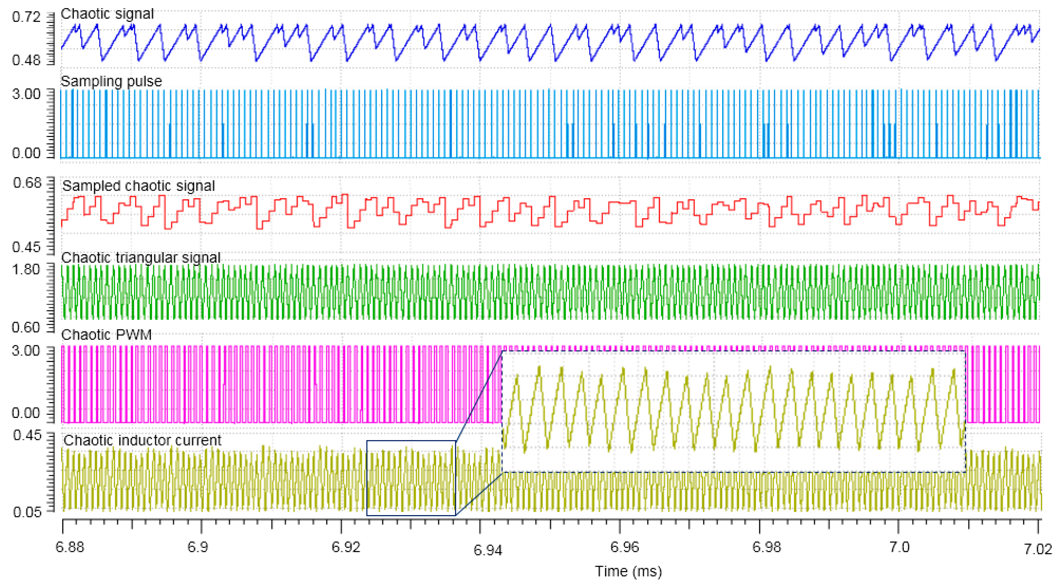
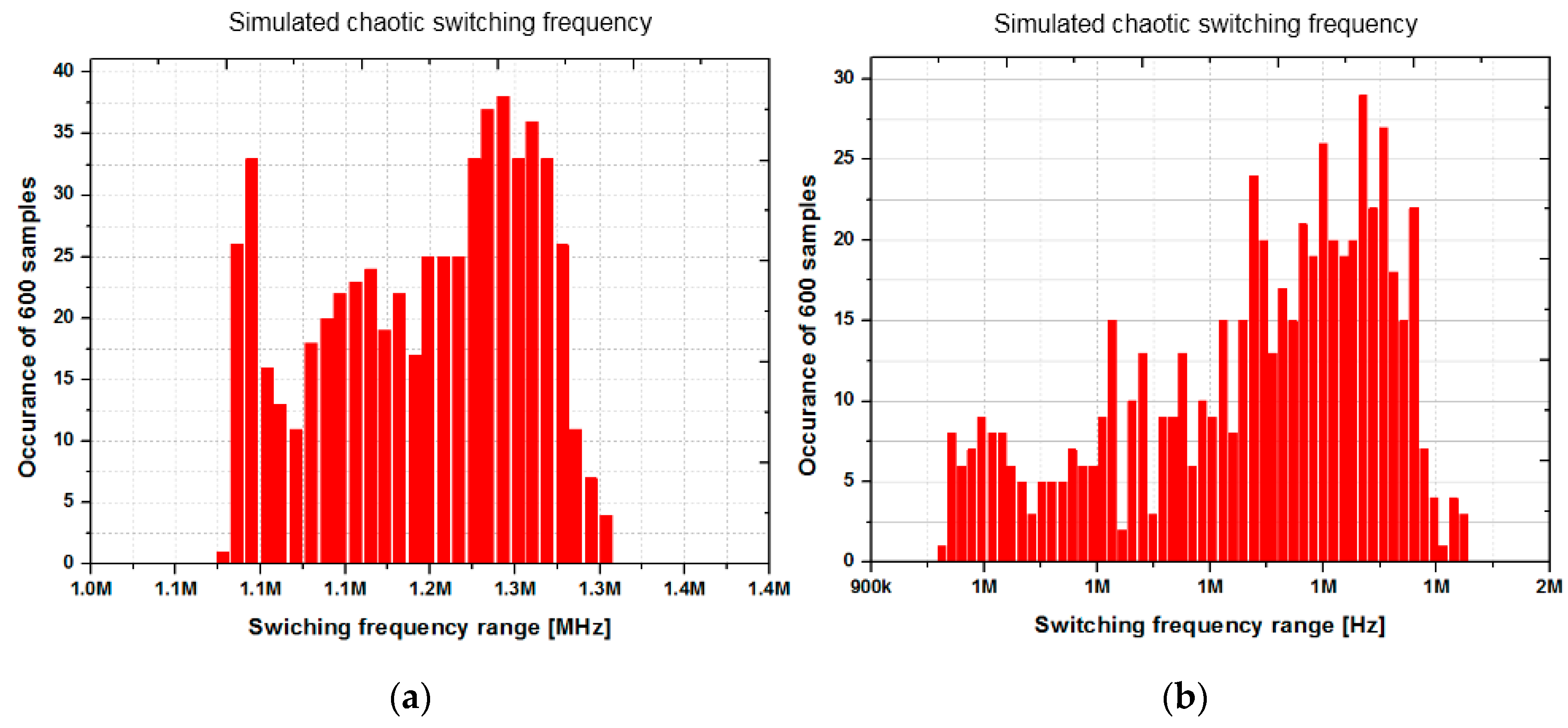
3. Simulation Results

Before fabricating a chip, we examined the performance of the proposed EMI-improved buck converter through a simulation. The chaotic ramp generator presented in the previous section was applied to the dual-mode PWM/PFM buck converter in Figure 1 to examine the EMI reduction performance. The simulation was conducted for both the standard mode and the chaotic mode for ease of comparison. The nominal switching frequency FSW for the standard mode was set to 1.2 MHz, and the chaotic frequency range was set at +/−10% of the Fsw (1.08 MHz to 1.32 MHz) and +/−20% of Fsw (0.96 MHz to 1.44 MHz).
In the standard mode, the design parameters of the triangular ramp were set at VBR = 0.6 V, C = 3 pF, VH = 1.5 V and VL = 0.8 V to achieve a nominal of FSW = 1.2 MHz. To achieve the frequency deviations of +/−10% and +/−20% around the nominal switching frequency FSW, the bounds of the chaotic signal (VChaos) applied to the VBR of the ramp were set at VHC = 0.66 V, VLC = 0.514 V, VHC = 0.71 V, and VLC = 0.46 V, in accordance with Equation (9). In the chaotic mode, the mean value of FSW = 1.2 MHz is defined using the mean value of VHC and VLC. Following the condition of T2/T1 > 1 or I2/I1 > 1 to output the chaotic signal, the parameters of the N-shaped chaotic circuit were set at: C = 3 pF, I1 = 1 μA, I2 = 6 μA, and CK = 1 MHz for both cases. The simulation setup for the converter was: VIN = 3 V, VOUT = 1.8 V, IOUT = 250 mA, L = 2.2 μH and COUT = 2.2 μF. The ESR value of the capacitor (ESR = 30 mΩ) and the other components of the compensation network were selected from commercial elements to give a good predictable result when comparing the simulation with the real test chip measurement results.
Figure 8 shows the simulation results for the converter when operating in the chaotic mode with the chaotic triangular ramp generator using slope modulation. Clearly, the chaotic signal from the N-shaped chaos generator is sampled at the beginning of each switching cycle and then fed into the V-I converter at the VBR of the triangular generator. As a consequence, the converter operates in the chaotic mode. The inset figure of inductor current shows that it varies chaotically; therefore, the EMI performance will be improved. The chaotic operation of the buck converter can also be easily confirmed from the phase portrait of two internal chaotic states (inductor current and output voltage) shown in Figure 9b. Compared to the standard mode shown in Figure 9a, in which the operation is stable between two equilibrium points and can thus be presented by only one trajectory, the chaotic operation shows a complex pattern, including multiple un-repeated trajectories that represent chaos.
The simulated switching frequency distribution of the chaotic triangular ramp generator using slope modulation is shown in Figure 10. To achieve the most flattened power spectrum, a uniformly distributed switching frequency is most desirable [18]. As seen in Figure 10, the distribution of the chaotic switching frequency is not uniformly distributed over the desired frequency range. However, the frequency spreads out continuously in the pre-defined range; therefore, harmonic peaks in the power spectrum in chaotic mode are expected to disappear.
Generally, the EMI reduction of the switched-mode dc-dc converters using spread spectrum technique can be verified by analyzing the power spectrum [16,17,18]. The power spectrum of the switching node and the output node were calculated using the available spectrum analyzer tool in Cadence software. Because of the intended target is to show the power spectrum up to 30 MHz, the resolution bandwidth (RBW) for the calculation of power spectrum was 6.67 kHz. The selected bandwidth for the spectrum analyzer in Cadence was also setup at 5 GHz for capturing all the harmonics for the analysis. Figure 11 and Figure 12 show the simulated power spectra of the output node and switching node under different conditions of frequency deviation under ILOAD = 250 mA. The spectrum of the converter in the standard mode with a fixed switching frequency of FSW = 1.2 MHz is included as a benchmark for comparison with the chaotic mode. Clearly, the power is densely concentrated at the fundamental frequency of 1.2 MHz and its harmonics when the converter operates in standard mode, whereas the spectrum is continuous and the amplitudes of the spectral peaks are reduced in chaotic operations. This is because the total emitted energy does not change; instead, the energy gets spread over a wider frequency range, thereby reducing peak emissions [30]. To determine the optimal frequency deviation in the chaotic mode in terms of EMI reduction performance and minimize the negative side-effects, the proposed design was simulated for 2 cases. For the first case, the switching frequency was chaotically varied within +/−10% of FSW, which reduced the fundamental harmonic peak from −13.34 dBm to −28.4 dBm at the output node and improved the peak at the switching node from 10.12 dBm to −4.87 dBm. The improvement of the power spectrum of the output node is similar to that of the switching node, and the EMI reduction for this case is approximately 15 dBm. For the second case, when the frequency deviation is increased to +/−20% of FSW, the EMI reduction is approximately 19 dBm.
As shown in the power spectra in Figure 11 and Figure 12, as the frequency deviation increases, the power spectra can be effectively spread over a wider frequency range, thereby reducing the peaks at the harmonic frequencies to much lower levels. In previous works using the randomized modulation technique [17,18], the power at the harmonic frequencies was spread out around discrete fixed-frequency levels. In particular, using the theory reported in [18], and assuming that randomness was assured, the theoretical reduction (ideal case) in the power spectrum using 2, 4, and 8 switching frequencies was 6 dB, 12 dB, and 18 dB, respectively. Using the spread-spectrum chaotic modulation proposed here, the reduction in the power spectrum can easily be more than 18 dB without the requirement of randomness because the power spectrum is spread continuously out rather than clustered around discrete frequency harmonics. Also, the hardware implementation of this proposed system is much simpler than that in the previous work. Therefore, the proposed design outperforms those earlier works.
Theoretically, the inductor current imbalance effect caused by the time-varying switching frequency in chaotic mode can be eliminated by using the triangular ramp generator. In fact, the non-idealities, such as the non-ideal triangular ramp and the delay in the drivers and controller, will cause a small imbalance in the inductor current; therefore, in fact, the low-frequency ripple caused by the chaotic switching frequency still exists [4,28]. This perturbation will be injected into the output voltage at the switching frequency. A feedback network in response to perturbation at such a high rate of change cannot occur in a voltage-mode converter with limited bandwidth (0.2–0.3 switching frequency (FSW)), so the perturbation from the inductor current imbalance is injected into the output node. THis increases the output voltage ripple compared to the fixed-frequency PWM operation mode. After a few cycles, the amount of output voltage ripple accumulates, and the feedback network will start to respond and remove the redundant voltage. Figure 13 shows the simulation results for the inductor current ripple and the output voltage ripple when the converter operates in chaotic mode. As seen in this figure, the converter output ripple increases compared to the standard fixed-frequency mode (and the mean value of the output voltage is considered to be unchanged). In particular, the output ripple is more than two-fold (28 mV vs. 13.36 mV of standard mode) with FWS +/− 10%, while the output ripple is more than three-fold that of standard mode when the switching frequency deviation ΔFSW is increased to +/− 20% (36 mV vs. 13.36 mV of standard mode). Clearly, the output voltage ripple in the chaotic PWM mode is much higher than in the standard fixed-frequency PWM mode.
As presented previously, there are two schemes for chaotic modulation in the triangular ramp generator: peak modulation and slope modulation. All of the simulated results above are based on the triangular ramp generator using slope modulation. To re-confirm the advantages of slope modulation, we also checked the performance of the converter with the ramp generator using peak modulation. Under the same frequency deviation condition with peak modulation, the output ripple rose to 213 mV and 549 mV, and the inductor current ripple rose to 549 mA and 984 mA, respectively, for 10% and 20% of switching frequency deviation. This confirms that peak modulation should not be used in the chaotic ramp generator even if the EMI performance could be improved significantly because of the large trade-offs in the output voltage ripple and inductor current ripple.
The results from the simulation showed that the frequency deviation (ΔFSW) should be small to limit the effects on the output ripple and the inductor current ripple, but it should also be large to achieve a significant EMI reduction. Therefore, the value of ΔFSW should be determined by balancing the trade-off between the ripple performance and the EMI of the converter. The switching frequency deviation should not usually be more than 20% because of the large trade-offs on the primary performance, such as output voltage ripple, inductor current ripple, and power efficiency. For example, when ΔFSW was higher than 20%, the output voltage ripple was increased by orders of up to 10 mV, which is unacceptable for practical use. Additionally, the high inductor current ripple with the triangular ramp using peak modulation adds difficulty in designing the PWM/PFM controller, because the load current is indirectly sensed through the inductor current when switching between the PWM/PFM modes. Because the inductor current ripple changes from cycle-to-cycle, unexpected ring switching will happen between PWM and PFM. Therefore, the triangular ramp generator using slope modulation is more appropriate because of it much lower ripple. Finally, it is important to understand that the effect of a fixed frequency of the clock (CK) in the chaotic circuit does not affect the EMI reduction performance of the proposed scheme, as was found in [18], because the operation of the converter is asynchronous with the clocking signal (CK) of the chaos generator. As shown by the power spectrum when the converter is in chaotic mode (Figure 11 and Figure 12), it does not peak at CK = 1.2 MHz.

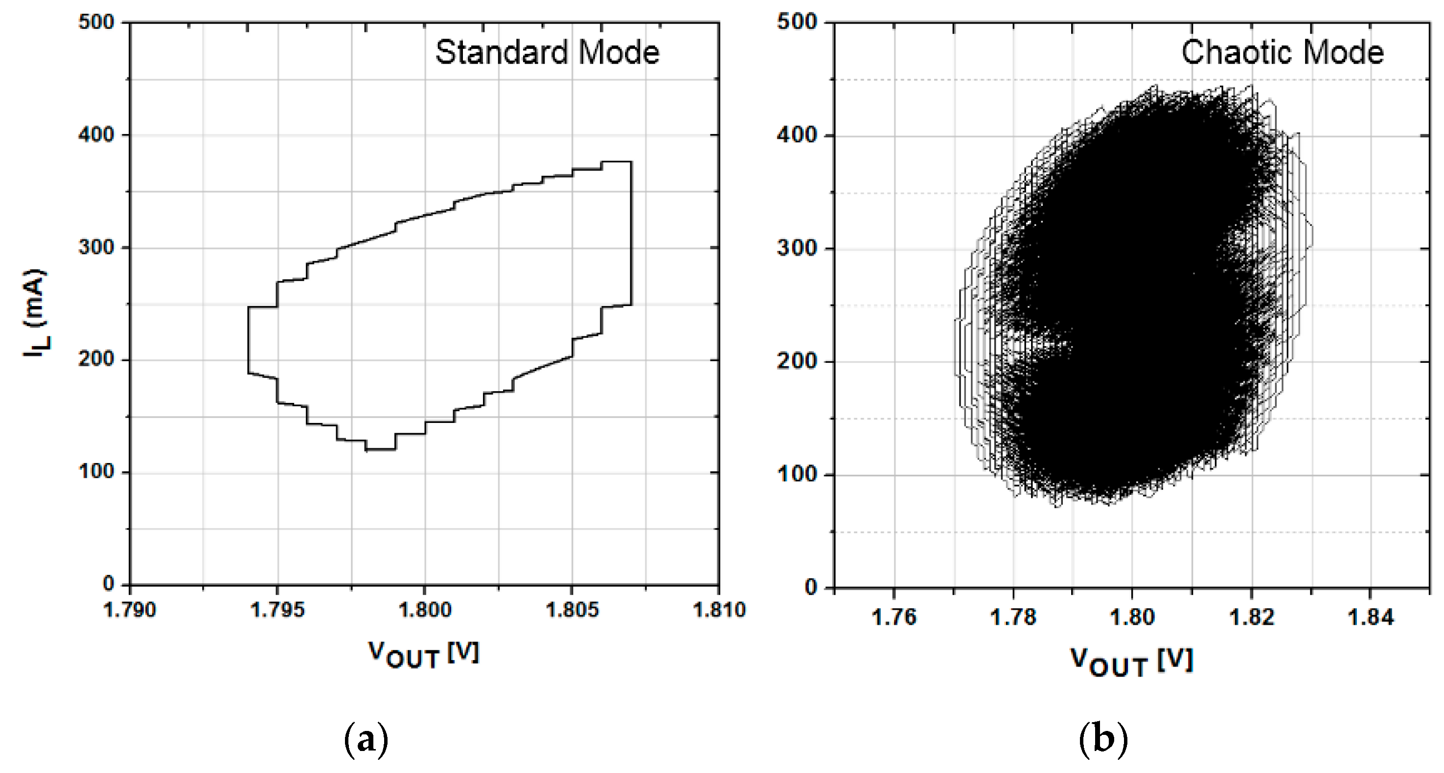
4. Experimental Results and Discussion

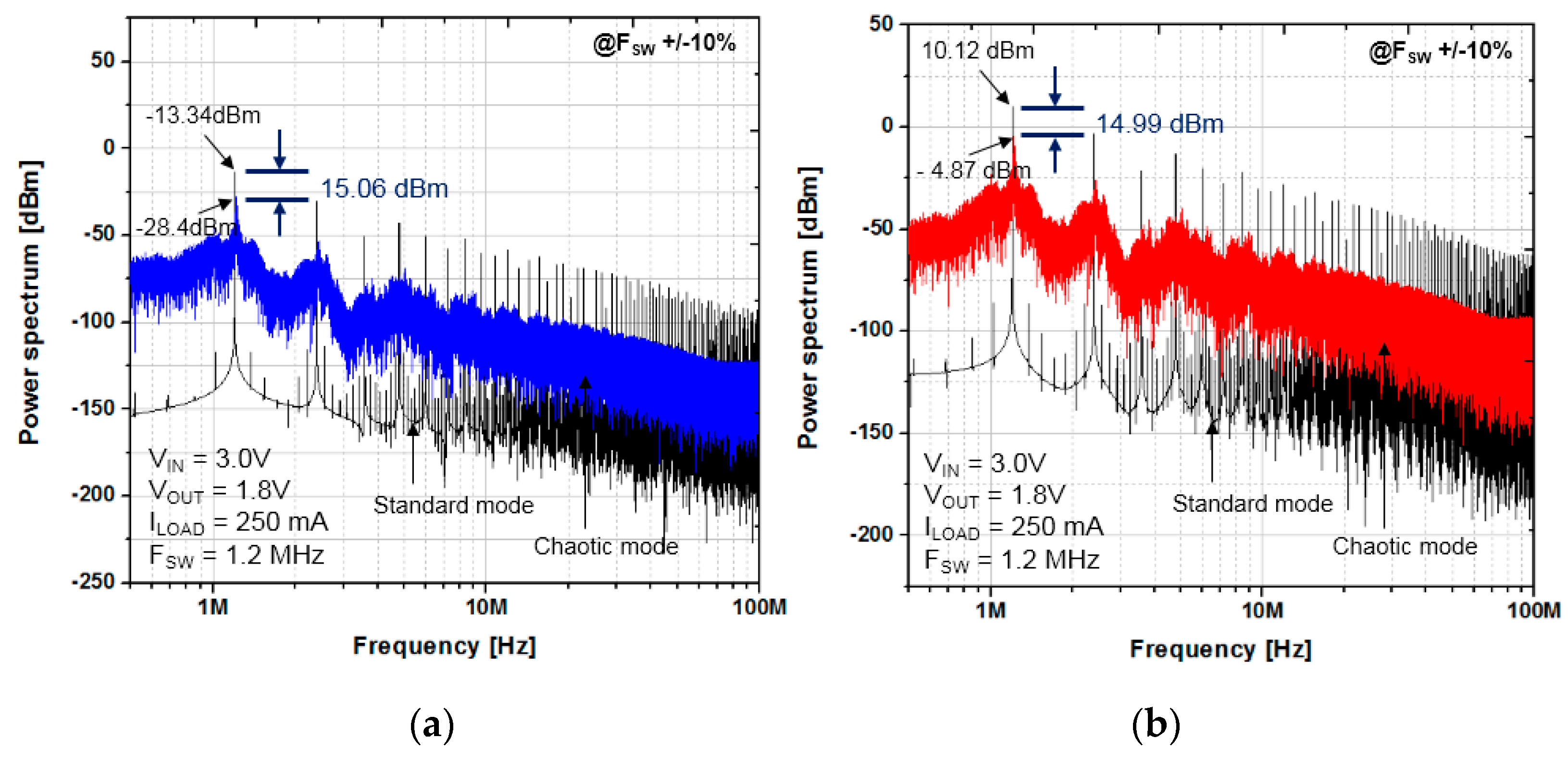
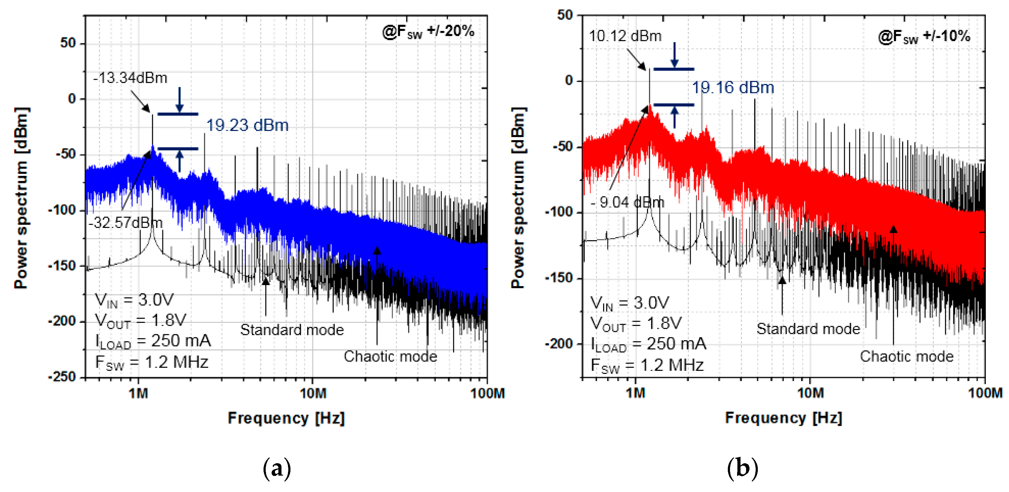
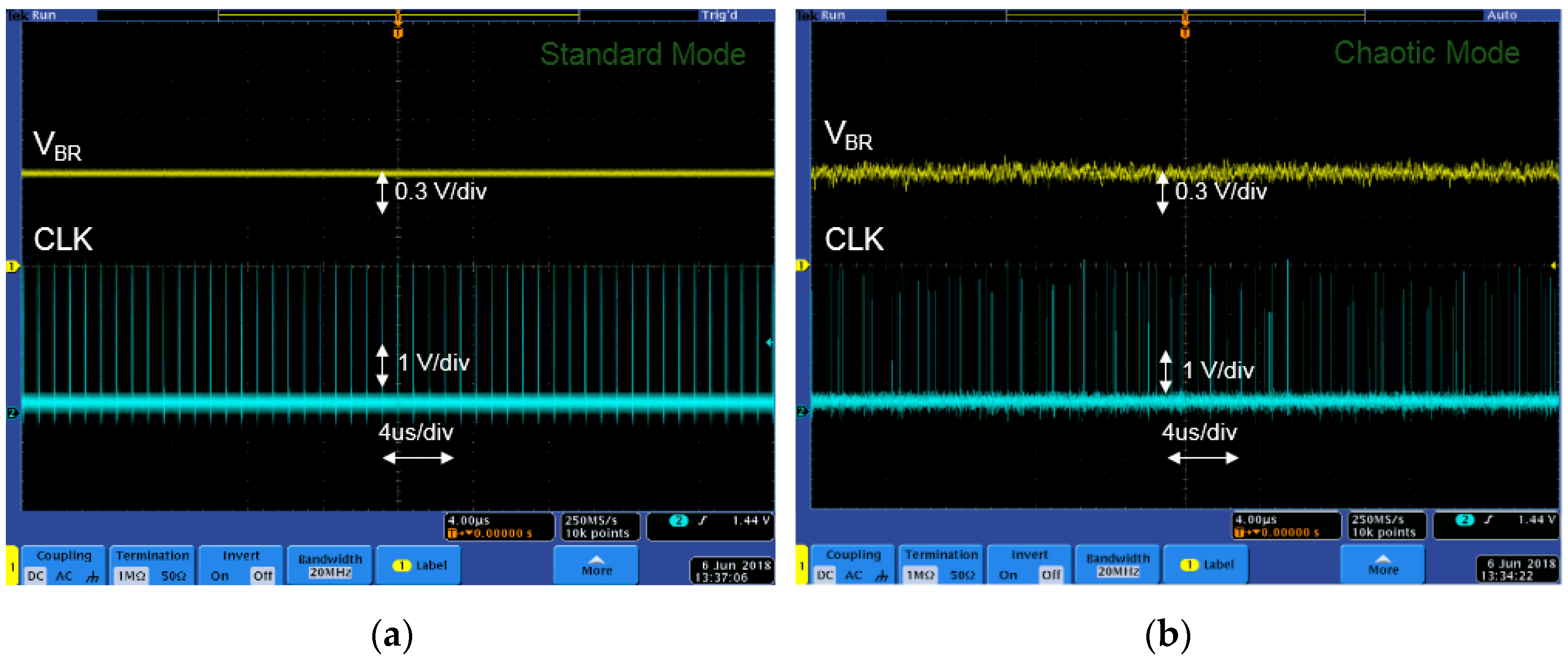
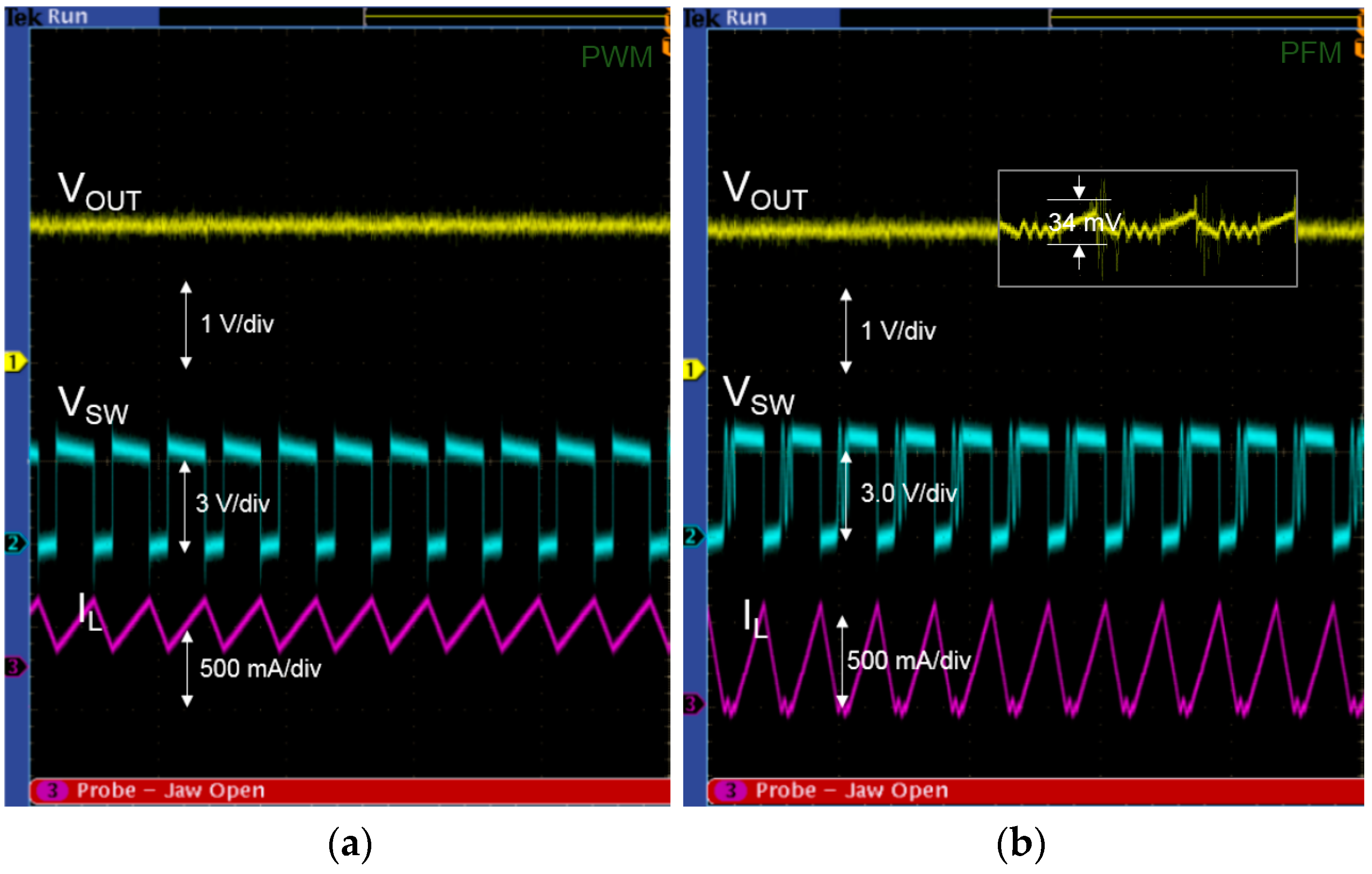
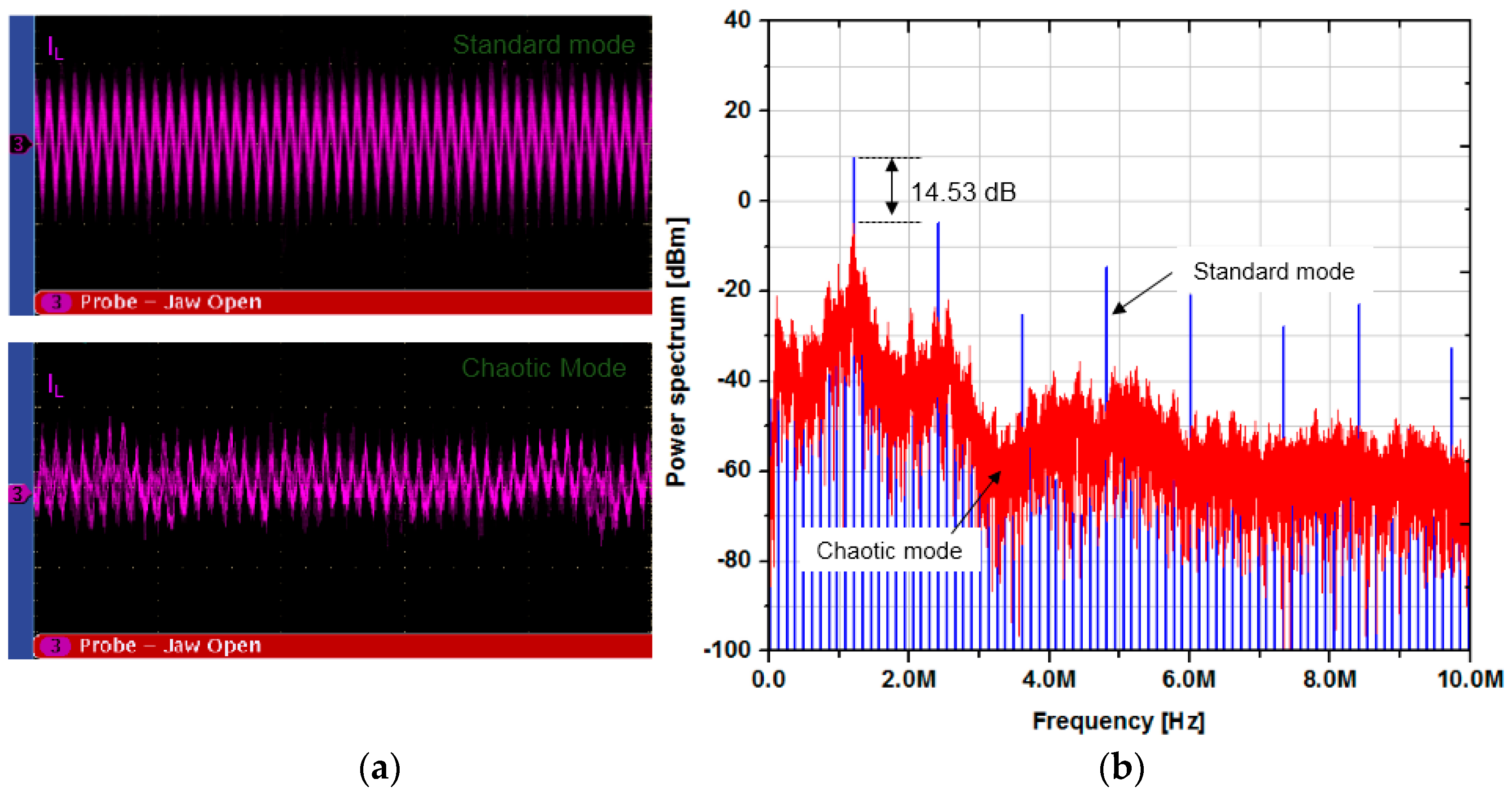
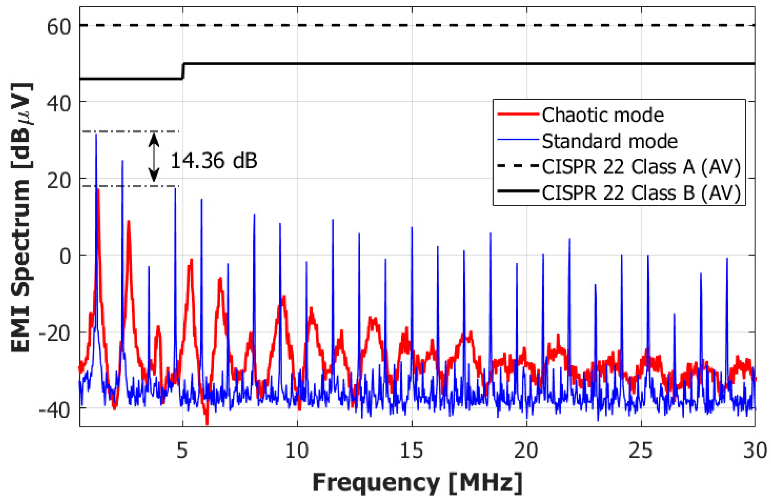
4.1. EMI Reduction Performance of the Proposed Scheme

To verify the proposed chaotic PWM scheme and compare it with a fixed-frequency PWM, a buck converter with the proposed chaotic ramp signal generator and slope modulation was designed and fabricated using a 3.3 V, 0.18 µm, CMOS one-poly six-metal-layers process. The active chip area was 0.626 mm2 (0.602 μm × 1.04 mm), excluding bonding pads, where the power transistors occupy 520 × 365 μm2. The chip photograph and the chip mounted on PCB for testing are shown in Figure 14. The experimental setup is shown in Figure 15 and the list of component values for the prototype is shown in Table 2. The terminal MODE (MODE = 0:Fixed-frequency PWM, MODE = 1:Chaotic PWM) can switch between the standard fixed-frequency PWM mode and the proposed chaotic PWM mode. Unless otherwise stated, all of the following results were measured using an input voltage of 3.3 V.
First, we constructed an experiment to examine the operation of the ramp generator to verify its functional operation before checking the EMI performance of the proposed scheme. Figure 16 shows the measurement results for the ramp generator in two modes (controlled by the MODE terminal). Because the parasitic capacitor on the voltage probe terminal of the measurement equipment is quite high (up to 10 pF) compared to the internal capacitor of the ramp and clock generator (2 pF in this study), the ramp signal should not be measured directly. Instead, an on-chip reading buffer was embedded to measure the clock signal inside the chip. The biasing current resistor (R) of the V-I converter for the triangular ramp generator is off-chip in order to tune the biasing current of the ramp generator in the prototype. When the MODE terminal is connected to the GND, the triangular ramp generator works in standard mode, whereas it works in chaotic mode when the MODE terminal is connected to the VDD. Figure 16a,b shows the measurement results from the triangular ramp generator for the standard mode and the chaotic mode (FSW +/− 20%), respectively. Clearly, the switching frequency is a constant for the standard mode when a fixed VBR is used and chaotic when chaotic VBR generated from the N-shaped chaos generator is used. The measured constant FSW is approximately 1.2 MHz (MODE = 0 V, VBR = 0.61 V), and the measured chaotic switching frequency is in the range from 1.06 MHz to 1.37 MHz (MODE = VDD; VBR is chaotic when internally connected to the N-shaped chaos generator; VHC = 0.73 V, VLC = 0.41 V (tuned values)). The experimental result for the triangular ramp generator matches well with the simulation result, with only a small mismatch caused by chip fabrication.
To test the EMI reduction in chaotic mode, the operation of the designed PWM/PFM buck converter in standard mode with a fixed switching frequency was also confirmed. Figure 17 shows the experimental results of the converter in standard mode under different load conditions (250 mA–PWM and 150 mA–PFM). The measured output ripples were 17 mV and 28 mA for the PWM and PFM modes, respectively.
Because the switching node (rather than the output) is the dominant source of EMI [18], we evaluated the EMI performance by looking at the peaks in the power density spectrum of the inductor current (IL), aiming to reduce it compared with its fixed-frequency counterpart. To evaluate the effectiveness of the proposed scheme, the inductor current of the buck converter in both the standard and chaotic mode was measured and analyzed using the discrete Fourier transform in MATLAB to estimate the EMI reduction. Figure 18a shows the measured inductor current in standard mode (top) and chaotic mode (bottom) with 10% switching frequency deviation, and Figure 18b shows their associated power spectrum analyses. The peaks that appear at the multiples of the fundamental frequency, FSW, are dramatically suppressed compared to the standard mode, similar to the simulation results in the previous section. The observed peak reduction at the first harmonic is about 14.53 dB, which agrees closely with the simulation result (15 dB). In fact, these differences come from the statistical properties of the chaotic output trajectory (in other words, the statistics of the chaotic frequency distribution). Also, the peak of the first harmonic of the power spectrum is at approximately 1.214 MHz for the standard mode, whereas the highest peak harmonic in the chaotic mode is at 1.2 MHz. Thus, the chaotic frequency distribution is focused at 1.2 MHz in chaotic mode, which slightly lowers the power spectrum reduction level of the proposed scheme. Additionally, the low spectrum peaks in the low-frequency range (lower than the minimum chaotic switching frequency) come from the low-frequency disturbance of the inductor current when the chaotic PWM is applied. However, it is still much lower than the other peaks, so it is not a concern related to EMI.
Comparisons with the standard are necessary to demonstrate the effectiveness of the proposed method. The EMI measurements of the buck converter in standard and chaotic modes are shown in Figure 19 along with the CISPR22 A-B limit. The EMI reduction obtained from the measurement is 14.36 dB at the fundamental switching frequency. The results show that operating the converter in chaotic mode reduces the EMI in the low-frequency range, which is consistent with the power spectrum analysis. The proposed method reduces the EMI of the DC-DC converter and satisfies the EMI standard is indicated in CISPR 22. In the test setup, the LISN (impedance stabilizer network) is located between the input power supply and the DC-DC converter under test [17]. Power spectrum analyzer is set at RBW = 3 kHz, and the frequency range of the measurements is 0.5–30 MHz.
The EMI performance of the proposed chaotic PWM scheme and other state-of-the-art works using the spread-spectrum technique are compared in Table 3. The proposed scheme achieved better EMI performance than the other alternatives compared. The performance of the proposed scheme can be explained by the fact that the chaotic switching frequency in the proposed scheme is continuously spread out within a certain frequency range rather than swept at several random fixed-frequency levels, as presented in [17,18]. In addition, the randomized PWM methods in [17,18] are usually costly because of their complex designs and the difficulty of confirming randomness. The most appealing advantage of the proposed scheme is that it can be easily embedded into any PWM buck converter using a standard ramp generator without modifying the overall structure. Therefore, the proposed scheme offers a cheap and effective solution for practical usage.

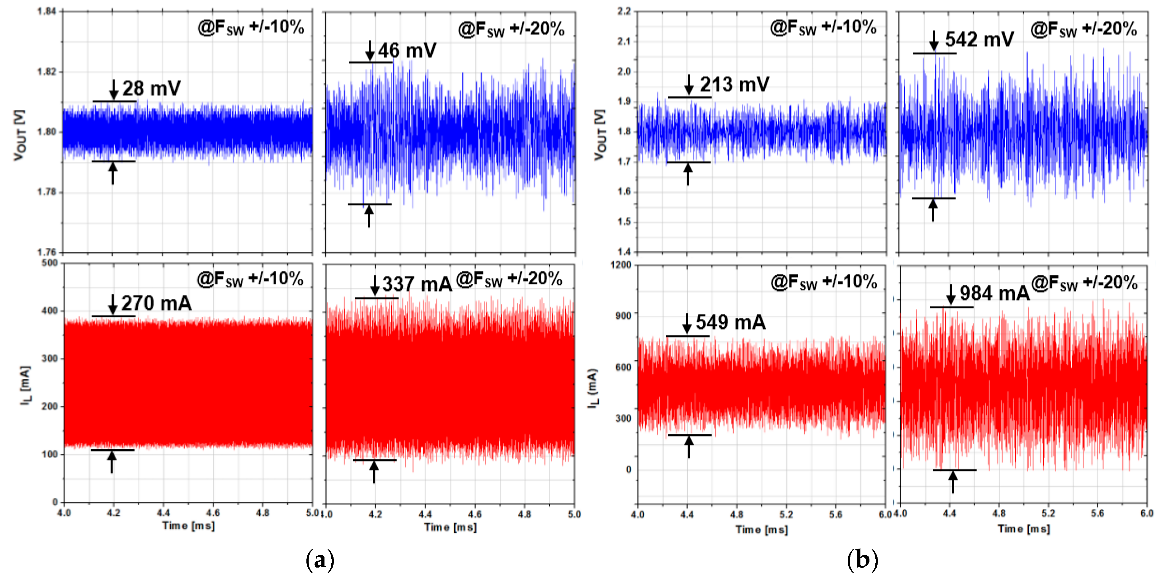
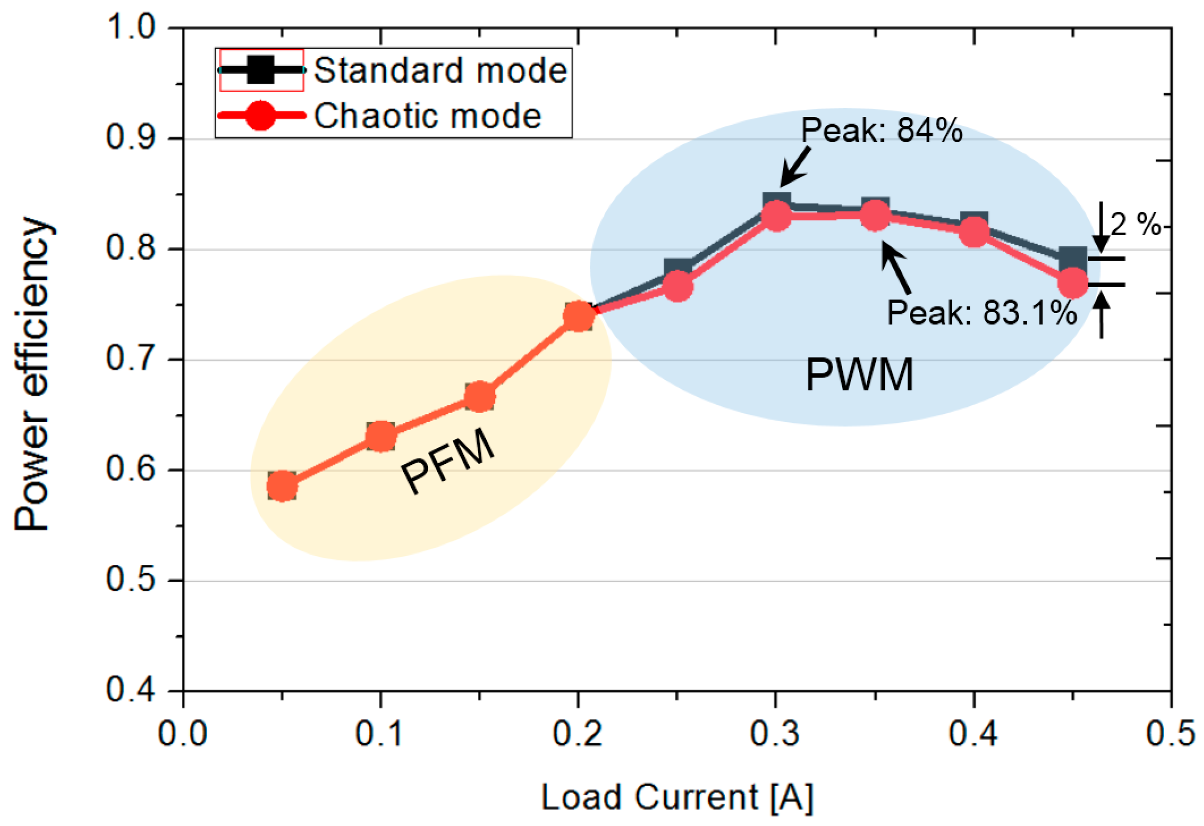
4.2. Reducing the Side Effects of the Proposed EMI-Improvement Scheme

The main purpose of a DC-DC converter is power conversion; therefore, the power efficiency of a converter must be maintained in a reasonable range whatever EMI reduction technique is used. Figure 20 shows the measured power efficiency at different load currents. The maximum power efficiencies of the converters are 84% and 83.1% for the fixed-frequency PWM mode and chaotic PWM mode, respectively. There is no difference in the power efficiency between the two PFM modes because they are common and are not included in EMI reduction. When the converter operates in PWM at moderate and heavy loads (200 mA to 450 mA), the power efficiency of the chaotic mode is less than that of the standard mode. The maximum power efficiency degradation is at the maximum load condition of 450 mA, with a reduction of 2% in power efficiency, mainly from the conduction loss, because the average switching frequency of the converter in chaotic mode and fixed-frequency in standard mode is approximately equal. When the converter operates in the chaotic mode, the ripple range of the inductor current increases, which results in an increase in the RMS inductor current. As a consequence, the power loss on the inductor and the on-resistance of the power switches also increases.
Figure 21 shows the measured output voltage ripple in two modes. In this experiment, additional capacitors were added (as shown in Figure 3) to eliminate the high-frequency noises caused by the switching operation of the power switches. The measurements show an output voltage ripple of 38 mV and 16 mV for chaotic mode and standard mode operations, respectively. Compared to the output voltage ripple when the converter operates in PFM mode (Figure 17b), the ripple of the converter in PWM chaotic mode is approximately the same. This can be solved by increasing the capacitor value at the output but that increases the power module and adds additional costs. However, compared to the active EMI reduction with an input filter, this scheme is still much better, and therefore, it can be used for many applications. For a further demonstration, we conducted an experiment in which we increased COUT to 4.7 uF. The output voltage ripple decreased from 38 mV to 27 mV (approximately equal to the output voltage ripple when the converter enters PFM mode at a light load). It should be noted that this might result in instability. As a consequence, the compensation network should be redesigned to balance EMI performance with other factors, depending on the specific application.

5. Conclusions

In this paper, we have proposed and implemented a SiP buck converter with a fully on-chip chaotic triangular ramp generator for EMI reduction. The on-chip chaotic triangular ramp generator is constructed from an N-shaped chaos generator linked with a symmetrical triangular ramp generator. The on-chip chaos generator generates a controllable chaotic signal and applies it to modulate the slope of the triangular signal. The proposed modulated triangular signal based on the N-shaped chaotic circuit is then applied to the spread-spectrum control of a dual-mode PFM/PWM SiP buck converter with EMI reduction. To verify the effectiveness of the proposed scheme, the proposed EMI-improved buck converter was fabricated in a standard 0.18 µm CMOS process, and the experimental results verified the effectiveness of the proposed technique. The proposed scheme experimentally achieved up to 14.53 dB EMI reduction. In the simulation, extending the spread-spectrum bandwidth increased the EMI reduction amount to 19.13 dB with a 20% deviation in the switching frequency. The modulated triangle signal reduces the inductor current imbalance when the converter operates in chaotic mode. Therefore, the magnitude of the output voltage ripple and inductor current ripple of our design is lower than that in other works. This relaxes the required LC value for the output filter of the DC-DC converter. Due to its simplicity of implementation, high EMI improvement, and LC size relaxation, the proposed scheme can effectively solve EMI issues in many applications, especially on-chip and in-package solutions.

Author Contributions

V.H.N. developed the concept and implemented the chip layout. V.H.N. and H.A.H. performed all the experiment, thoroughly analyzed the data and wrote this research article. H.S. and S.K. technically supervised the research work.

Funding

This work was supported by the National Research Foundation of Korea through the Korea Government (MSIP) under Grant NRF-2017R1A2B2003240. This work was also supported by Inje University research grant 2018.

Acknowledgments

The authors would like to thanks Tung Ngoc Nguyen École de Technologie Supérieure, University of Quebec, for his fruitful discussion and guidance. Thanks to IDEC-Korea for their support on CAD tool and chip fabrication.

Conflicts of Interest

The authors declare no conflicts of interest.

References

  1. Disney, D.; Shen, Z.J. Review of silicon power semiconductor technologies for power supply on chip and power supply in package applications. IEEE Trans. Power Electron. 2013, 28, 4168–4181. [Google Scholar] [CrossRef]
  2. Zheng, Y.; Ho, M.; Guo, J.; Leung, K.N. A Single-Inductor Multiple-Output Auto-Buck–Boost DC–DC Converter with Tail-Current Control. IEEE Trans. Power Electron. 2016, 31, 7857–7875. [Google Scholar] [CrossRef]
  3. Joo, J.; Hwang, J.; Song, E.; Kim, S.Y. On-chip layout optimization of synchronous DC-DC buck converter for EMI reduction. In Proceedings of the 2017 IEEE Electrical Design of Advanced Packaging and Systems Symposium (EDAPS), Haining, China, 14–16 December 2017. [Google Scholar]
  4. Edward, N.Y.H.; Philip, K.T.M. Design of PWM ramp signal in voltage-mode CCM random switching frequency buck converter for conductive EMI reduction. IEEE Trans. Circ. Syst. I Reg. Pap. 2013, 60, 505–515. [Google Scholar]
  5. Bhargava, A.; Pommerenke, D.; Kam, K.W.; Centola, F.; Lam, C.W. DC-DC buck converter EMI reduction using PCB layout modification. IEEE Trans. Electromagn. Compat. 2011, 53, 806–813. [Google Scholar] [CrossRef]
  6. Tseng, C.J.; Chen, C.L. A passive lossless snubber cell for non-isolated PWM DC/DC converters. IEEE Trans. Ind. Electron. 1998, 45, 593–601. [Google Scholar] [CrossRef]
  7. Chu, Y.; Wang, S.; Wang, Q. Modeling and stability analysis of active/hybrid common-mode EMI filters for DC/DC power converters. IEEE Trans. Power Electron. 2016, 31, 6254–6263. [Google Scholar] [CrossRef]
  8. Pareschi, F.; Rovatti, R.; Setti, G. EMI reduction via spread-spectrum in DC/DC converters: State of the art, optimization, and tradeoffs. IEEE Access. 2015, 3, 2857–2874. [Google Scholar] [CrossRef]
  9. Lin, F.; Chen, D.Y. Reduction of power supply EMI emission by switching frequency modulation. IEEE Trans. Power Electron. 1994, 9, 132–137. [Google Scholar]
  10. Hardin, K.B.; Fessler, J.T.; Bush, R. Spread spectrum clock generation for the reduction of radiated emissions. In Proceedings of the IEEE Symposium on Electromagnetic Compatibility, Chicago, IL, USA, 22–26 August 1994. [Google Scholar]
  11. Johnson, S.; Zane, R. custom spectral shaping for EMI reduction in high-frequency inverters and ballasts. IEEE Trans. Power Electron. 2005, 20, 1499–1505. [Google Scholar] [CrossRef]
  12. Elrayyah, A.; Namburi, K.M.P.K.; Sozer, Y.; Husain, I. An effective dithering method for electromagnetic interference (EMI) reduction in single-phase DC/AC inverters. IEEE Trans. Power Electron. 2014, 29, 2798–2806. [Google Scholar] [CrossRef]
  13. Davari, P.; Hoene, E.; Zare, F.; Blaabjerg, F. Improving 9–150 kHz performance of single-phase PFC rectifier. In Proceedings of the 10th International conference on integrated power electronics systems (CIPS), Stuttgart, Germany, 20–22 March 2018. [Google Scholar]
  14. Ming, X.; Chen, Z.; Zhou, Z.-K.; Zhang, B. An advanced spread spectrum architecture using pseudorandom modulation to improve EMI in class D amplifier. IEEE Trans. Power Electron. 2011, 26, 638–646. [Google Scholar] [CrossRef]
  15. Morcillo, J.D.; Burbano, D.; Angulo, F. Adaptive ramp technique for controlling chaos and subharmonic oscillations in DC-DC power converters. IEEE Trans. Power Electron. 2016, 31, 5330–5343. [Google Scholar] [CrossRef]
  16. Li, H.; Li, Z.; Zhang, B.; Wang, F.; Tan, N.; Halang, W.A. Design of analogue chaotic PWM for EMI suppression. IEEE Trans. Electromagn. Compat. 2010, 52, 1001–1007. [Google Scholar] [CrossRef]
  17. Li, H.G.; Gong, S.D.; Liu, J.W.; Su, D.L. CMOS-based chaotic PWM generator for EMI reduction. IEEE Trans. Electromagn. Compat. 2017, 59, 1224–1231. [Google Scholar] [CrossRef]
  18. Huynh, H.A.; Han, Y.; Park, S.; Hwang, J.; Song, E.; Kim, S. Design and analysis of the DC-DC converter with a frequency hopping technique for EMI reduction. IEEE Trans. Compon. Packag. Manuf. Technol. 2018, 8, 546–553. [Google Scholar] [CrossRef]
  19. Tsai, J.; Huang, T.; Lai, W.; Chen, K. Dual modulation technique for high efficiency in high-switching buck converters over a wide load range. IEEE Trans. Circ. Syst. I Regul. Pap. 2011, 58, 1671–1680. [Google Scholar] [CrossRef]
  20. Ma, F.F.; Chen, W.Z.; Wu, J.C. A monolithic current-mode buck converter with advanced control and protection circuits. IEEE Trans. Power Electron. 2007, 22, 1836–1846. [Google Scholar] [CrossRef]
  21. Mattingly, D. Designing Stable Compensation Networks for Single Phase Voltage Mode Buck Regulators. Available online: www.intersil.com/data/tb/tb417.pdf (accessed on 11 October 2018).
  22. Kim, E.J.; Cho, C.H.; Kim, W.; Lee, C.H.; Laskar, J. Spurious noise reduction by modulating switching frequency in dc-to-dc converter for RF power amplifier. In Proceedings of the 2010 IEEE Radio Frequency Integrated Circuits Symposium, Anaheim, CA, USA, 23–25 May 2010. [Google Scholar]
  23. Juncu, V.D. Integrated circuit implementation of a compact discrete-time chaos generator. Analog Integr. Circuits Signal Process. 2006, 46, 275–280. [Google Scholar] [CrossRef]
  24. Lin, Y.; Wang, C. Current-mode multi-scroll chaos generator employing CCCII. Electron. Lett. 2016, 52, 1295–1297. [Google Scholar] [CrossRef]
  25. Wu, Y.L.; Yang, C.H.; Wu, C.H. Chip implementation of a new hyperchaotic oscillator. Electron. Lett. 2017, 53, 226–228. [Google Scholar] [CrossRef]
  26. Sano, M.; Sawada, Y. Measurement of the Lyapunov spectrum from a chaotic time series. Phys. Rev. Lett. 1985, 55, 1082–1085. [Google Scholar] [CrossRef] [PubMed]
  27. Nguyen, V.H.; Kumar, S.; Song, H.J. A family of fully integrated CMOS chaos generators with strictly 1-D linear-piecewise chaos maps. J. Comput. Electron. 2018, 17, 1343–1355. [Google Scholar] [CrossRef]
  28. Nashed, M.; Fayed, A.A. Current-mode hysteretic buck converter with spur-free control for variable switching noise mitigation. IEEE Trans. Power Electron. 2018, 33, 650–664. [Google Scholar] [CrossRef]
  29. Cheng, L.; Liu, Y.; Wing-Hung, K. A 10/30 MHz fast reference-tracking buck converter with DDA-based type-III compensator. IEEE J. Solid-State Circ. 2014, 9, 2788–2799. [Google Scholar] [CrossRef]
  30. Aruna, P.; Premalatha, L. Investigation of EMI reduction in buck converter by using external chaos generator. In Proceedings of the 2011 International conference on recent advancements in electrical, electronics and control engineering, Sivakasi, India, 15–17 December 2011. [Google Scholar]
Figure 1. System-in-package (SiP) buck converter with chaos-based electromagnetic interference (EMI) reduction. The highlighted chaotic ramp and clock generator forces the converter to operate in chaotic mode for EMI reduction.
Electronics 07 00254 g001
Figure 2. Proposed scheme for synthesizing a chaotic pulse-width modulation (PWM) signal with an N-shaped chaotic generator for a buck converter using a type-III compensator network.
Electronics 07 00254 g002
Figure 3. Simplified block diagram of the proposed N-shaped chaos generator.
Electronics 07 00254 g003
Figure 4. Operation of the N-shaped-based chaos generator: (a) Finite state machine. (bd) Capacitor voltage waveform.
Electronics 07 00254 g004
Figure 5. Bifurcation diagram versus T2 of the mathematical model of the proposed N-shaped chaos generator. The range of T2 associated with the dense area of the diagram shows chaotic behavior and can be used later to design Complementary Metal Oxide Semiconductor (CMOS) chaotic circuit.
Electronics 07 00254 g005
Figure 6. Proposed design of chaotic triangular ramp generator: (a) Chaotic ramp generator; (b) N-shaped chaos generator.
Electronics 07 00254 g006
Figure 7. Modulation of chaotic triangular ramp signal: (a) peak modulation; (b) slope modulation.
Electronics 07 00254 g007
Figure 8. Steady-state time-domain simulation results of the converter in chaotic mode using chaotic triangular ramp generator with slope modulation.
Electronics 07 00254 g008
Figure 9. Operation mode of buck converter under phase-portrait view between two internal states (output voltage and inductor current): (a) Standard mode. (b) Chaotic mode.
Electronics 07 00254 g009
Figure 10. Simulated distribution of the switching frequency in chaotic mode using slope modulation: (a) 1.2 MHz +/− 10% (1.08 MHz to 1.32 MHz); (b) 1.2 MHz +/− 20% (0.96 MHz to 1.44 MHz).
Electronics 07 00254 g010
Figure 11. Simulated power spectrum in chaotic mode (with slope modulation) with FSW +/− 10% (1.08 MHz to 1.32 MHz): (a) Output node; (b) Switching node (@VDD = 3.0 V, Vo = 1.8 V, Io = 500 mA, L = 2.2 μH, C = 2.2 μH).
Electronics 07 00254 g011
Figure 12. Simulated power spectrum in chaotic mode (with slope modulation) with FSW +/− 20% (0.96 MHz to 1.44 MHz): (a) Output node; (b) Switching node (@VDD = 3.0 V, Vo = 1.8 V, Io = 500 mA, L = 2.2 μH, C = 2.2 μH).
Electronics 07 00254 g012
Figure 13. Simulated output voltage and inductor current waveform in chaotic mode: (a) Using ramp generator with slope modulation; (b) Ramp generator with peak modulation. Standard mode: VOUT_ripple: 13.36 mV, IL_ripple: 257 mA (@ Simulation condition: Io = 250 mA). (FSW +/− 10% (1.08 MHz to 1.32 MHz); FSW +/− 20% (0.96 MHz to 1.44 MHz)).
Electronics 07 00254 g013
Figure 14. (a) Chip layout of the chaotic-PWM (pulse-width modulation) voltage-mode buck converter; (b) Chip microphotograph; chip test on printed circuit board (PCB) (the top).
Electronics 07 00254 g014
Figure 15. Experimental setup of the monolithic EMI-improved SiP buck converter. R is the current biasing current resistor of the V-I converter for the triangular ramp generator, and the VBR, VHC, and VLC of the triangular ramp generator are easy to tune.
Electronics 07 00254 g015
Figure 16. Measurement result of the chaotic ramp generator: (a) Standard mode: triangular ramp generator with fixed switching frequency of 1.2 MHz (1.214 MHz); (b) Chaotic mode: ramp generator with chaotic switching frequency at FSW +/− 20%. (Channel 1: VBR; Channel 2: clock impulse signal. The width of measured impulse: ~15 ns; (X: 4 us/div, Y: 0.3 V/div)).
Electronics 07 00254 g016
Figure 17. Measurement results for the fabricated chip in standard mode: (a) PWM mode (IOUT = 250 mA); (b) pulse-frequency modulation (PFM) mode (IOUT = 150 mA).
Electronics 07 00254 g017
Figure 18. Measurement result of the fabricated chip: (a) Inductor current of the standard mode (top) and chaotic mode (bottom) (measurement mode: AC coupling @DC level: 0 V); (b) Power spectrum calculation results.
Electronics 07 00254 g018
Figure 19. Conducted emission measurement of the buck converter.
Electronics 07 00254 g019
Figure 20. Measured power conversion efficiency at standard fixed-frequency mode and chaotic frequency mode with FSW +/− 10%. The maximum power efficiency reduction of 2% is at 450 mA of load current.
Electronics 07 00254 g020
Figure 21. Measurement of output voltage ripple: (a) Chaotic mode and (b) Fixed-frequency mode (Measurement Mode: AC coupling @ DC level: 0 V).
Electronics 07 00254 g021aElectronics 07 00254 g021b
Table 1. Designed buck converter specifications.
ParameterDescriptionQuantity
VINInput voltage range (Battery)2.7–4.2 V
VOUTOutput voltage range1.0–1.8 V
IOUT,maxMaximum load current500 mA
Vrip,(max)Maximum output ripple50 mV
FSWSwitching frequency1–2 MHz
LOUTInductor (in package)2.2 μH
COUTOutput capacitor (in package)2.2 μF
Table 2. List of component values used in test setup.
ParameterQuantity
CIN10 μF
LOUT2.2 μH
COUT2.2 μF
RFB14.3 kΩ
(*) RFB29.47 kΩ
C115 pF
C21 nF
C3470 pF
R14.7 kΩ
R2560 Ω
(*) RFB2: Controlled by a variable resistor (internal VREF: 1.238 V).
Table 3. EMI reduction performance of the proposed scheme and stage-of-the-art alternatives.
Ref.Implementation MethodModulation TechniqueEMI ReductionSwitching FrequencyCompatibility for On-Chip Integration
[17]CMOS
@ 0.35 μm
Random PWM12.85 dB0.89–1.44 MHzSuitable
[18]CMOS
@ 0.18 μm
Random PWM
(Frequency hopping)
12.6 dB1.4–2.1 MHzSuitable
[19]HybridChaotic PWM10 dB 160 +/− Δf 2No
This workCMOS
@ 0.18 μm
Chaotic PWM14.53 dB1.04–1.31 MHzSuitable
1 Extracted from figure; 2 Δf is not determined.

