1. Introduction
Gallium nitride (GaN) has been well recognized as the material whose electrical parameters are ideally suited for power devices as well as high frequency devices [
1]. Horizontal structured GaN power-switching devices such as Metal-Insulator-Semiconductor Field Effect Transistor (MISFET) are already been commercially available. However, their power conversion efficiency and current drivability are limited because of their very high lattice-misfit dislocation densities which are caused by hetero-epitaxy on foreign substrates such as Si and SiC. Recent progress in crystalline quality and productivity of free-standing GaN substrates has enabled rapid development of vertical structure devices, which can extract the GaN’s full potentials in power-conversion applications [
2,
3,
4].
For p-n junction diodes, the electric field becomes high at the p-n interface, depletion layer edges and electrode edges when a high reverse voltage is applied. So the breakdown voltage is determined by the electric field of the edges. To decrease the edge electric field of the device, edge termination techniques are important in designing high voltage power devices. Some techniques have been applied to the GaN diodes with high breakdown voltage to reduce their maximum electric field. These techniques are mesa-etched edge termination, guard rings and field plate (FP) termination [
5,
6,
7]. Although the maximum electric field of the GaN diodes can be decreased by FP termination, the peak electric field is still located at the edge [
8,
9].The thickness of the dielectric film affects the depth of the depletion region. Thin dielectric film is effective for the breakdown characteristics within the p-n junction, but as a result, the electric field in the dielectric film becomes higher, and then breakdown tends to occur near the field-plate edge on the dielectric film. Our approach for increasing breakdown voltage using FP termination is to use high-dielectric-constant films. A high-dielectric-constant film generates a greater expanded depletion region than that generated using SiO
2 film of the same thickness. Therefore, higher breakdown voltage devices are expected.
In this study, we used high-k mesa-etched GaN diodes with FP termination. To improve breakdown characteristics, we tried to determine the optimum dielectric constant for mesa-etched GaN diodes from the simulated result. Furthermore, we fabricated diodes that were immune to avalanche breakdown.
2. Device Structure and Fabrication Process
Figure 1 shows the schematic cross-section of the p-n diode simulated and fabricated in this study. The layer structure was grown by metal–organic vapor phase epitaxy (MOVPE) on a free-standing GaN substrate. The epitaxial layers consist of p
+-GaN (Mg: 2 × 10
20 cm
−3, 30 nm)/p-GaN (Mg: 1 × 10
18 cm
−3, 500 nm)/n
—GaN (Si: 3 × 10
15 cm
−3, 1 μm)/n-GaN (Si: 1.1 × 10
16 cm
−3, 17 μm)/n-GaN (Si: 2 × 10
18 cm
−3, 2 μm). The mesa structure was fabricated by inductively-coupled plasma (ICP) dry-etching. Pd ohmic electrodes were deposited by electron-beam deposition and formed by a liftoff process on the surface of the p
+-GaN layer. Passivation film (SOG (spin-on-glass)/SiO
2 or mixed oxide of CeO
2 and SiO
2) with the thickness of 700 nm was deposited on the top excluding the surface of the Pd contact. Contact holes were formed by ICP dry-etching. A Ti/Al electrode as a field plate was deposited by electron-beam deposition and formed by a liftoff process on the top surface [
10]. The Ti/Al electrode was deposited by electron-beam deposition on the bottom surface of the n-GaN substrate.
We have fabricated different types of insulators as a passivation film. One type is SOG/SiO
2. SOG insulating film was deposited on the whole chip. The SOG film was annealed at 450 °C for 30 min in the ambient N
2. Then, a SiO
2 insulating film was deposited on the whole chip by sputtering. We developed a two-step process for anode electrodes in order to avoid plasma damage to the p+-GaN contact layer during the SiO
2 sputtering process. The specific ON-resistance is further improved due to a new low-damage process [
8,
9]. The other type is a mixed oxide of CeO
2 and SiO
2. We deposited a mixed oxide of CeO
2 and SiO
2 using Metal Organic Chemical Vapor Deposition (MOCVD) with the compositional ratio of CeO
2:SiO
2 = 2:1 [
11,
12,
13]. The deposited dielectric film by MOCVD with intermittent Si(OC
2H
5)
4 introduction was based on the idea that the decomposition temperature of tetraethylorthosilicate (TEOS) can be lowered by the hydrolysis utilizing H
2O generated during the CeO
2 deposition. The CeO
2 source is Ce[OC(C
2H
5)
2CH
3]
4. The CeO
2 source was continuously introduced during deposition for 30 min while TEOS was intermittently introduced for 10 sec every 3 min using the pneumatic cutout valve, according to the deposition cycle. The substrate temperature during deposition was 350 °C and the deposition pressure was 50 Pa. Before deposition, samples were dipped in hafnium (Hf) to remove native oxide on the GaN.
The measured k of mixed oxide of SiO2 and CeO2 with a thickness of 700 nm was 12.3. The structure and thickness of high-k dielectric passivation film were measured using a Scanning Ion Microscope (SIM). As a result of the observation, the side wall of the mesa was a little curved; however, we used linear approximation to obtain convergent results in this simulation. The edge degrees were determined as 60 and 45 degrees from the observation.
We fabricated a GaN diode to obtain its breakdown voltages of 2.0 to 2.5 kV. By reducing the doping concentration underneath the p-GaN layer, the maximum electric field at the p-n junction can be decreased under reverse biased conditions. The GaN diode with a mesa structure can relax the electric field concentration at the p-n junction edge.
3. Simulation
Device simulation was carried out by using the half of the device structure shown in
Figure 1. The simulations were carried out using the TCAD Sentaurus Device from Synopsys Inc. To determine the electric field, Poisson’s Equation is solved. Because the device was bilaterally symmetric (
Figure 1), the simulated model used only the left half of the structure.
Figure 2 shows the simulation results with an FP termination at
k = 3.9, 10, and 100 when a reverse bias of −1 kV is applied to the device. The line interval is 20 V.
Figure 2a shows the simulated equipotential contour distributions when the insulator is SiO
2 (
k = 3.9). The equipotential contours are concentrated on the side wall of the mesa region. Therefore, if a large voltage is applied to the device, the p-n junction at the mesa edge will be destroyed. Next, we increased the value of
k.
Figure 2b shows the simulated equipotential contour distributions when the dielectric constant of the insulator is
k = 10. As shown in the figure, the lines became less dense than in
Figure 2a.
Figure 2c shows the simulated equipotential contour distributions when the dielectric constant of the insulator is
k = 100. While equipotential lines no longer appear on the side wall of the mesa, lines are concentrated at the bottom of the mesa. Therefore, if a large voltage is applied to the device, the bottom of the mesa will be destroyed.
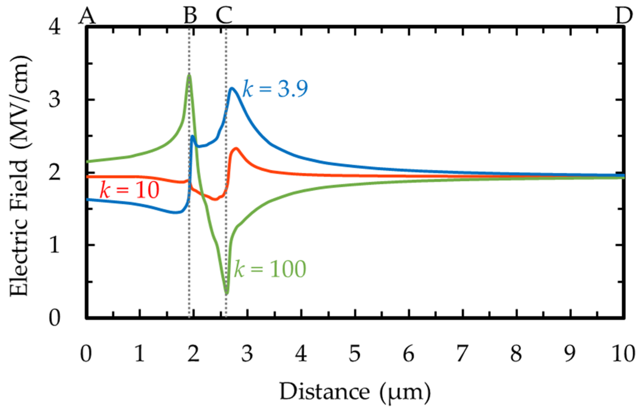
Figure 3 shows the electric field from point A to point D (see
Figure 4) when a reverse bias of −1 kV is applied to the device. The horizontal axis indicates the distance from point A to point D.
Figure 4 shows the enlarged view of the mesa and the p-n junction. Point A is under the insulator. Point B is the bottom of the mesa. Point C is the p-n junction at the mesa edge. Point D is the intrinsic p-n junction. For the diode with an insulator having
k = 3.9 when the insulator is SiO
2, the electric field is shown as a solid line, and it is 1.6 MV/cm at point A and increases at point B and near C, then gradually decreases. The maximum electric field is 3.1 MV/cm near C. Since the diode is destroyed at the point of the highest electric field, we will focus on the peak value of the electric field. There are two peaks, at point B and near point C. At near-C peak, the electric field at the p-n junction reaches its maximum. The electric field between point A and point B is low, but between point B and point D it is high. For
k = 100, the electric field near B is the highest and that at point C is the lowest. For
k = 10, the electric field at point B and the maximum electric field are lower than those of
k = 3.9 and 100.
Figure 5 shows the maximum electric field characteristics of a diode with a different dielectric constant
k of insulators. As shown in the figure, the electric field is dependent on the dielectric constant. At point A, the electric field increases as the dielectric constant increases, but the electric field stays almost the same when the dielectric constant
k is above 10. At point B, the electric field decreases rapidly and reaches the minimum at the dielectric constant
k below 10, and then it gradually increases. At point C, the electric field decreases as the dielectric constant increases. In other words, the maximum electric field at the mesa-etched p-n junction diodes covered with films with a dielectric constant
k value of 10 was reduced to 2.0 MV/cm from 3.1 MV/cm (for SiO
2 of
k = 3.9).
4. Results and Discussion
We selected a mixed oxide of SiO2 and CeO2 for a passivation film in this study. From the simulation results of the reduction of the electric field at the mesa edge, a dielectric constant k of about 10 is appropriate for a mesa-etched diode. The dielectric constant of CeO2 is 26, but can be lowered when SiO2 is mixed in CeO2. CeO2 can easily be deposited on the Si substrate. The capacitance of the mixed oxide of CeO2 and SiO2 is 15 nF/cm2. Assuming the thickness of the mixed oxide is 700 nm, we calculated the dielectric constant k of the mixed oxide as 12.3 at 1 MHz. The measured breakdown electric field of CeO2 is 1.8 MV/cm. The mixed oxide was not measured. However, the breakdown electric field of the mixed oxide of SiO2 and CeO2 is higher than that of CeO2. Therefore, the breakdown electric field of the mixed oxide is greater than 1.8 MV/cm.
Figure 6 shows the forward bias characteristics of the diodes with SiO
2/SOG and the mixed oxide of SiO
2 and CeO
2. The turn-on voltage was about 3 V and Ron was 0.3 mΩ·cm
2 (@5 V) for both diodes. In the log-scale plots (not shown), ideality factors were close to 2. Although the forward characteristics were the same, the reverse ones were apparently different.
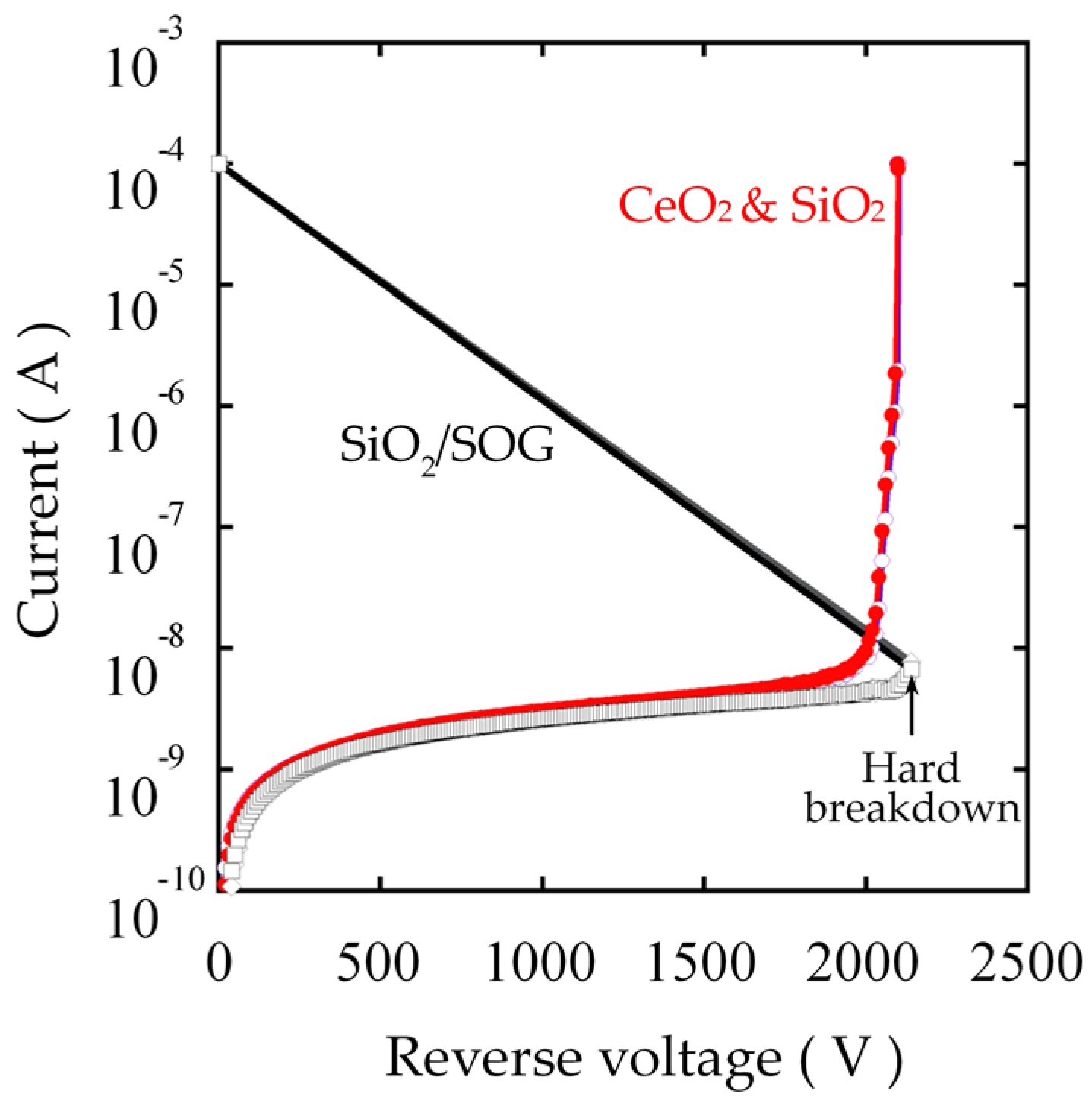
Figure 7 shows the reverse bias characteristics of the diodes with SiO
2/SOG and the mixed oxide of SiO
2 and CeO
2.
Figure 7 represents characteristics of two diodes for each of the GaN diodes with the different dielectrics. So, four curves were plotted in
Figure 7. We made measurements on several diodes within each chip and found almost significant results; hence, we left the four curves in
Figure 7 to avoid complexity. Breakdown voltage (BV) characteristics were evaluated using Agilent B1505A combined with an ultra-high-voltage unit at room temperature. The expected breakdown voltage calculated by Poisson’s Equation using the layer structure was 2.0–2.5 kV assuming the GaN’s breakdown field is about 3.3 MV/cm. The measured breakdown voltage was close to the calculated values. I–V characteristics of the diode covered with the mixed oxide showed a breakdown voltage of 2.2 kV with an increased avalanche capability. While breakdown characteristics of the diode covered with SiO
2/SOG showed the same breakdown voltage, the diode was suddenly broken at the same voltage (2.2 kV). This means that the electric field reduces at the periphery of the mesa-etched p-n junction and was uniformly formed across the whole p-n junction. When a higher dielectric film passivation is used, uniform reverse current flows and avalanche breakdown–immune diode characteristics can be obtained. It is clear that high-k dielectric film passivation and field plate termination are essential techniques for GaN power devices.


