Article

Power Amplifier Modeling Framework for Front-End-Aware Next-Generation Wireless Networks

by
Kornelia Kostrzewska
and
Pawel Kryszkiewicz
*
Institute of Radiocommunications, Poznan University of Technology, 60-965 Poznan, Poland
*
Author to whom correspondence should be addressed.
Electronics 2024, 13(9), 1643; https://doi.org/10.3390/electronics13091643
Submission received: 20 March 2024 / Revised: 22 April 2024 / Accepted: 23 April 2024 / Published: 25 April 2024
(This article belongs to the Section Computer Science & Engineering)

Abstract

:
Next-generation wireless systems require increased spectral and energy efficiency in terminals. This can only be achieved if the nonlinear characteristics of the radio front-end, primarily the power amplifier (PA), are known and considered while designing algorithms or optimizing radio links. PA datasheets contain limited information, and wideband PA measurements typically require advanced equipment and software. This paper proposes a measurement and signal processing framework that enables the acquisition of nonlinear PA characteristics using generic complex sample transmitters and receivers, e.g., software-defined radio (SDR). This paper also proposes a multistage signal calibration and synchronization procedure that allows obtaining nonlinear PA characteristics that are non-distorted by other phenomena. The correctness and usefulness of the proposed framework are demonstrated by measuring three PAs, each under varying supply voltage and carrier frequency. At the same time, the high variability of the obtained nonlinear characteristic justifies the need for PA measurements to obtain awareness of nonlinear characteristics.

1. Introduction

Wireless communication is becoming more popular. This increase is associated with the need to provide increasing data rates to meet the demands of users. One of the latest proposals to meet the growing requirement is 5G technology. It increases the capacity of the system by more than 1000 times and boosts cell throughput by over 25 times while improving spectral efficiency by more than 10 times compared to previous 4G technologies [1]. Even higher performance will probably be achieved by a 6G system [2].
Still, this continuous increase in transmission speed results in increased requirements on the hardware performance, e.g., bandwidth, and receiver sensitivity. At the same time, it is expected that new transceivers will be highly energy-efficient [3]. Most importantly, up to 80% of energy consumption at the base station can be attributed to the power amplifier [4]. In the case of a PA, the highest signal quality, characterized by minimal self-distortion, is obtained when the PA is linear in the whole range of transmitted signal samples. While an orthogonal frequency division multiplexing (OFDM) waveform used in 4G and 5G systems exhibits high variations in instantaneous power (typically measured using the peak-to-average power ratio (PAPR)), the linearity of the power amplifier (PA) must be maintained across a wide range of amplitudes. At the same time, the energy efficiency (EE) of a given PA can be compromised. For this reason, various PA architectures have been proposed to fulfill both requirements simultaneously, with Envelope Tracking (ET) being one of the most successful approaches recently [5]. From this perspective, it is foreseen that new transceiver designs will have to balance energy and spectral efficiency, potentially by enabling front-end awareness of the signal processing and radio control algorithms, with the most basic one being digital pre-distortion (DPD) [6]. In this case, an important issue for the transceiver will be to have an accurate model of power consumption and amplifier input–output characteristics.
However, modeling PA characteristics is a complex task [7]. First, broadband measurements, with a bandwidth wider than the bandwidth of the intended transmission, are necessary to observe spectral regrowth effects. In addition, this allows a measurement of possible memory effects, which may noticeably affect the quality of the transmission. The type of transmitted signal is also significant, as it may lead to different PA behaviors. The safest approach is to apply a realistic signal, which is most likely to be transmitted later, like wideband code division multiple access (WCDMA) or OFDM. In theory, during behavioral modeling, there is no need for a deep understanding of the underlying radio frequency (RF) circuit physics, functionality, or amplifier construction, as it is simplified to a mathematical formulation that describes the relationship between input and output signals. However, basic knowledge may assist in selecting the appropriate amplifier model. This choice should be deliberate and consider potential difficulties in use and implementation, which may occur with a model that is too complex, as well as the accuracy of the results, which might not be sufficient with simpler models. When modeling the PA’s characteristics, two key aspects must be considered: proper acquisition of signals at the input and output of the device under test (DUT), ensuring their synchronization in time and frequency for accurate behavior analysis, and the formulation of appropriate mathematical equations describing the crucial signal relations. Finally, specialized measuring equipment is needed to adequately receive the output signal.
There are multiple solutions described in the literature. The simplest measurement of gain compression can be obtained using a basic vector network analyzer (VNA) by exciting a PA with a sinusoid of increasing power [8]. However, this is a narrowband measurement unable to reflect memory effects or a different PA response on a standard operation signal, e.g., OFDM. Another common measurement is based on the observation of intermodulation components appearing after exciting PA with a two-tone signal [9]. Although VNA is not needed, it requires, e.g., two transmitters, a signal combiner, and a spectrum analyzer to be used. Still, the obtained PA characteristic might be quite limited. More precise characteristics can be obtained by a nonlinear vector network analyzer [10]. However, this is not a very common device. If built using a four-port VNA, some additional signal generators are needed. As such, the whole setup becomes quite complex. Only the vector signal generator (VSG) and vector signal analyzer (VSA) are required to perform a wideband PA modeling proposed in [8]. While these can be quite expensive devices, the author does not mention synchronization or power calibration procedures. In [11], two digital receivers are used on the input and output of a PA excited by a CDMA2000 signal. The authors do not discuss any synchronization or attenuation mismatch between front ends to be compensated. The problem of synchronization between the transmitter and receiver while characterizing PA characteristics is mentioned in [7,12], although no step-by-step solution or algorithm is proposed.
This paper aims to show that it is possible to achieve broadband amplifier characteristics without using specialized equipment, as long as proper calibration and signal processing are provided. The main contributions of this paper are as follows:
  • A measuring system, which allows testing PAs with the use of a general-purpose IQ-based transmitter and receiver, e.g., SDR;
  • A step-by-step measurement and signal processing solution is provided including cable attenuation compensation, time and frequency synchronization;
  • Algorithms for PA characterization using a polynomial model or Rapp model are provided, although other PA models can be utilized as well;
  • Simulation results confirming high estimation accuracy under varying PA parameters and time/frequency offset;
  • Validation of the framework by measurements and the modeling of three amplifiers for with varying supply voltage and carrier frequency;
The received data are publicly available at [13]. Results demonstrate significant variations in PA characteristics across their carrier frequency and supply voltage, underscoring the necessity of employing the proposed framework to enhance PA awareness.
The paper is organized as follows, Section 2 shows the measurement setup used, taking into account special software/hardware requirements or calibration measurements needed. Section 3 focuses on signal processing proposed to remove all effects other than nonlinearity that influenced the signal on the input and output of the amplifier, considering e.g., amplitude calibration, frequency, and time corrections. Finally, the PA characterization method is proposed, focusing mathematically on two common approaches: the memoryless polynomial and the Rapp model. Section 4 shows the accuracy estimation of the proposed framework employing simulations and an analysis of 3 amplifiers measured. Lastly, the paper is concluded in Section 5.

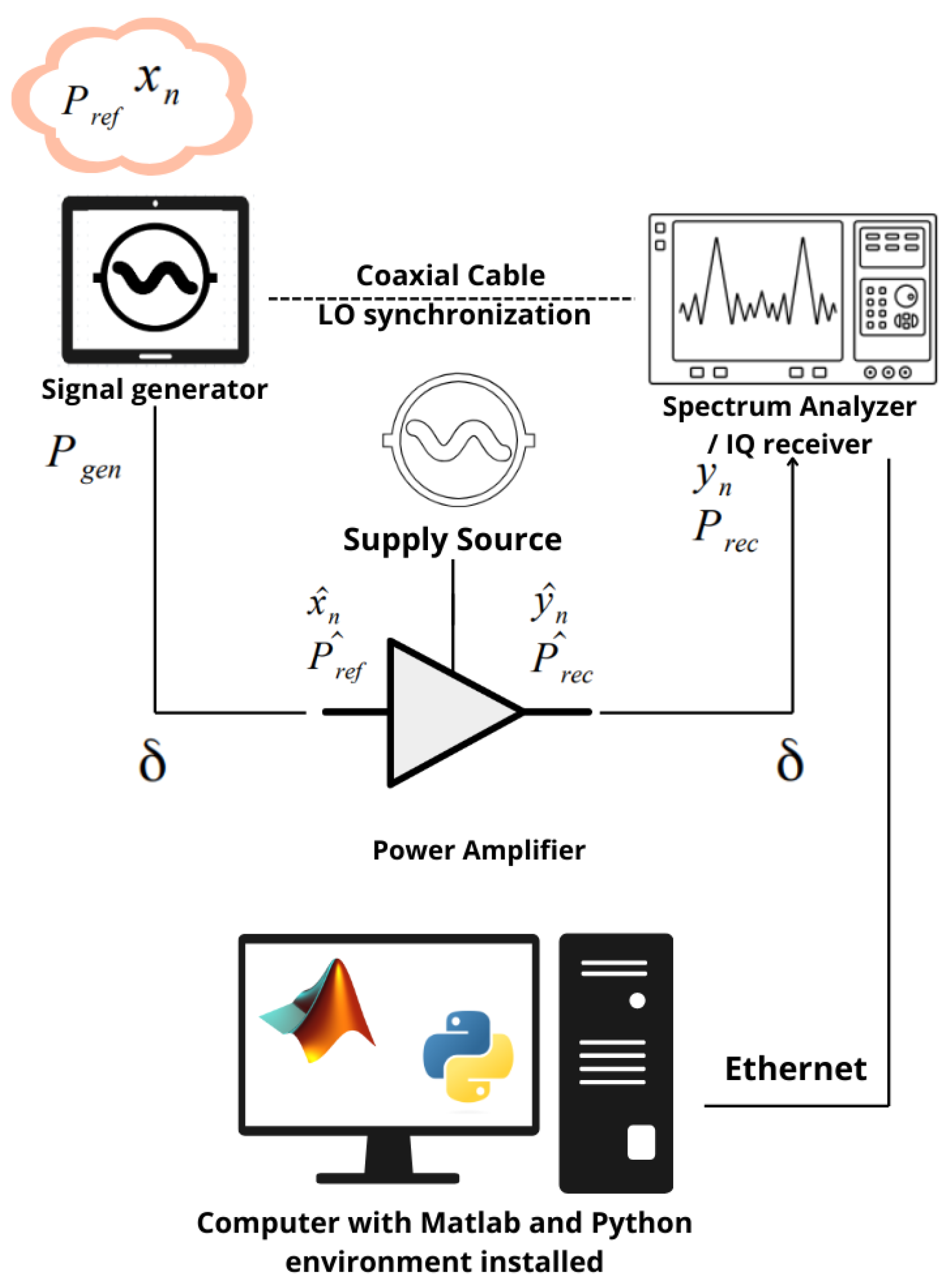
2. Measurement Framework

The measuring setup is shown in Figure 1. It is composed of the following elements:
  • The signal generator.
  • The spectrum analyzer/IQ samples receiver.
  • The power amplifier under test.
  • The supply source.
  • A computer with Matlab and Python environment installed, connected via an Ethernet cable.
It is worth noting that the amplifier under testing can either be a stand-alone device or a series of devices (e.g., a driver amplifier connected serially with a PA) for which a single nonlinearity characteristic will be modeled.
Before proceeding with the measurement, the local oscillators of both the transmitter and the receiver can be locked (if possible) by a coaxial cable, to avoid frequency shifts. However, this is not a required connection as the frequency correction is covered as a part of Section 3.

2.1. Transmitter

The generator should transmit a signal of a similar structure as the one transmitted during standard transmission [7]. We will focus on OFDM symbols, which are the most common nowadays, each consisting of s samples. Assuming L, such symbols are prepared, constituting N = L · s samples, and these are transmitted continuously. It is important to modulate subcarriers far from the band edges (around the direct current (DC) subcarrier) to prevent distortion on digital-to-analog and analog-to-digital converters (DAC/ADC). The transmitter power should be strong enough to drive the measured PA into its nonlinear region. Simultaneously, the generator should operate in its linear region, which can be confirmed by measuring the linearity of the setup without the PA on the transmitter-receiver link. Most importantly, the transmit power must be known, i.e., a calibrated transmitter is used, or initial measurements are made using a spectrum analyzer or power meter.

2.2. Receiver

To capture the noisy samples from the PA output, a receiver with sufficient bandwidth, possibly around four times wider than the bandwidth occupied by the transmitted subcarriers [7], and capable of saving IQ samples should be used. One option is to use a proper spectrum analyzer with an IQ sample reception option enabled. Keeping in mind that the transmitted signal is periodic with a duration of N samples, the measured vector of IQ samples from the spectrum analyzer must have a length of at least 2N. This assures that one full period of the signal will be received, which, after appropriate corrections, can be used for further analysis. To properly collect samples, the receiver must operate within its linear region. It can be obtained by setting its internal attenuator to a sufficiently high level or adding an external attenuator at the receiver input.
The samples taken into the MATLAB environment are in the form of raw IQ samples, which allow for the analysis of the baseband signal using complex values. The use of these complex values enables basic pass signal analysis and is commonly used in many research studies on signal analysis or modeling [12,14,15]. While reading IQ samples is not a common feature in spectrum analyzers, the used R&S FSL6 can perform this action. The resulting I/Q samples are linearly scaled values in Volt units, corresponding to the voltage at the instrument’s RF input, as specified by the manufacturer in the device manual [16].

3. Signal Processing

3.1. Pre-Calibration

Before proceeding with the signal processing, several obstacles must be taken into consideration.
First, the attenuation of cables affects the power both on the input and the output of the PA. For the coaxial cables, as the attenuation typically depends on the frequency at which the signal was transmitted, it should be obtained directly at the utilized carrier frequency. The attenuation was measured by connecting the transmitter and receiver with two identical cables in series and subtracting the received power when only one cable was used. Thanks to this, a measured value of attenuation for one cable, δ , was obtained.
While the samples at both the transmitter and receiver are saved as files with digital IQ samples, typically unitless, it is important to scale them properly to represent the same units, e.g., volts. As such, it can be assumed that virtual amplification occurs at the signal generator. Let the time domain signal prepared for transmission be represented by a vector of digital samples, x , with n samples, where n { 0 , , N 1 } .
This signal average power can be expressed as follows:
P r e f = 1 N n = 0 N 1 | x n | 2 50 .
with units of watts, while x n has units of volts. This is a standard formula for the power of the sampled signal, divided by 50 Ohm, the matching resistance of the RF components. This formula aligns with the signal representation used in the spectrum analyzer R&S FSL6 [16]. Recall that the signal is purely digital, so its power is “virtual”. However, at the output of the signal generator, it is mapped to a continuous signal of a given power, P g e n , in watts. This mapping can be modeled by a virtual amplification of the signal inside the signal generator, expressed by the following:
G 1 = P g e n P r e f .
Observe that this is an amplitude gain, not a power gain.
To obtain the signal x ^ and its average power P ^ r e f at the amplifier input, it is sufficient to remove the cable attenuation from the average power at the output of the generator P g e n . If its value in the dB scale equals δ , the average power at the input of the amplifier, P ^ r e f , can be calculated from the following formula:
P ^ r e f = P g e n · 10 δ 10 .
However, cable attenuation and virtual gain must still be taken into account in the samples themselves. This is possible by multiplying the transmitted signal x by G 1 (2), and the corresponding attenuation value converted to a linear scale:
x ^ n = G 1 · x n · 10 δ 20 .
As a result, we obtained the signal at the amplifier input. In order to obtain the amplifier’s characteristics, the signal at the amplifier’s output also needs to be calibrated.
A signal vector y is known at the input of the analyzer with y n being the n-th sample, where n { 0 , , N 1 } , N > = 2 N . Its average power, P r e c , is calculated according to the following formula:
P r e c = 1 N n = 0 N 1 | y n | 2 50 .
Its digital samples should be scaled to represent volts. If a device with a non-calibrated IQ samples scale is used, a trick with virtual gain, as described above for the generator, can be used. To obtain the signal y ^ at the output of the amplifier, the attenuation introduced by the cable supplying the signal to the analyzer must be taken into account. This comes down to scaling the y signal by the cable attenuation using the following formula:
y ^ n = y n · 10 δ 20 .
The average power of the received signal y ^ in dBm is calculated on the same basis as the average power of the reference signal (e.g., (3)) and presented in the following equation:
P ^ r e c = P r e c · 10 δ 10 .

3.2. Correction

At this stage, the vectors x ^ and y ^ refer to the signal on the input and output of the amplifier, respectively. Still, the received samples might be shifted both in time and frequency. So, the signal at the output of the amplifier can be modeled as follows:
y ^ n = g x ^ n Δ t e j 2 π Δ f ( n Δ t ) ,
where g ( x ^ n Δ t ) is the distortion function of the amplifier, Δ t refers to the time shift, and Δ f refers to the frequency shift.
The proposed correction procedure is based on multiple algorithms, influenced primarily by [14,17]. It consists of four stages:
  • Coarse frequency correction.
  • Coarse time correction.
  • Fine frequency correction.
  • Fine time correction.
While some of the stages can be evaluated in different orders without influencing synchronization quality, some others require previous stages to be completed, e.g., fine time correction. The aim of this section is to provide a step-by-step synchronization algorithm that provides sufficient performance for the PA modeling to be accurate.
At the beginning, the discrete Fourier transform (DFT) is calculated for both x ^ and y ^ signals, according to the following equations:
X ^ k = n = 0 N 1 e 2 π j k n N x ^ n ,
Y ^ k = n = 0 N 1 e 2 π j k n N y ^ n .
where N stands for the DFT size, n represents the sample number in the time domain, and k is the sample number in the frequency domain.

3.2.1. Coarse Frequency Correction

This part aims to find an offset that is greater than subcarrier spacing. While this stage is not necessary because of synchronization between the transmitter and the receiver, it is described for the algorithm’s completeness. Coarse frequency correction is performed using the following formula:
Δ f i n t = a r g max Δ f 1 k H | X ^ k | 2 0.01 max k | X ^ k | 2 Y ^ k Δ f 1 2 ,
where k 0 , , N 1 denotes the subcarrier index, and  Δ f 1 refers to the tested frequency offset. The function used, H ( x ) , is a Heaviside step function, which equals 1 when x is greater than or equal to 0, and 0 otherwise. In this case, the argument of the Heaviside step function results in 1 when the magnitude of a given sample squared is greater than one-hundredth of the magnitude of the largest sample of that signal squared. Finally, the function returns a mask of occupied subcarriers in the transmitted signal, where 0 indicates the subcarrier is not used and 1 indicates that it is occupied.
To apply the determined offset to the received signal, the following steps are used:
  • In the frequency domain: shift the sample set of signal Y ^ k to the left by the found frequency offset Δ f i n t .
    Y ˙ k = Y ^ k Δ f i n t ,
  • In the time domain: mix the received signal with a complex sinusoid of frequency Δ f i n t .
    y ˙ n = y ^ n · e j 2 π Δ f i n t n N ,
    where Δ f i n t represents the determined offset, n stands for the number of the currently considered sample in y ^ , and N is the total number of samples in x ^ .

3.2.2. Coarse Time Correction

To determine the coarse time offset, the shift theorem for DFT is used. This theorem states that the cyclic time shift by m samples is equivalent to a phase shift in the frequency domain, as expressed by the following formula:
F { x n m } k = X k · e j 2 π k m N ,
where F ( { x n m } ) k represents a Fourier Transform result on the k-th subcarrier, computed for x , a signal shifted in time by m samples. After transformation, it is represented as follows:
e j 2 π k m N = F { x n m } k X k
where the shifted transmitted signal refers to the received signal Y ˙ k . Note that the result for each subcarrier, combined with the absolute value of the means of the inverse discrete Fourier transform (IDFT), estimates the time shift as Δ t i n t , representing a shift in an integer number of OFDM symbol samples. Since for n = m all summed complex numbers are added in phase, this maximizes the result. Consequently, the coarse time offset can be expressed as follows:
Δ t i n t = a r g max n 1 N k = 0 N 1 Y ˙ k X ^ k e j 2 π k n N ,
where N stands for the IDFT size, n represents the sample number in the time domain, and k represents the sample number in the frequency domain.

3.2.3. Fine Frequency Correction

To initiate the estimation of the fractional frequency offset Δ f f i n e , the correlation between the reference signal x ^ and the conjugation of received signal y ˙ , shifted by Δ f 2 , is determined as follows:
Δ f f i n e = a r g max Δ f 2 n = 0 N 1 x ^ n y ˙ n + Δ t i n t * e j 2 π n Δ f 2 N .
Theoretically, the  Δ f 2 should be in the range of 0.5 , 0.5 (normalized frequency with respect to the OFDM subcarrier spacing) as the integer frequency offset has already been compensated. The golden-section search, a technique for finding an extremum of a function inside a specified interval, was used to find the fractional frequency offset.
At this stage, armed with the knowledge of the integer offset Δ f i n t and fractional offset Δ f f i n e , the total frequency offset Δ f a l l of the received signal can be calculated,
Δ f a l l = Δ f i n t + Δ f f i n e
Since the integer offset Δ f i n t has already been compensated for the signal, y ˙ requires only a shift by Δ f f i n e :
y ˇ n = y ˙ n · e j 2 π Δ f f i n e n N .

3.2.4. Fine Time Correction

In the final step, the estimation of the subsample time offset Δ t f i n e is conducted using the Lagrange polynomial approximation on 2 M + 1 samples [18].
Initially, it is necessary to define the vector z , which contains the results of the correlation between the conjugated reference signal x ^ and shifted received signal y ˇ :
z i = n = 0 N 1 y ˇ n + Δ t i n t + i M · x ^ n * ,
where i { 0 , , 2 M } .
Firstly, 2 M + 1 Lagrange polynomials are determined, where the i-th polynomial, denoted as l i ( t ) , has value 1 only for t = i M and zeros for t = j M and j { 0 , , i 1 , i + 1 , , 2 M } . Next, these polynomials of degree M 1 are scaled and added to interpolate the correlation function, resulting in the following:
l ( t ) = i = 0 2 M z i l i ( t ) .
The searched fractional time shift is equal to the real root of the first derivative of the polynomial l ( t ) , closest to the sample Δ t i n t , as follows:
Δ t f i n e = a r g min r | r : l ( r ) = 0 | .
The closing step involves determining the vector of the Lagrange polynomial values l i ( Δ t f i n e ) , which will be used to interpolate the signal y ˇ n to obtain its version shifted by Δ t f i n e samples. The offset will be applied by iteratively multiplying the samples by the values of the Lagrange polynomial coefficients l j ( Δ t f i n e ) , as follows:
y n ´ = i = 0 2 M y ˇ n + Δ t i n t + i M · l i ( Δ t f i n e ) ,
for n 0 , N . While the signal y ˇ ( n ) still contains more samples than the reference signal, the range of n in the above equation was limited to obtain only N received samples.
At this point, the entire correction in the frequency and time domain of the received signal is completed and applied to vectors. The diagram summarizing the individual steps is presented in Figure 2.

3.3. PA Modeling

Various models parameterize the characteristics of amplifiers and their nonlinearity. These models can be distinguished based on whether they account for the memory effect, such as the Volterra series, Wiener, or Hammerstein models, or if they only characterize static nonlinearities, like those by Saleh, Rapp, or Ghorbani [19]. Considerable effort has been devoted to reviewing, analyzing, or comparing basic available models such as [1,4,7]. However, for contemporary, solid-state power amplifiers used in 5G systems, the Rapp model has been proposed [20]. The Rapp model has a low number of parameters, introducing only amplitude distortion or mild AM/PM distortion in an extended form [20], but can describe the most significant effects of nonlinear distortion. Moreover, as pointed out in [21], it is one of the most commonly used nowadays, as shown by the number of citations, and can be easily extended, e.g., to reflect AM-PM (amplitude-phase) distortion. The second option is a polynomial approximation, chosen for its popularity in modeling PA characteristics. It is utilized by the authors of articles such as [5,22,23,24]. The main reason for its popularity is its simplicity and versatility, manifested by the ability to adapt to almost any type of nonlinearity. While the estimation of parameters for these two models is presented below, the corrected input–output signals for the amplifier, derived in the previous section, can be used for the estimation of any other model. The proposed correction framework is a PA-agnostic model.

3.3.1. Polynomial Approximation

The memoryless polynomial model can be defined based on the reference signal x ^ and the model output signal y p o l y as
y n p o l y = q = 0 ν a 2 a q x ^ n x ^ n 2 q ,
where ν a denotes the polynomial order, which is an odd natural number, and  a q represents the q-th polynomial coefficient (possibly a complex number). The coefficients are estimated using the least squares approach by solving the optimization function, given as follows:
min a q n = 0 N 1 y ´ n q = 0 ν a 2 a q x ^ n x ^ n 2 q 2 .
Equation (24) can by vectorized, giving the following:
y p o l y T = W · a ,
where W is the N × ν a matrix with the following:
W n + 1 , q + 1 = x ^ n · x ^ n 2 q
for n 0 , , N 1 , and  q 0 , , ν a 2 . This allows us to rewrite (25) as follows:
min a y ´ T W · a 2 ,
which can be effectively solved using the pseudoinverse as follows:
a = W + · y ´ T ,
where W + denotes the pseudoinverse of W .

3.3.2. Rapp Model

In this model, the received signal is described as follows:
y n R a p p = G x ^ n 1 + x ^ n V s a t 2 p 1 2 p ,
where the adjustable parameters describing the PA characteristics are the smoothness factor, p, the saturation voltage, V s a t , and the linear gain, G.
An iterative approach is used to determine the values of V s a t and p. The tested ranges will contain Q equidistant samples for p < p m i n , p m a x > , and V s a t < max x ^ n 50 , max x ^ n > , where max x ^ n is the highest absolute value of the input signal x ^ . For each p and V s a t combination, the linear gain, G, is determined as follows:
G = n = 0 N 1 f x ^ n * , p , V s a t · y ´ n n = 0 N 1 f x ^ n * , p , V s a t 2 .
where the nonlinear function of Rapp characteristics is represented as follows:
f ( x , p , V ) = x 1 + x V 2 p 1 2 p .
The estimation aims to minimize the mean square error between the received samples y ´ n and the modeled output, expressed as follows:
min p , V s a t n = 0 N 1 y ´ n G f x ^ n , p , V s a t 2 .
Although the minima are obtained over a discrete set of possibilities, i.e., Q options for p and Q options for V s a t , their accuracy can potentially be improved by refining the tested ranges for p and V s a t and conducting another iteration of optimization.
At the end of each iteration, a check is performed to determine whether another iteration is necessary or if the results are satisfactory. Certainly, if the minimal mean squared error between two consecutive iterations remains unchanged, further attempts to improve can be avoided. Illustrative steps of this process are presented in Algorithm 1.
Algorithm 1 Rapp parameters estimation.
  • y ´ recieved   siganal
  • V s a t V   to   simplify   the   notation
  • p m i n , p m a x , V m i n , V m a x , Q
  • k 1                           ▹ Iteration index
  • while  T r u e   do
  •      V Q   samples   in < V m i n , V m a x >
  •      P Q   samples   in < p m i n , p m a x >
  •     for  p i P   &   V j V  do
  •          G from   ( 31 )
  •          E i , j n = 0 N 1 y ´ n G f x ^ n , p i , V j 2
  •     end for
  •      i ^ , j ^ arg min E i , j
  •     best solution: p i ^ and V j ^
  •      E k m i n E i ^ , j ^
                      ▹ Check if the next iteration is needed
  •     if  k > 1 & E k m i n > 0.9 E k 1 m i n  then
  •         break
  •     end if
                       ▹ Changing the ranges of p and V s a t
  •     if  i ^ = 1  then
  •          p m i n = 1 2 p 1   &   p m a x = p 3
  •     else
  •         if  i ^ = Q  then
  •             p m i n = p Q 2   &   p m a x = 2 p Q
  •         else
  •             p m i n = p max ( i ^ 2 , 1 )
  •             p m a x = p min ( i ^ + 2 , Q )
  •         end if
  •     end if
  •     if  j ^ = 1  then
  •          V m i n = 1 2 V 1   &   V m a x = V 3
  •     else
  •         if  j ^ = Q  then
  •             V m i n = V Q 2   &   V m a x = 2 V Q
  •         else
  •             V m i n = V max ( j ^ 2 , 1 )
  •             V m a x = V min ( j ^ + 2 , Q )
  •         end if
  •     end if
  •      k k + 1
  • end while

3.3.3. Computational Complexity Comparison

Here, a computational complexity (measured in the number of arithmetical operations) is compared for parameter estimation of both suggested PA models.
In the case of the polynomial model, the coefficients are computed through pseudo-inversion followed by a matrix by vector multiplication. The pseudo-inversion of a matrix is carried out in several steps [25,26,27]. Firstly, singular value decomposition (SVD) is performed, during which, 4 N · ν a 2 real multiplications and 2 N · ν a 2 additions are executed. Subsequently, inverting the singular values requires 4 min ( N , ν a ) · ν a real multiplications and 2 min ( N , ν a ) · ν a additions. Computing the pseudoinverse itself involves 4 ν a 2 · N real multiplications and 2 ν a 2 · N additions. Thus, ultimately, the pseudo-inversion requires 12 N · n 2 + 6 min ( N , ν a ) · ν a arithmetic operations. To obtain the appropriate coefficient values, it is necessary to multiply the resulting matrix by a vector of reference signal samples. During the multiplication of a matrix of dimensions ν a × N and a vertical vector of length N, N addition operations, 4 N · ν a real multiplications, and 2 N · ν a additions are needed. Therefore, the total number of arithmetic operations required to calculate the coefficients in the polynomial model is 12 N · n 2 + 6 min ( N , ν a ) · ν a + 6 N · ν a , where ν a is the degree of the polynomial and N is the number of reference signal samples.
In the case of the Rapp model, the best coefficients (in the mean squared error, MSE, sense) are selected in each iteration from all possible pairs of values p, and V s a t , stored in vectors of length Q each. When calculating all N Rapp model output samples for the given p and V s a t values, as in (30), it will first involve calculating | x | 2 p for N samples, which, using a fast power algorithm, requires 2 N l o g 2 ( 2 p ) real multiplications. Moreover, each sample has to be multiplied by the factor 1 V sat 2 p , which requires N real multiplications. Then, adding 1 to the resulting vector involves N addition operations. Next, it is necessary to calculate the 2 p root and invert the result. This can be conducted using the CORDIC algorithm [28]. If the number of iterations required is set to 2, it results in 23 table lookups, 46 shifts, and 69 real additions for a single number. As this operation executes on the array with N samples, it eventually takes N · 23 table lookups, N · 46 shifts, and N · 69 real additions. In the final step, it is necessary to multiply the resulting vector by the reference vector x, both of N samples. This requires 2 N real multiplications, as x is a complex number. Thus, in this step, a total of 3 N + 2 N l o g 2 ( 2 p ) multiplications, 70 · N additions, 23 · N lookups, and 46 · N shifts will be performed. In the next step, to calculate the gain as in (31), it is necessary to perform 6 N real multiplications and 4 N additions. Finally, to calculate the error between the output signal values, considering the currently considered p and V s a t values and the actual received samples (33), there will be 2 N real multiplications and 4 N additions/subtractions. In total, to find the optimal set of parameters from Q values of the p and Q values of V s a t p Q · ( 158 N + 2 N l o g 2 ( 2 p ) ) , arithmetic operations will be needed. If the MSE accuracy is not low enough, the next iterations can be carried out (denoted by index k in Algorithm 1).

4. Framework Evaluation Using Simulations and PA Measurements

The proposed framework was tested by measuring three PAs produced by mini-circuits: ZFL-2000+ [29], ZX60-5916 [30], and ZX60-2534 [31], for various supply voltage and carrier frequencies, as shown in Table 1 and Table 2, respectively. The setup depicted in Figure 1 is used. The Rohde and Schwarz SMBV 100A generator was used to cyclically transmit 10 modulated OFDM symbols, to make the sample distribution close to a standard OFDM transmission. Each symbol is composed of 4096 samples, giving, in total, 40,960 time samples, with subcarriers indexed { 300 , , 1 } { 1 , , 300 } , and modulated with random QPSK samples. This signal is fed into three examined power amplifiers powered from a supply voltage source, NN M10-QP-305E. Once passed through the amplifiers, the signal is received using a spectrum analyzer, Rohde and Schwarz FSL 6 [16]. At both the transmitter and the receiver, the same sample frequency, i.e., 5 MHz in this example, was used. Subsequently, a vector of N = 82,000 I/Q samples is captured by Matlab on an Ethernet-connected computer. However, as mentioned before, the proposed framework is agnostic to the specific I/Q samples transmitter/receiver used, allowing for the use of any compatible device, such as some SDRs, provided that the operating point of the transmitter/receiver does not fall within its nonlinearity region.
The samples of the received signal, as well as the reference signal, are then appropriately adjusted, considering the virtual gain of the generator G 1 and the cable attenuation δ measured using the method outlined in Section 3.1. While each PA will be tested for several frequencies, according to its operating frequency range, the cable attenuation has to be obtained for each frequency independently. In our case, the cable attenuation varies between 0.04 and 0.9 dB across all frequencies.
It is important to recognize that both the frequency and mean power, P g e n , of the transmitted signal significantly depend on the amplifier model.
The method for selecting the mean power, P g e n , of the transmitted signal aims to observe the amplifier’s nonlinear characteristics while ensuring it remains undamaged during measurements. Thus, the primary factors considered are the maximum signal power, P m a x i n , at the amplifier’s input, obtained from the datasheet, and the peak-to-average power ratio (PAPR) of the transmitted signal, measured at 10.6 dB. As a result, the mean transmitted signal power should not exceed the maximum input power of the power amplifier (PA), adjusted for the reduction due to the PAPR of the transmitted signal. Selected values for the mean power, P g e n , and the maximum PA input power, P m a x i n , are presented in Table 3. While the aim is to measure the nonlinearities of the tested PA, not the utilized generator or receiver, the operation of these devices in their linear power range is crucial. In our case, the internal attenuator of the spectrum analyzer has to be set at 50 dB. Initially, the attenuation is adjusted to prevent any intermediate frequency (IF) overvoltage (or similar) error messages. Next, the PA characteristic is measured. If for a given attenuation, the PA characteristic, e.g., p, V s a t , and G for the Rapp PA model, changes significantly over the previous attenuation value, the attenuation has to be further increased. While this is not the case for the measured PA and the utilized receiver, it is expected that in certain scenarios, an external attenuator may need to be inserted between the PA and the receiver. This adjustment can be accommodated within the proposed framework by increasing the cable attenuation δ .

4.1. Time and Frequency Correction

Following the calibration of signals to align with the vectors x ^ and y ^ , the time–frequency correction of the received signal y ^ is performed, as outlined in Section 3.2. Coarse frequency correction is conducted using the value Δ f 1 from the set 12 , 12 . Although in the considered hardware setup, this can be skipped, as a result of the local oscillator sharing between the transmitter and receiver, the proposed framework does not require this connection. After adjusting the integer frequency offset, the search scope for fine frequency offset is defined as Δ f 2 < 0.6 , 0.6 > . Fine time correction is achieved using the Lagrange polynomial approximation with M = 10 . It is worth noting that the values of individual parameters (such as M) have been experimentally adjusted for the considered setup. In different scenarios (e.g., a different receiver or DUT), these values should be selected appropriately to ensure adequate accuracy.
A validation process is conducted to evaluate the accuracy of the synchronization procedure. This involves applying a non-zero time or frequency shift to a reference signal (in one domain at a time). The results for various shifts, along with the corresponding absolute error, are presented in Table 4. The average absolute error for the frequency shift is a 0.005 subcarrier bandwidth, and for the time shift, it is a 0.002 sample period. Upon analyzing the results, the proximity of the obtained values to the initial set suggests the program’s accurate functionality.
Figure 3 presents an amplifier’s AM/AM characteristics after coarse corrections and fine corrections. Noticeably, the scatter of samples around the characteristic has been significantly reduced by fine synchronization. A scatter of AM/AM characteristics like this can indicate the memory effect of an amplifier, requiring a more advanced modeling approach. This underscores the importance of precise synchronization between transmitted and received signals.

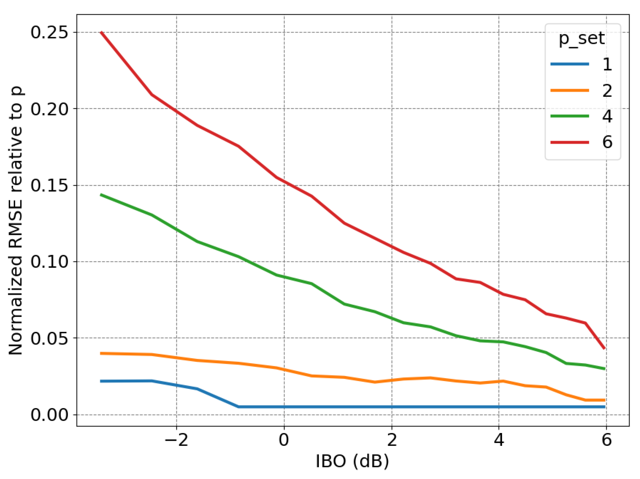
4.2. Accuracy of Rapp Model Parameter Estimation

While the synchronization accuracy has been confirmed in the above subsection, the accuracy of the whole framework in estimating nonlinearity model coefficients should be assessed. For the same parameters mentioned above, 300 random time offsets, Δ t 10 ; 10 (samples), and random frequency offsets, Δ f 3 ; 3 (subcarrier spacings), were generated while varying Rapp model parameters p and V sat . The Rapp model was iteratively obtained with initial vectors of tested p and V s a t values containing 50 equidistant samples in the ranges of < 0.1 , 20 > , and < max x n ^ 50 , max x n ^ > , respectively. The root mean squared errors of the estimates, normalized by real values, are presented in Figure 4 and Figure 5 for p and V sat , respectively. For easier interpretation, the V sat value is converted into IBO on the x-axis. In both cases, higher NRMSE is expected for very low IBO values. A very low IBO results in a significant part of the transmitted waveform being clipped, resulting in stronger distortion on the output. In such conditions, synchronization at the receiver performs worse, reducing estimation performance. However, by decreasing the PA input power (e.g., by introducing some additional attenuation), the IBO increases, allowing the PA to be characterized more accurately. For the case of an IBO equal to 4 dB for all the tested p-values, the estimation error is less than 10 % for p and less than 2 % for V sat . These estimates seem to be accurate enough to characterize the PA.
While the simulation allows for a fair comparison of the fitting performances in various conditions, the fitting accuracy can be slightly degraded in a real hardware setup. This can be caused mainly by some additional distortion sources of real hardware, e.g., white noise, the phase noise of oscillators, or the real PA not being perfectly matched with the selected PA model, e.g., revealing significant memory effects. While these will probably increase the MSE of the PA modeling, these are effects inherent to any PA measurement setup.

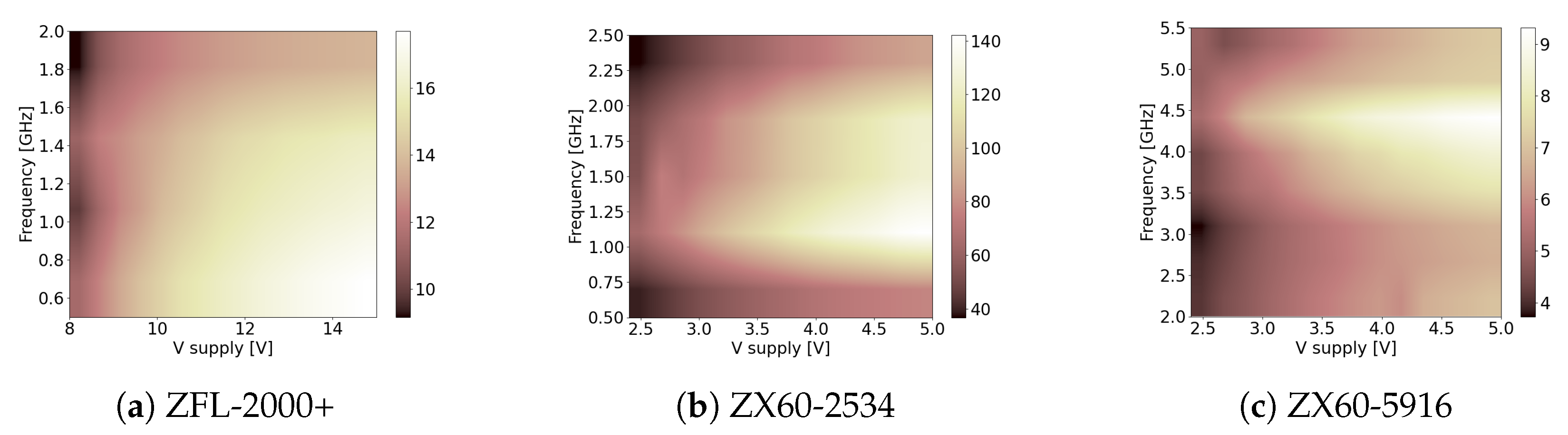
4.3. Measured PA Modeling

The polynomial approximation was computed for ν a = 5 using the pseudoinverse method described in Section 3.3. The Rapp model was estimated with the initial configuration as used in the previous subsection. Although the obtained measurement and modeling framework allows for estimating both AM/AM and AM/PM characteristics, only the first one, which has a more significant impact on transmitter performance degradation, is analyzed below.
Figure 6 presents examples of AM/AM characteristics obtained for all three tested PAs, along with Rapp models and polynomial models. It can be observed that both models accurately approximate the received signal in the low-amplitude region. However, for the higher input signal amplitudes, the polynomial model reveals a significant error. While increasing the polynomial order may potentially reduce this error, it would also lead to a significantly higher number of coefficients compared to the Rapp model, which utilizes only three parameters. On the other hand, the characteristics obtained from the Rapp model almost perfectly match the AM/AM samples across the entire range of input amplitudes. It can be concluded that the Rapp approximation is much more accurate for these amplifiers.
Although the Rapp model employs only three coefficients to describe the PA characteristics, it is relatively straightforward to analyze how these coefficients change with varying supply voltage and carrier frequency. The results for all input parameter values are presented as heatmaps in Figure 7, Figure 8 and Figure 9.
First, it can be observed that the gain for each PA increases with the supply voltage. Nevertheless, the rate of this increase is significantly different between frequencies. It is worth noting that in each scenario, there is a significant difference between the highest and the lowest values, equivalent to at least a two-fold difference. Recall that this represents a voltage gain in linear scale, equating to a power gain change of at least 6 dB. A similar analysis is observable when examining the variability of the PA smoothness factor, p, in Figure 8. For the ZFL-2000+ model, the nonlinear working range increases with the rise in both the supply voltage and frequency, expanding smoothly across input parameters. However, for the other two models, significant variability in the p-value is noticeable. Despite significant differences between the PAs, it is noteworthy that the maximum p-values for all cases do not exceed p = 3.0 . This implies that the examined amplifiers generally exhibit highly nonlinear behavior. Finally, the saturation voltage, V s a t , changes with the input parameters by at least two-fold for each PA, as shown in Figure 9. While in general, it is the lowest for a low supply voltage, its variability represents a non-trivial function of two input parameters.
The IQ samples as well as the obtained PA model parameters are available in reference [13].

5. Conclusions

This paper proposes a measurement and signal-processing framework for power amplifier nonlinearity characterization, enabling its utilization with generic IQ-based transmitters and receivers. Both simulations and real PA measurements confirm the sufficient accuracy of the proposed solution. Moreover, looking at the overall variability in the Rapp model parameters of the measured PAs, it is evident that their characteristics change significantly over the supply voltage and carrier frequency. Considering that next-generation wireless systems will operate over a wider carrier frequency range, possibly, with varying PA supply voltage to boost energy efficiency, the awareness of the PA nonlinear characteristics can be a crucial point in achieving the required quality of service (QoS) goals. The proposed PA nonlinearity characterization framework can be a useful tool to achieve this goal.
The next step in this research can be to extend the framework to characterize envelope-tracking amplifiers (of dynamically adjustable supply voltage) or real-time PA power consumption.

Author Contributions

Conceptualization, P.K.; methodology, P.K.; software, P.K. and K.K.; writing—original draft preparation, K.K.; writing—review and editing, P.K.; visualization, K.K.; supervision, P.K.; project administration, P.K.; funding acquisition, P.K. All authors have read and agreed to the published version of the manuscript.

Funding

This work was funded by the Polish National Science Centre, project no. 21/41/B/ST7/00136.

Data Availability Statement

The transmitted and received samples for all considered PAs are publicly available at https://doi.org/10.5281/zenodo.10519547 (accessed on 22 April 2024) along with the obtained PA models.

Conflicts of Interest

The authors declare no conflicts of interest.

Abbreviations

The following abbreviations are used in this manuscript:
PApower amplifier
VNAvector network analyzer
SDRsoftware-defined radio
SAspectrum analyzer
PAPRpeak-to-average power ratio
EEenergy efficiency
OFDM    orthogonal frequency division multiplexing
ETenvelope tracking
DPDdigital pre-distortion
WCDMAwideband code division multiple access
RFradio frequency
DUTdevice under test
DCdirect current
DACdigital-to-analog converter
ADCanalog-to-digital converter
DFTdiscrete Fourier transform
IDFTinverse discrete Fourier transform
AM/AMamplitude modulation to amplitude modulation
AM/PMamplitude modulation to phase modulation
IFintermediate frequency
QoSquality of service

References

  1. Thota, S.; Kamatham, Y.; Paidimarry, C.S. Analysis of hybrid PAPR reduction methods of OFDM signal for HPA models in wireless communications. IEEE Access 2020, 8, 22780–22791. [Google Scholar] [CrossRef]
  2. Wang, C.X.; You, X.; Gao, X.; Zhu, X.; Li, Z.; Zhang, C.; Wang, H.; Huang, Y.; Chen, Y.; Haas, H.; et al. On the road to 6G: Visions, requirements, key technologies and testbeds. IEEE Commun. Surv. Tutor. 2023, 25, 905–974. [Google Scholar] [CrossRef]
  3. Bossy, B.; Kryszkiewicz, P.; Bogucka, H. Energy-Efficient OFDM Radio Resource Allocation Optimization With Computational Awareness: A Survey. IEEE Access 2022, 10, 94100–94132. [Google Scholar] [CrossRef]
  4. Joung, J.; Ho, C.K.; Adachi, K.; Sun, S. A survey on power-amplifier-centric techniques for spectrum-and energy-efficient wireless communications. IEEE Commun. Surv. Tutor. 2014, 17, 315–333. [Google Scholar] [CrossRef]
  5. Tafuri, F.F.; Sira, D.; Nielsen, T.S.; Jensen, O.K.; Mikkelsen, J.H.; Larsen, T. Memory models for behavioral modeling and digital predistortion of envelope tracking power amplifiers. Microprocess. Microsyst. 2015, 39, 879–888. [Google Scholar] [CrossRef]
  6. Hoffmann, M.; Kryszkiewicz, P. Contextual Bandit-Based Amplifier IBO Optimization in Massive MIMO Network. IEEE Access 2023, 11, 127035–127042. [Google Scholar] [CrossRef]
  7. Ghannouchi, F.M.; Hammi, O. Behavioral modeling and predistortion. IEEE Microw. Mag. 2009, 10, 52–64. [Google Scholar] [CrossRef]
  8. Wisell, D. Measurement Techniques for Characterization of Power Amplifiers. Ph.D. Thesis, KTH, Stockholm, Sweden, 2007. [Google Scholar]
  9. Clark, C.J.; Silva, C.P.; Moulthrop, A.A.; Muha, M.S. Power-amplifier characterization using a two-tone measurement technique. IEEE Trans. Microw. Theory Tech. 2002, 50, 1590–1602. [Google Scholar] [CrossRef]
  10. Zhang, Y.; Guo, X.; He, Z.; Huang, H.; Huang, J.; Nie, M.; Wang, L.; Yang, A.; Lu, Z. Characterization for multiharmonic intermodulation nonlinearity of RF power amplifiers using a calibrated nonlinear vector network analyzer. IEEE Trans. Microw. Theory Tech. 2016, 64, 2912–2923. [Google Scholar] [CrossRef]
  11. Jeckeln, E.; Ghannouchi, F.; Sawan, M. A new adaptive predistortion technique using software-defined radio and DSP technologies suitable for base station 3G power amplifiers. IEEE Trans. Microw. Theory Tech. 2004, 52, 2139–2147. [Google Scholar] [CrossRef]
  12. Boumaiza, S.; Helaoui, M.; Hammi, O.; Liu, T.; Ghannouchi, F.M. Systematic and adaptive characterization approach for behavior modeling and correction of dynamic nonlinear transmitters. IEEE Trans. Instrum. Meas. 2007, 56, 2203–2211. [Google Scholar] [CrossRef]
  13. Kryszkiewicz, P.; Kostrzewska, K. Measurements of Nonlinearity Characteristics and Power Consumption of 3 Power Amplifiers (ZFL-2000+, ZX60-2534, ZX60-5916); CERN: Geneve, Switzerland, 2024. [Google Scholar] [CrossRef]
  14. Kryszkiewicz, P.; Kliks, A.; Bogucka, H. Obtaining low out-of-band emission level of an NC-OFDM waveform in the SDR platform. In Proceedings of the 2015 International Symposium on Wireless Communication Systems (ISWCS), Brussels, Belgium, 25–28 August 2015; pp. 66–70. [Google Scholar]
  15. Kryszkiewicz, P. Amplifier-coupled tone reservation for minimization of OFDM nonlinear distortion. IEEE Trans. Veh. Technol. 2018, 67, 4316–4324. [Google Scholar] [CrossRef]
  16. Rohde & Schawarz. FSL6 Manual. Available online: https://scdn.rohde-schwarz.com/ur/pws/dl_downloads/dl_common_library/dl_manuals/gb_1/f/sfl_1/FSL_OperatingManual_en_12.pdf (accessed on 22 April 2024).
  17. Newton, T. Channel Sounding in White Space Spectrum; Technical Report 1MA199; Rohde&Schwarz/Neul: Columbia, MD, USA, 2011. [Google Scholar]
  18. Georgiev, S.G.; Erhan, İ.M. LAGRANGE INTERPOLATION ON TIME SCALES. J. Appl. Anal. Comput. 2022, 12, 1294–1307. [Google Scholar] [CrossRef]
  19. Gharaibeh, K.M. Nonlinear Distortion in Wireless Systems: Modeling and Simulation with MATLAB; John Wiley & Sons: New York, NY, USA, 2011. [Google Scholar] [CrossRef]
  20. Nokia. Realistic Power Amplifier Model for the New Radio Evaluation; 3GPP doc. R4-163314; 3GPP: Sophia Antipolis, France, 2016. [Google Scholar]
  21. Glock, S.; Rascher, J.; Sogl, B.; Ussmueller, T.; Mueller, J.E.; Weigel, R. A Memoryless Semi-Physical Power Amplifier Behavioral Model Based on the Correlation Between AM–AM and AM–PM Distortions. IEEE Trans. Microw. Theory Tech. 2015, 63, 1826–1835. [Google Scholar] [CrossRef]
  22. Al-kanan, H.; Tafuri, F.; Li, F. Hysteresis nonlinearity modeling and linearization approach for Envelope Tracking Power Amplifiers in wireless systems. Microelectron. J. 2018, 82, 101–107. [Google Scholar] [CrossRef]
  23. Li, D.; Yu, H. A new model for envelope tracking power amplifier modeling and digital predistortion. In Proceedings of the 2016 8th International Conference on Wireless Communications & Signal Processing (WCSP), Yangzhou, China, 13–15 October 2016; pp. 1–5. [Google Scholar]
  24. Mengozzi, M.; Angelotti, A.M.; Gibiino, G.P.; Florian, C.; Santarelli, A. Joint dual-input digital predistortion of supply-modulated RF PA by surrogate-based multi-objective optimization. IEEE Trans. Microw. Theory Tech. 2021, 70, 35–49. [Google Scholar] [CrossRef]
  25. Press, W.H. Numerical Recipes, 3rd ed.; The Art of Scientific Computing; Cambridge University Press: Cambridge, UK, 2007. [Google Scholar]
  26. Golub, G.H.; Van Loan, C.F. Matrix Computations; JHU Press: Baltimore, MD, USA, 2013. [Google Scholar]
  27. Strang, G. Introduction to Linear Algebra; SIAM: Philadelphia, PA, USA, 2022. [Google Scholar]
  28. MATLAB, M. Compute Square Root Using CORDIC. Available online: https://www.mathworks.com/help/fixedpoint/ug/compute-square-root-using-cordic.html (accessed on 22 April 2024).
  29. Mini-Circuits. ZFL-2000+. Available online: https://www.minicircuits.com/pdfs/ZFL-2000+.pdf (accessed on 22 April 2024).
  30. Mini-Circuits. ZX60-5916. Available online: https://www.minicircuits.com/pdfs/ZX60-5916MA+.pdf (accessed on 22 April 2024).
  31. Mini-Circuits. ZX60-2534. Available online: https://www.minicircuits.com/pdfs/ZX60-2534MA+.pdf (accessed on 22 April 2024).
Figure 1. System model.
Electronics 13 01643 g001
Figure 2. Received signal correction—block diagram.
Electronics 13 01643 g002
Figure 3. Exemplary PA AM/AM characteristics before and after fine corrections.
Electronics 13 01643 g003
Figure 4. The root mean square error (RMSE) of the p estimation, normalized over the known p-value for varying p and V sat values averaged over 300 random time and frequency offsets.
Electronics 13 01643 g004
Figure 5. The root mean square error (RMSE) of the V sat estimation, normalized over the known V sat value for varying p and V sat values averaged over 300 random time and frequency offsets.
Electronics 13 01643 g005
Figure 6. Examples of AM/AM characteristics and models for all tested PAs. (a) Measurements and modeling for ZFL-2000+ at 2 GHz with 12 V supply. (b) Measurements and modeling for ZX60-2534 at 2 GHz with 4 V supply. (c) Measurements and modeling for ZX60-5916 at 2 GHz with 4 V supply.
Electronics 13 01643 g006
Figure 7. Estimated G as a function of varying supply voltage and carrier frequency.
Electronics 13 01643 g007
Figure 8. Estimated p as a function of varying supply voltage and carrier frequency.
Electronics 13 01643 g008
Figure 9. Estimated V s a t as a function of varying supply voltage and carrier frequency.
Electronics 13 01643 g009
Table 1. Supply voltage range and tested values for the PAs.
PA ModelVoltage RangeTested Voltages
ZFL-2000+max 17 V8.0, 9.5, …, 14.5, 15.0 V
ZX60-59162.8–5.0 V2.4, 2.6, …, 4.8, 5.0 V
ZX60-25342.8–5.0 V2.4, 2.6, …, 4.8, 5.0 V
Table 2. Frequency range and test frequencies for the tested PAs.
PA ModelFrequency RangeTested Frequencies
ZFL-2000+10–2000 MHz0.5, 1, …, 2 GHz
ZX60-59161500–6000 MHz2, 2.5, …, 5.5 GHz
ZX60-2534500–2500 MHz0.5, 1, …, 2.5 GHz
Table 3. Mean signal power on the PA input and maximum no-damage PA input power.
PA ModelMean Power
Pgen [dBm]
Max Input Power
P m a x i n [dBm]
ZFL-2000+−65
ZX60-5916010
ZX60-2534−26−15
Table 4. Correction program outcome.
Frequency Offsets [Subcarrier Spacing]
Set OffsetResultAbsolute Error
3.43.3960.004
9.59.4910.009
1.21.1980.002
6.36.2930.007
2.92.8960.004
4.44.3950.005
6.46.3930.007
5.15.0940.006
4.44.3950.005
5.15.0940.006
Time offsets [sample period]
Set offsetResultAbsolute Error
2.32.2970.003
6.36.2970.003
8.88.8030.003
8.08.0000.000
4.56.4990.001
2.62.6010.001
6.56.5000.000
4.94.9020.002
2.82.8030.003
4.84.8030.003
Disclaimer/Publisher’s Note: The statements, opinions and data contained in all publications are solely those of the individual author(s) and contributor(s) and not of MDPI and/or the editor(s). MDPI and/or the editor(s) disclaim responsibility for any injury to people or property resulting from any ideas, methods, instructions or products referred to in the content.

