Article

Graphical Design Approach for UWB Stacked CG LNA Using Inversion Coefficient

1
MEMS-Vision LLC, Cairo 11375, Egypt
2
Integrated Circuits Laboratory, ECE Department, Faculty of Engineering, Ain Shams University, Cairo 11566, Egypt
*
Authors to whom correspondence should be addressed.
Electronics 2024, 13(9), 1602; https://doi.org/10.3390/electronics13091602
Submission received: 2 March 2024 / Revised: 11 April 2024 / Accepted: 16 April 2024 / Published: 23 April 2024

Abstract

:
The design of ultra-wide-band (UWB) low-noise amplifiers (LNAs) entails a large number of design challenges and tradeoffs, which include sustaining good input matching over a wide bandwidth along with finding a proper compromise between various LNA performance metrics, such as gain, bandwidth, noise figure, power, and linearity. This paper presents a design approach for UWB LNAs based on the inversion coefficient (IC). The proposed approach is a graphical design approach where the proper operating point is chosen based on predefined constraints. A complete systematic solution is presented for the problem of UWB input matching with a high degree of analytical accuracy. The design approach is illustrated through the design of two UWB stacked common-gate LNAs in 65 nm technology. The post-layout simulation results show very good agreement with analytical expectations. The first LNA achieves an S 11 better than −8.2 dB over a 27.6 GHz frequency range, a gain of 12.4 dB over a 16.5 GHz bandwidth, a minimum noise-figure, NF, of 4.5 dB, and an I I P 3 of −5.2 dBm while consuming only 530 μ W. The second LNA achieves an S 11 better than −15 dB over an 8.8 GHz frequency range, a gain of 12.5 dB over a 6.8 GHz bandwidth, a minimum NF of 4 dB, and an I I P 3 of −4.3 dBm while consuming only 550 μ W.

1. Introduction

UWB communication has been a growing field of research since the Federal Communications Commission (FCC) changed its regulations to allow the unlicensed usage of UWB signals in 2002. UWB signals are defined by the FCC as those having −10 dB bandwidths greater than 500 MHz with a transmitted power mask limited to −41.3 dBm/MHz within the 3.1–10.6 GHz band [1]. The most popular implementation of UWB systems is the impulse radio technique (IR-UWB), where each symbol is represented by a short pulse of signal followed by a long time off with no power transmitted, thus saving power. This is the key difference between IR-UWB and NB communications, where for the latter, a modulated RF carrier is continuously transmitted throughout the whole symbol period [2]. The inherent power-saving property of the IR-UWB transceivers, along with their high data rate capability, make them an attractive choice for high-accuracy ultra-low-power wireless body area networks (WBANs) powered by a tiny battery or even an energy harvesting system [3]. Moreover, IR-UWB transceivers have become a strong candidate for indoor localization and ranging applications due to the utilization of very short data pulses. High-bandwidth, very short pulses are used to accurately estimate time of flight (TOF) and time of arrival (TOA) metrics, thus achieving high-precision ranging with minimal distance errors [4]. In addition, UWB technology has found its path towards other various applications, such as smart car keys, RFIDs, personal area networks (PANs), and even modern implementations of synthetic aperture radars (SARs).
One of the most vital building blocks of UWB systems is the LNA. The design of UWB LNAs entails a large number of challenges and trade-offs, such as maintaining good input matching over the wide amplifier bandwidth and achieving a high gain, low noise, and high I I P 3 while maintaining a compact area and low power dissipation. Achieving these seemingly contradictory specifications requires a lot of design iterations, which if not properly managed, may lead to suboptimal designs that limit the performance of the whole system. Thus, a systematic design approach is recommended in order to maximize the LNA figure of merit, F o M , and to understand the potential and limitations of different topologies and technology nodes while minimizing design time and effort. There are a lot of research efforts aiming to standardize the design process and offering different design methodologies. The work in [5] is an LNA design methodology where g m / I D is used as a benchmark for the transistor operating point. Device parameters are extracted by simulation in terms of g m / I D and represented as a table dataset or a lookup table (LUT). The specifications of the target circuit topology are then represented analytically in terms of the small-signal device parameters, where the optimum g m / I D is chosen to achieve pre-defined target specifications and optimize the circuit performance. The main drawback of this approach is that it requires the user to perform a full characterization of the MOSFET under all size and bias conditions to build LUTs for each device parameter. Another LUT-based methodology is found in [6], where the gate-source voltage is chosen to maximize linearity while the transistors’ widths are chosen to maximize other LNA specifications. This method also requires full MOSFET characterization prior to the design phase. The aforementioned limitations imply the need for a simple transistor device model that clearly describes transistor physics and accurately describes transistor parameters in all regions of interest (namely, weak inversion, moderate inversion, and strong inversion), and this is what the charge-based EKV model does [7]. The simplified EKV model in [7] represents the transistor operating region by the inversion coefficient term, I C , which is a normalization of the drain current I D to a technology parameter called the specific current I s p e c . The I C divides the transistor regions of operation depending on the level of channel inversion as follows:
I C < 0.1 : weak inversion ( WI ) 0.1 < I C < 10 : moderate inversion ( MI ) I C > 10 : strong inversion ( SI )
It is worth noting that having a design approach that considers weak inversion and moderate inversion in addition to strong inversion (rather than the square law that considers strong inversion only) is crucial, especially for designs conducted in modern advanced technologies, where technologies’ f t have risen considerably but the low-power standards, such as the Internet of Things’ (IoT) standards, still define relatively low carrier frequencies. In such cases, operating at weak or moderate inversions leads to low-power operation and can still satisfy the operating frequency.
The I C is adopted in [8,9] as the basis of their design methodology. The design methodology adopted in [8] starts by characterizing the MOSFET in the target technology to extract the technology parameters forming the device parameters’ expressions. This step is performed once for each technology. After that, a circuit analysis is performed to derive the design equations for the target topology. This step is unique and has to be performed for each circuit topology. The final step is to write a MATLAB script that optimizes the circuit equations based on a defined F o M to find the optimum biasing and sizing point. One main missed part in this methodology is that the choice of transistor lengths is made arbitrarily without specific reasoning behind it and thus is not optimized. A two-step approach is adopted in [9], namely active and passive, where the active step is used to meet the performance specifications and the passive step is used to meet the required matching. In the active step, the gain and the N F metrics are set as an initial condition, and then an optimum transistor bias point, I C o p t , at a fixed transistor width and length is found based on maximizing a pre-defined F o M . After that, a loop iterates on the sizing variables W and L until all performance specifications are achieved. In the passive step, input matching specifications are calculated in terms of the device passives, parasitic capacitances, and resistances. Then, a loop iterates on the circuit passives until the required matching is achieved. The automation script then tests again against performance specifications, and if they are met, the design is complete; if not, the whole process is repeated again. During the device parameter extraction step, the gate-source capacitance is assumed to be independent of the I C , which is not accurate due to the intrinsic part of it. This leads to inaccurate results, especially for matching metrics (passive step). The methodology in [10] adopts the Advanced Compact MOSFET model (ACM) for optimizing resistive-feedback LNAs and describes all the circuit equations in terms of seven transistor parameters. However, the assumption of too many arbitrarily chosen constraints using only one variable (IIP3) for optimization and suboptimal matching procedures necessitates a design loop of many iterations while reaching suboptimal design points and very small matching bandwidth.
The remaining part of this paper is organized as follows. Section 2 gives a glimpse into the design approach used. Section 3 describes the EKV charge-based transistor model used to describe transistor parameters. Section 4 presents the analysis of the LNA topology used in this paper, which is the stacked common-gate LNA. Section 5 describes the design flow and discusses the results. And finally, the work is concluded in Section 6.

2. Design Methodology

A UWB LNA design approach based on I C and LNA F o M is presented in this paper. As shown in Figure 1, the design approach consists of four main steps. First, all device parameters of interest are derived in terms of I C , W, and L, where W and L are the transistor channel width and length, respectively. The second step is to represent different performance metrics in terms of device parameters and hence in terms of I C , W, and L. The third step is to define the design constraints imposed on the design and define the F o M to be maximized in terms of I C , W, and L to generate the design graphs. The final step is to choose the proper bias point and sizing, I C o , W o , and L o , using the design graphs. So, basically, the optimization process is conducted graphically by selecting the most appropriate IC that satisfies all the design constraints and maximizes F o M .
It is worth noting that unlike the methodologies in [5,6], the adopted approach offers a complete analytical solution where every device parameter as well as the transistor biasing point and sizing can be predicted analytically. Moreover, the design steps do not require lengthy iterations and trials, like in the cases of [10] or [11]. The choice of the transistor length is made to maximize the input matching bandwidth, as discussed in Section 5, giving the proposed approach an edge on the one in [8]. A multi-variable F o M covering all the important circuit specifications is used for optimization rather than the use of only one variable, as in the case of [10]. Finally, both the intrinsic and extrinsic parts of the gate-source capacitance are modeled as outlined in Section 3, thus more accurate results for input matching are achieved in contrast to the methodology in [9].

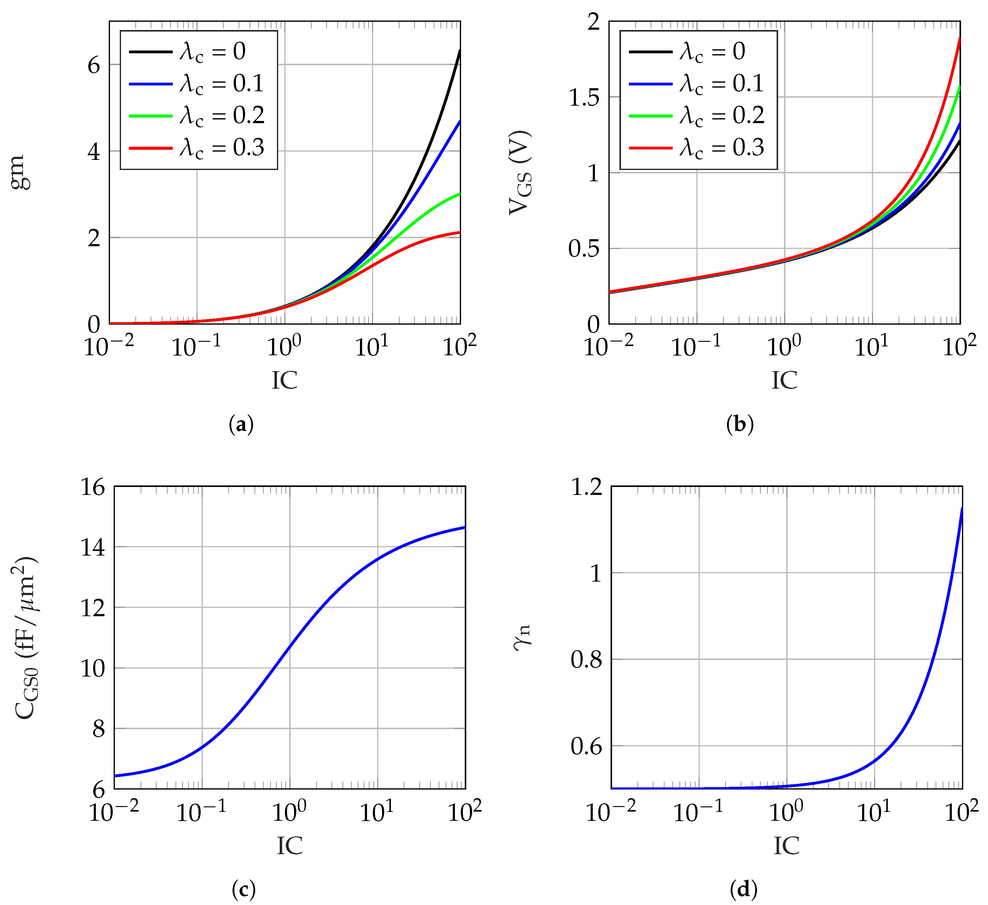
3. Charge-Based Transistor Model

The EKV charge-based model was first introduced by C. Enz, F. Krummenacher and E.A. Vittoz [8]. The transistor operating point is described in terms of the inversion coefficient,
I C = I D I s p e c ,
I s p e c = W L I s p e c ,
I s p e c = 2 n μ n C o x U T 2 ,
where I D is the transistor drain current, I s p e c is the transistor-specific current, I s p e c is the specific current per square, W is the transistor gate width, L is the transistor gate length, n is the nonideality factor, μ n is the low-field mobility, C o x is the oxide capacitance per unit area, and U T = K T q is the thermal voltage.
The inversion coefficient parameter can be related to the normalized channel charge using [12]:
I C i d s a t = q s 2 + q s q d s a t 2 q d s a t ,
q d s a t = λ c i d s a t 2 ,
where i d s a t is the normalized drain saturation current, q s is the normalized source charge, q d s a t is the normalized drain saturation charge, and λ c = L s a t L is the velocity saturation parameter, which represents the percentage of the channel length in which the carrier’s velocity is saturated. From (4) and (5), q s can be represented as [7]
q s = ( λ c I C + 1 ) 2 + 4 I C 1 2 ,
The normalized gate transconductance, g m , is expressed as [8]
g m = G m G s p e c = 1 n 2 q s λ c ( λ c I C + 1 ) + 2 ,
where G m is the transistor transconductance and G s p e c = I s p e c U T is the transconductance normalization factor.
Considering the gate-source voltage V G S , an analytical expression in terms of IC can be deduced from the general solution of the compact charge-based model found in [7]:
2 q i + l n ( q i ) = v p v ,
where q i , v, and v p are the normalized channel charge, normalized channel voltage, and normalized pinch-off voltage, respectively. At the source end of the channel, this becomes [7]
2 q s + l n ( q s ) = v p v s .
But, from [7],
v p = V p U T = V G V T 0 n U T ,
v s = V s U T ,
where V G and V T 0 are the transistor gate voltage and threshold voltage in equilibrium, respectively, where the latter is a technology parameter. Substituting (10) and (11) in (9)
V G n V s V T 0 n U T = 2 q s + l n ( q s ) .
Assuming zero source voltage ( V s = 0 ),
V G S = V T 0 + n U T ( 2 q s + l n ( q s ) ) .
For a non-zero bulk-source voltage ( V B S > 0 ), an additional term is added to (13) to model the body effect.
The gate-source capacitance per unit area, C G S 0 is expressed in terms of IC using the following relations [13]:
C G S 0 = X 1 + X 2 C i n t 0 ,
C i n t 0 = n ( 1 + x ) / 3 n ,
x = ( I C + 0.25 + 0.5 ) + 1 ( I C + 0.25 + 0.5 ) 2 ,
where X 1 and X 2 are technology-dependent constants.
The gate-drain capacitance, C G D is expressed as
C G D = W C G D 0 ,
where W is the transistor width and C G D 0 is a technology-dependent parameter.
The thermal excess noise factor γ n is also a function of I C , where
γ n = γ w + α n I C ,
where γ w and α n are the weak inversion values of γ n and the inversion level dependency factor, respectively. Both are technology-dependent parameters.
The aforementioned device parameters ( g m , V G S , C G S , and γ n ) are plotted in Figure 2 against I C , with g m and V G S shown for different λ c values for 65 nm technology. According to [8], velocity saturation has a minor effect at lengths greater than or equal to 200 nm and can be neglected even for shorter lengths without much effect on the results’ accuracy, knowing that at lengths as small as 65 nm, λ c is about 0.3. The target application in this paper is the UWB LNA operating at frequencies of up to 10.6 GHz, while this technology’s f t is 200 GHz; thus, there is no need to utilize small transistor lengths and compromise the transistor gain and drain-source isolation. Also, as will be shown later, the moderate inversion region always offers the best compromise for the transistor bias point that maximizes the circuit F o M while achieving the design constraints. For all these reasons, λ c will be neglected in all the forthcoming analyses.
The accurate extraction of the model parameters is a very important step for accurate analytical predictions. This task has to be performed once for every technology node in order to be able to use the model. There has already been extensive research conducted in this domain, as can be found in [14], where the bottom line in the extraction process is performing curve-fitting to simulation data. This was performed in this work for the TSMC 65 nm process using DC and noise characterization for the NMOS and PMOS transistors by fitting the simulation data.
Table 1 summarizes the different model parameters for NMOS and PMOS transistors in the adopted technology. Simulation data for G m , V G S , C G S , C G D , and the output noise current are used for the proper extraction of the addressed model parameters.

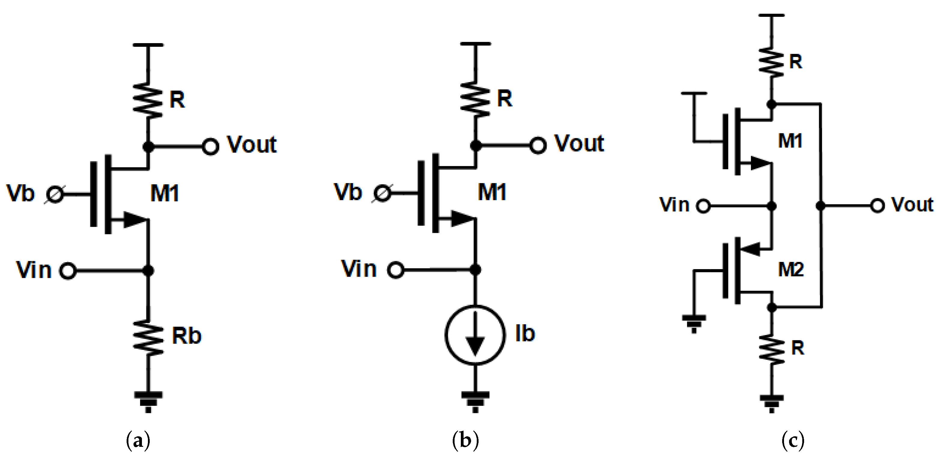
4. Analysis of the Stacked CG Topology

The stacked common-gate amplifier topology (Figure 3) is adopted for the UWB LNA of this work. In the stacked common-gate amplifier, the supply current is reused such that both the NMOS and the PMOS transistors act as active devices to boost the amplifier’s total transconductance ( G m t o t ). The main advantage of the stacked common-gate over the standard common-gate topology is that the former uses the available headroom more efficiently. As demonstrated in Figure 4, the stacked common-gate actively uses the headroom that is normally used on the biasing device in the standard common-gate.

4.1. PMOS-to-NMOS Sizing Ratio

The total transconductance of the amplifier equals the summation of NMOS and PMOS transconductances, G m n and G m p , respectively; however, for the same current, there are endless combinations of G m n and G m p that are determined by the PMOS to NMOS sizing ratio ( W L ) p ( W L ) n , which is equal to W p W n , assuming equal transistor lengths. Finding the sizing ratio ( W p W n ) that maximizes G m t o t is crucial for obtaining a better design. Neglecting the λ c -parameter, the overdrive voltages and transconductances of NMOS and PMOS transistors can be written as (ignoring body effect)
V o d n , p = n U T [ 2 q s n , p + l n ( q s n , p ) ] ,
G m n , p = I s p e c n , p q s n , p n U T ,
where
q s n , p = 4 I C n , p + 1 1 2 ,
where V o d , G m , and q s are the overdrive voltage, the transconductance, and the normalized channel charge at the source end of the transistor, respectively. Assuming that V o d n + V o d p = V , where V = V D D ( V T 0 n + V T 0 p ) , where the body effect is neglected for simplicity and without much effect on the results’ accuracy, this can be restated as follows:
V o d n + V o d p = X V + ( 1 X ) V = V ,
where X is the ratio of V o d n to the voltage headroom V and its value ranges from 0 to 1. Knowing that
G m t o t = G m n + G m p ,
the set of equations from Equation (19) through to Equation (22) have to be solved analytically. However, no closed-form expression can be obtained because these equations cannot be solved analytically, thus an approximation has to be made in order to find an analytical solution.

4.1.1. Strong Inversion Approximation

In strong inversion, I C 10 , thus q s n , p I C n , p , and as a result, Equation (19) can be approximated to
V o d n , p = 2 n U T I C n , p ,
G m n , p = I s p e c n , p I C n , p n U T .
From (23a) and the definition of X,
V o d n V o d p = I C n I C p = ( X 1 X ) .
But from (1) and due to current reuse,
I C n I C p = I s p e c p I s p e c n = ( X 1 X ) 2 ,
This can be rewritten as follows:
I C n = X 2 I C ,
I C p = ( 1 X ) 2 I C ,
I s p e c n = ( 1 X ) 2 I s p e c ,
I s p e c p = X 2 I s p e c ,
where I C and I s p e c are arbitrary constants. Substituting (23b) and (26) in (22)
G m t o t = I s p e c I C n U T [ ( 1 X ) 2 X + X 2 ( 1 X ) ] .
To find X for maximum G m t o t , then
G m t o t X = I s p e c I C n U T [ 1 2 X ] = 0 .
Equation (28) yields X = 0.5 . This result along with (1), (2), (19), and (26) yield
V o d n = V o d p = V o d ,
I C n = I C p = I C ,
I s p e c n = I s p e c p = I s p e c ,
G m n = G m p = G m ,
W p W n = I s p e c n I s p e c p ,

4.1.2. Weak Inversion Approximation

In weak inversion, I C 0.1 , thus (19) can be approximated to
V o d n , p = n U T l n ( q s n , p ) ,
G m n , p = I s p e c n , p q s n , p 2 n U T .
From (30a) and the definition of X,
q s n = e x p X V n U T ,
q s p = e x p ( 1 X ) V n U T .
From (20) and (31),
I C n = e x p 2 X V n U T + e x p X V n U T ,
I C p = e x p 2 ( 1 X ) V n U T + e x p ( 1 X ) V n U T ,
But, due to current reuse and from (1), I s p e c n I s p e c p = I C p I C n , thus
I s p e c n = I s p e c I C p ,
I s p e c p = I s p e c I C n ,
where I s p e c is an arbitrary constant. Substituting (30b), (31), (32), and (33) in (22)
G m t o t = I s p e c n U T f ( X ) ,
where
f ( X ) = [ e x p ( 2 X ) V n U T + e x p ( 1 + X ) V n U T + 2 e x p V n U T ] .
To find X for maximum G m t o t ,
G m t o t X = I s p e c V ( n U T ) 2 [ e x p ( 1 + X ) V n U T e x p ( 2 X ) V n U T ] = 0 ,
hence X = 0.5 . This makes (29) also valid in weak inversion.
Therefore, it can be concluded that for the maximum G m t o t for stacked PMOS and NMOS transistors, a ( W L ) p to ( W L ) n ratio should be chosen such that V x = 1 2 ( V D D V T n V T p ) + V T p = V D D 2 V T n 2 + V T p 2 .

4.2. Input Matching

The input impedance of the stacked common-gate stage can be deduced from the small signal model shown in Figure 5, where the AC coupling capacitance C 1 in Figure 3 is selected to be effectively a short circuit in the mid-band frequency range of interest.
Z i n ( s ) = R i n + s L p + s 2 L p R i n C i n 1 + s R i n C i n ,
where R i n ( R i n = R 2 + r o 2 1 + 2 G m r o 2 1 2 G m for R < < r o , where r o is the transistor output impedance) is the mid-band input impedance, L p is the bond wire inductance, and C i n = C G S n + C G S p + C S B n + C S B p C G S n + C G S p . This result is accurate for frequencies far greater than the C 1 corner frequency. Computing S 11 ,
S 11 ( ω ) = Z i n ( ω ) R s Z i n ( ω ) + R s ,
| S 11 ( ω ) | d B = 10 l o g [ ( R i n R s ) ω 2 L p τ i n ] 2 + ω 2 ( L p R s τ i n ) 2 [ ( R i n + R s ) ω 2 L p τ i n ] 2 + ω 2 ( L p + R s τ i n ) 2 ,
where τ i n = R i n C i n .

4.3. Gain

From Figure 4c, the amplifier voltage gain at the mid-band frequency range can be formulated as
A v = V o u t V x = ( 1 + 2 G m r o 2 ) R 2 r o 2 + R 2 G m R ,
for R < < r o and G m r o > > 1 . These assumptions become inaccurate if the minimum feature length is used or at large currents; both extremes are avoided so as not to deteriorate amplifier gain or power consumption.

4.4. Bandwidth

The low-frequency corner of the signal bandwidth is determined by the AC coupling corner frequency as
f l o w = 1 2 π ( R s + R i n ) C 1 ,
while the high-frequency corner is determined by the output pole and can be expressed as
f h i g h = 1 π R C L ,
where the output impedance is equal to R 2 , C L = C G D n + C G D p + C D B n + C D B p C G D n + C G D p . f l o w is typically in the range of a few hundred megahertz for an AC coupling cap in the range of a few picofarads, where f h i g h is in the range of a few to tens of gigahertz, thus f h i g h can be considered the amplifier bandwidth.

4.5. Noise

There are three sources of noise in the circuit in Figure 3, namely M n , M p , and R, where, at the mid-band and high frequency, the first two can be lumped into one device with double the transconductance, as shown in Figure 6. From Figure 6, it can be shown that the gain from the combined transistor gate to the output is
| A v n | = G m R 1 + 2 G m R s .
Also, the signal gain (Figure 3) is
| A v , 0 | = V o u t V i n = R i n R s + R i n G m R = G m R 1 + 2 G m R s .
The generated output noise power from the lumped transistor and the output resistors have the following power densities:
V n , o u t , M n , p 2 ¯ = 4 K T γ 2 G m G m 2 R 2 ( 1 + 2 G m R s ) 2 = 2 K T γ G m R 2 ( 1 + 2 G m R s ) 2 ,
V n , o u t , R 2 ¯ = 4 K T R 2 = 2 K T R ,
where γ = ( γ n + γ p ) 2 is the average noise excess factor for NMOS and PMOS transistors, K is the Boltzmann constant, and T is the absolute temperature in Kelvin. The noise figure of the circuit can be deduced from (43) and (45) and is equal to
N F = 1 + V n , o u t , M n , p 2 ¯ + V n , o u t , R 2 ¯ 4 K T R s A v , 0 2 ,
N F = 1 + G m R γ + ( 1 + 2 G m R s ) 2 2 G m 2 R s R ,
N F e x c e s s = G m R γ + ( 1 + 2 G m R s ) 2 2 G m 2 R s R ,
where N F e x c e s s is the excess noise figure.

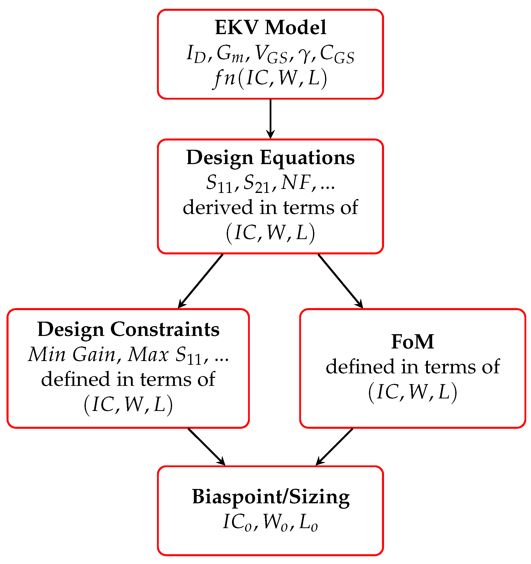
5. Graph-Based Design

The previous two sections represent the first two steps in the design approach, where the MOSFET parameters were defined in terms of the EKV model parameters and the circuit performance metrics were defined in terms of the MOSFET parameters. In this section, the remaining two steps are performed to complete the LNA design. The third step entails defining the design constraints that have to be met and the F o M to be maximized. Finally, the last step entails a bias point and size selection based on the data from the preceding step.

5.1. Design Constraints

The following constraints are used in this context; however, any other set of constraints can be used to fit other applications.

5.1.1. Minimum Gain Constraint

The LNA gain is one of its most critical performance metrics, thus it is reasonable to put a constraint on it
A v A m i n ,
where A m i n is the minimum gain constraint. From (40), it follows that
R A m i n / G m ,

5.1.2. Maximum N F Constraint

The N F is one of the crucial LNA performance metrics. A constraint on it can be driven as follows:
N F N F m a x ,
where N F m a x is the maximum N F constraint. From (46b), it follows that
R ( 1 + 2 G m R s ) 2 ( 2 N F m a x G m R s γ ) G m ,

5.1.3. Input Matching Constraint

This imposes a constraint on the max S 11 value and a constraint on input capacitance, C i n , which maximizes the S 11 bandwidth within which this value is not exceeded. The low-frequency S 11 value can be deduced from (39) by substituting ω with zero; this leads to
S 11 , l o w f r e q = 20 l o g | R i n R s R i n + R s | .
By targeting an S 11 ( S 11 , t a r g ) that is lower than S 11 , l o w f r e q ( S 11 , t a r g S 11 , l o w f r e q ) and re-arranging it, it imposes a constraint on R i n
1 10 S 11 , t a r g 20 1 + 10 S 11 , t a r g 20 R s R i n 1 + 10 S 11 , t a r g 20 1 10 S 11 , t a r g 20 R s .
By performing Equations (39) to (51), the frequency value at which S 11 is equal to its low-frequency counterpart, S 11 , l o w f r e q , is computed to be
ω S 11 = L p ( 2 R i n 2 C i n L p ) R s 2 R i n 2 C i n 2 L p 2 R i n 2 C i n 2 .
Hence, ω S 11 represents the bandwidth where S 11 is lower than its low-frequency value. For a certain R i n value and parasitic inductance value L p , C i n is the only degree of freedom to set the S 11 bandwidth. The C i n value that achieves the highest possible ω S 11 can be computed by taking the derivative of (53) with respect to C i n and equating the result to zero. This gives the C i n value that maximizes the S 11 bandwidth,
C i n , o = L p / R i n 2 .
This result is generic and can be applied to any LNA circuit that can be described using the small signal model in Figure 5.
The S 11 values derived in (39) and (51) neglect the AC coupling cap, C 1 , effect. As shown in Figure 7, adding C 1 raises the DC value of S 11 to 0 dB while the two curves (the actual S 11 curve and the simplified S 11 curve without C 1 ) approach each other at higher frequencies.

5.1.4. Headroom Constraint

This constraint is used to guarantee that the transistors are well into saturation and avoid operating near the triode region, deteriorating linearity. To achieve this, the maximum headroom on any of the output resistors is set by
H R = I D R V D D H R m a x ,
H R = I s p e c n I C R V D D H R m a x ,
where I D is the transistors’ drain current, V D D is the supply voltage, and H R m a x is the maximum allowable headroom on one resistor.
An extra constraint for the accuracy of the design flow and to avoid the short channel issues discussed before is the minimum transistor channel length allowed.

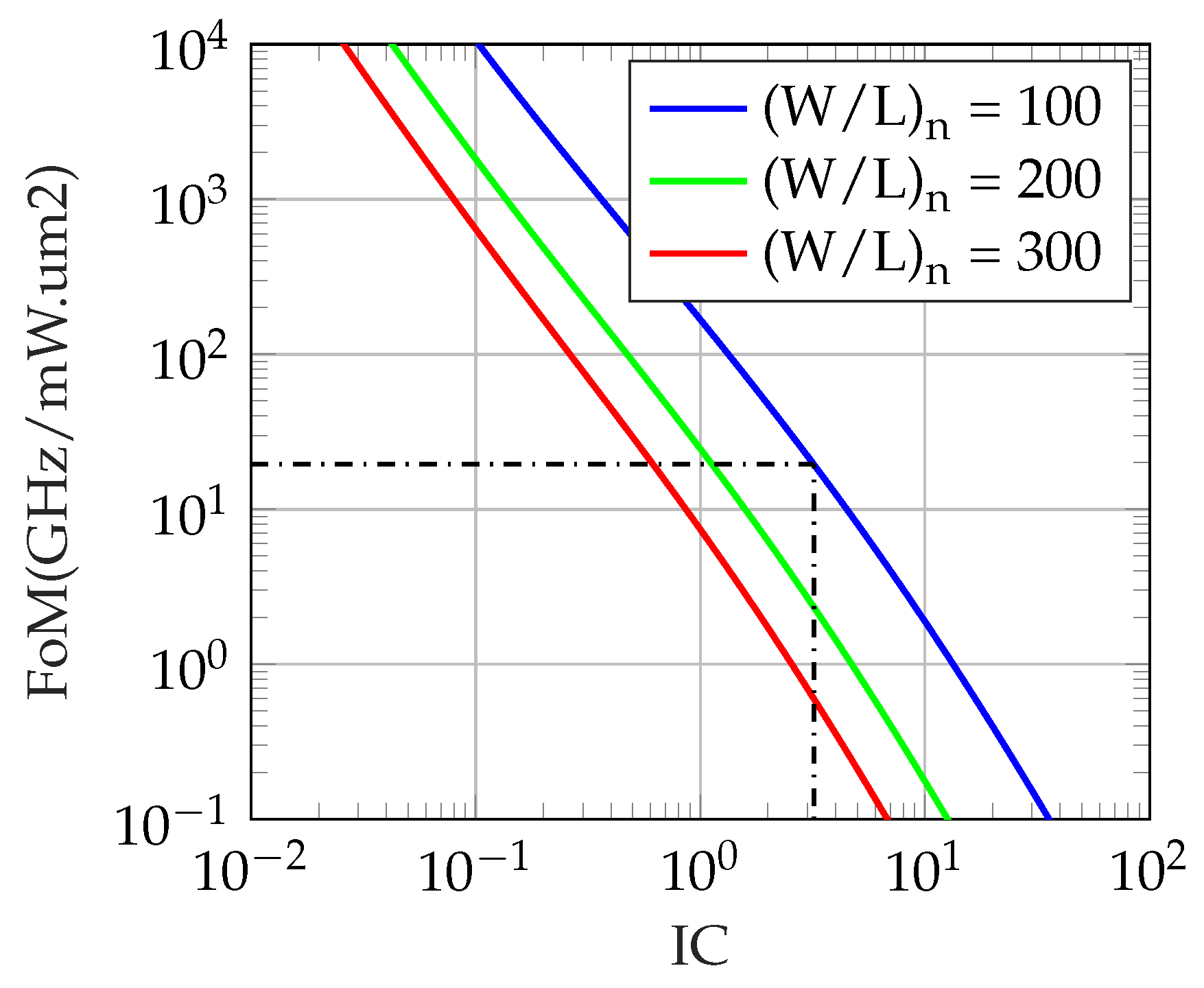
5.2. Figure of Merit

Defining the F o M for the LNA is the core of the design process. An adopted F o M has to be balanced and take all the important LNA specifications into consideration while targeting UWB applications. There are multiple F o M s reported in the literature, and the one in [15] is considered to be the most basic,
F o M 1 = A v · B W ( GHz ) N F e x c e s s · P D ( mW ) ( GHz / mW ) ,
where P D is the power dissipation in mW.
Adding the circuit area to the F o M is crucial for the LNA design; thus, the adopted F o M in this work is extended to F o M 1 by adding the transistor area in μ m 2 to minimize the total circuit area [16].
F o M 2 = A v · B W ( GHz ) N F e x c e s s · P D ( mW ) · A r e a ( μ m 2 ) ( GHz mW · μ m 2 ) ,

5.3. Sizing/Bias Point Selection

The last step in the design process is to choose the I C for the transistors and their sizing ( W L ) that meet all the design constraints and offer the best F o M for the circuit. This last step is demonstrated through two different designs: the design of a high-bandwidth LNA with a target gain and the design of a low-noise LNA.

5.3.1. High-Bandwidth LNA

Table 2 summarizes the design inputs and constraints used for the design. The I C and ( W L ) can be chosen graphically by plotting both the design parameters and the F o M . Figure 8 shows these parameters versus the I C , while Figure 9 shows the F o M for different ( W L ) n values, where ( W L ) p can then be deduced using (29e). The parameters in Figure 8 along with the F o M in Figure 9 are uniquely used for the choice of the transistors’ I C and the NMOS aspect ratio ( W L ) n . The first parameter is R i n , which is computed using R i n = 1 2 G m , where G m is given by (19b) and (20). The minimum and maximum constraints on R i n are given by the relation in (52). The second parameter is the transistors’ lengths, which satisfies the relation L = C G S n W n C G S 0 , where C G S n = C i n ( 1 + W p W n ) , C i n is set as in (54), and C G S 0 is given by (14), (15), and (16). The third parameter is the H R m a x , which can be computed from (55) while substituting R in (48). The fourth parameter is the bandwidth found in (42).
As noticed from Figure 8 and Figure 9, the I C that fulfills all the design constraints and achieves the best F o M is 3.2, which corresponds to the transistors’ operation in moderate inversion with a ( W L ) n of 100. This corresponds to a F o M of 19.6 GHz mW · μ m 2 , an L of 105 nm, a headroom of 28.9%, and a low-frequency input impedance of 95.4 Ω , which lies between the minimum value and the maximum value needed for a low-frequency S 11 of less than −10 dB, as stated in (52). The next step is to find the values of the load resistor, R, and the supply voltage, V D D , that correspond to an I C equal to 3.2. The load resistor value can be found by substituting A m i n in (48) with 3.17 (equivalent to 10 dB), while the G m can be computed from (19b) and (20) using an I C equal to 3.2 and a ( W L ) n equal to 100. The resultant R value is about 605 Ω . The supply voltage, V D D , can be computed from the equation V D D = V T 0 n + V T 0 p + 2 V o d , assuming no body effect, and the source and the bulk of each transistor are tied together, where V o d corresponds to the NMOS or the PMOS overdrive voltage, as deduced in (29a), which can be computed using (19a). The resultant V D D value is around 1 V. All the circuit performance parameters can also be calculated using the relationships deduced in Section 4 and Section 5. An actual circuit is built and verified using the TSMC 65 nm process based on the design outputs. In the first iteration of the design, the transistors’ bulk and source terminals are tied together, and the body effect is ignored. The body effect is considered afterwards (transistors’ bulks are tied to supply rails). The higher resulting transistor threshold voltages impose a higher supply voltage at the same I C . The physical layout of this LNA is shown in Figure 10. The shown layout was used in the post-layout simulations to examine the effect of added parasitics on the LNA performance, as reported in Table 3.
Figure 11 shows the results of the high-bandwidth LNA, and Figure 11a shows the S 21 across frequencies, and the low-frequency and high-frequency 3 dB corners are 50 MHz and 25.6 GHz, respectively, where the high-frequency corner reduces to 16.5 GHz post-layout. As shown in Figure 11b, the S 11 schematic simulation result is better than −8.6 dB across the frequency range of 0.6 GHz to 27.8 GHz, and the post-layout value is better than −8.2 dB across the frequency range of 0.7 GHz to 28.3 GHz. The N F is shown in Figure 11c, where it ranges from 4.3 dB to 11.8 dB for schematic simulations. The N F value is confined between 4.3 dB and 6 dB for the major portion of the frequency range; however, it deteriorates at very low frequencies, where the matching behavior is not ideal due to the DC-blocking cap effect. The N F post-layout result is more similar in ranges from 4.5 dB to 11.6 dB, and when it is confined between 4.5 dB and 5.8 dB for most of the spectrum.

5.3.2. Low-Noise LNA

Table 4 summarizes the design inputs and constraints used for the design. A similar approach is adopted in the design process as in the first LNA, but with different design constraints. Figure 12 shows the design parameters versus the I C , while Figure 13 shows the F o M for different ( W L ) n values. As noticed from Figure 12 and Figure 13, the I C that fulfills all the design constraints and achieves the best F o M is 0.9, which corresponds to the transistors’ operation in moderate inversion with a ( W L ) n of 450. This corresponds to a F o M of 3.1 GHz mW · μ m 2 , an L of 102 nm, a headroom of 29.9%, a gain ( A v ) of 12 dB, and a low-frequency input impedance ( R i n ) of 50 Ω , which lies between the minimum value and the maximum value needed for a low-frequency S 11 of less than −15 dB, as stated in (52). The next step is to find the values of the load resistor, R, and the supply voltage, V D D , that correspond to an I C equal to 0.9. The load resistor value can be found by substituting N F m a x in (50) with 2.51 (equivalent to 4 dB), while G m can be computed from (19b) using an I C equal to 0.9 and ( W L ) n equal to 450. The resultant R value is about 400 Ω . The supply voltage, V D D , can be computed from the equation V D D = V T 0 n + V T 0 p + 2 V o d , assuming no body effect, and the source and the bulk of each transistor are tied together, where V o d corresponds to the NMOS or the PMOS overdrive voltage, as deduced in (29a), which can be computed using (19a). The resultant V D D value is around 0.82 V. An actual circuit is built and verified using the TSMC 65 nm process based on the design outputs, and the results are summarized in Table 5. Figure 14 shows the physical layout of this LNA.
Figure 15 shows the results of the low-noise LNA, and Figure 15a shows the S 21 across frequencies, and the low-frequency and high-frequency 3 dB corners are 80 MHz and 9.9 GHz, respectively, and the high-frequency corner reduces to 6.9 GHz post-layout. As shown in Figure 15b, the S 11 schematic simulation result is better than −13 dB across the frequency range of 0.35 MHz to 9.9 GHz, and the post-layout value is better than −15 dB across the frequency range of 0.47 MHz to 9.2 GHz. The N F is shown in Figure 15c, and it ranges from 3.7 dB to 9.2 dB. The N F value is confined between 3.7 dB and 7 dB for the major portion of the frequency range; however, it deteriorates at very low frequencies. The N F post-layout result ranges from 4 dB to 9.3 dB and is confined between 4 dB and 7 dB for most of the spectrum.
The implemented circuits are compared with the state-of-the-art designs, as shown in Table 6, where the F o M used for the comparison is F o M = A v · B W ( GHz ) · I I P 3 ( mW ) N F e x c e s s · P D ( mW ) , which considers I I P 3 . The voltage gain and noise figure used in the F o M are the maximum and minimum across the frequencies, respectively. The implemented LNAs achieve better performance than most of the state-of-the-art designs. Exceptions to this are the designs in [8,10,17], which achieve better F o M . The high F o M of the LNA in [8] is possible due to the exceptional linearity of its design. However, this is achieved by utilizing a negative feedback loop, which increases design complexity and raises stability concerns. The matching bandwidth of the design in [10] is too small compared to the 3 dB bandwidth of the gain; thus, the real bandwidth is smaller than the reported one, deteriorating the achieved F o M . The LNA in [17] achieves a very wide bandwidth but at the cost of a higher power. Special techniques are used for noise and nonlinearity cancelation that result in increased complexity. Moreover, the very high power consumption makes the design unpreferable for use in low-power IoT applications. In [15], a three-stage amplifier with a second-order resonance circuit is used for controlled matching performance. This comes at the cost of relatively high power consumption and deteriorated linearity, thus compromising its F o M . The LNA in [18] utilizes an active notch filter for blocker suppression and linearity enhancement. The overall design uses a large number of bulky passives and multiple-stage topology compromising its area and power. The enhanced noise performance is a result of using a load resonant tank circuit. This is opposed to the use of two load resistors in our current reuse design to avoid the use of bulky inductors. The use of a feedback loop for input matching enhancement and a feedforward path for noise cancelation in the design in [19] results in an overall high power dissipation while not reducing the N F much. Multiple feedforward noise-canceling paths are used in [20] that result in low N F . However, the achieved bandwidth is relatively low due to the use of three transistors and an inductor in the output branch, increasing the parasitic capacitance at the output node. Finally, the use of a two-stage inverter-based amplifier in [21] increases the power consumption, significantly deteriorating the overall F o M despite achieving good linearity and noise performance.
It is worth noting that the objective of this work is not to report the best F o M but to present a graphical design approach that is guided by pre-defined constraints. Also, the comparison table with the state-of-the-art is intended only to show how the obtained performance by simulations fits with respect to previous work. However, it is understood that a real comparison can only be made if the design is fabricated and measured on silicon. In general, to increase the chances that simulations match the measurements after fabrication, all parasitics need to be included in simulations (which was performed in this work). However, it is understood that fabrications and measurements should still be conducted to validate that the inclusion of parasitics was conducted properly in the design phase. Nevertheless, this is beyond the objectives of this work.

6. Conclusions

A design approach for a UWB LNA based on an I C is proposed. The proposed approach is not limited to the transistor-strong inversion region, as in the case of adopting the square law. The design approach utilizes the EKV model to derive expressions for different circuit performance metrics as a function of transistor parameters. Since the EKV model is valid in weak, moderate, and strong inversion, the derived expressions can be used to choose the bias point of the circuit transistors while navigating through different operation regions. A number of design constraints are defined to set boundries to the design space, and the value of I C is used as a knob to maximize the F o M that combines relevant performance metrics. The design approach is applied to the design of two UWB stacked common-gate LNAs, and the design values and specifications obtained from the design approach were compared to simulation results, showing high agreement, indicating the effectiveness of the approach in reaching the target specifications with no iterations.
The designed high-bandwidth LNA achieves S 11 better than −8.2 dB over a 27.6 GHz frequency range, a gain of 12.4 dB over a 16.5 GHz bandwidth, a minimum NF of 4.5 dB, and an I I P 3 of −5.2 dBm while consuming only 530 μ W. The designed low-noise LNA achieves a S 11 of better than −15 dB over an 8.8 GHz frequency range, a gain of 12.5 dB over a 6.8 GHz bandwidth, a minimum NF of 4 dB, and an I I P 3 of −4.3 dBm while consuming only 550 μ W.

Author Contributions

Conceptualization, A.H. and A.I.; methodology, A.H.; validation, A.H.; formal analysis, A.H.; investigation, A.H.; resources, A.H.; data curation, A.H.; writing—original draft preparation, A.H.; writing—review and editing, A.I.; visualization, A.H.; supervision, A.I. All authors have read and agreed to the published version of the manuscript.

Funding

This research received no external funding.

Data Availability Statement

Simulation results and scripts are archived on the machines of the integrated circuits lab, ECE Dept, Faculty of Engineering, Ain Shams University, Cairo, Egypt.

Conflicts of Interest

Author Ahmed Hamed was employed by the company MEMS-Vision LLC. The remaining authors declare that the research was conducted in the absence of any commercial or financial relationships that could be construed as a potential conflict of interest.

Abbreviations

The following abbreviations are used in this manuscript:
ACMAdvanced Compact MOSFET
BWBandwidth
FCCFederal Communications Commission
ICInversion Coefficient
IoTInternet of Things
IRImpulse radio
LNALow-noise amplifier
LUTLookup table
MOSFETMetal–oxide–semiconductor field-effect transistor
NFNoise figure
PANPersonal area network
SARSynthetic aperture radar
TOATime of arrival
TOFTime of flight
UWBUltra-wide band
WBANWireless body area network

References

  1. Chandrakasan, A.; Lee, F.; Wentzloff, D.; Sze, V.; Ginsburg, B.; Mercier, P.; Daly, D.; Blazquez, R. Low-Power Impulse UWB Architectures and Circuits. Proc. IEEE 2009, 97, 332–352. [Google Scholar] [CrossRef]
  2. Vigraham, B.; Kinget, P.R. A Self-Duty-Cycled and Synchronized UWB Pulse-Radio Receiver SoC with Automatic Threshold-Recovery Based Demodulation. IEEE J. Solid-State Circuits 2014, 49, 581–594. [Google Scholar] [CrossRef]
  3. Gao, Y.; Zheng, Y.; Diao, S.; Toh, W.; Ang, C.; Je, M.; Heng, C. Low-Power Ultrawideband Wireless Telemetry Transceiver for Medical Sensor Applications. IEEE Trans. Biomed. Eng. 2011, 58, 768–772. [Google Scholar] [CrossRef] [PubMed]
  4. Gezici, S.; Tian, Z.; Giannakis, G.; Kobayashi, H.; Molisch, A.; Poor, H.; Sahinoglu, Z. Localization via ultra-wideband radios: A look at positioning aspects for future sensor networks. IEEE Signal Process. Mag. 2005, 22, 70–84. [Google Scholar] [CrossRef]
  5. Liu, J.; Lauga-Larroze, E.; Subias, S.; Fournier, J.; Bourdel, S.; Galup, C.; Hameau, F. A Methodology for the Design of Capacitive Feedback LNAs based on the gm/ID Characteristic. In Proceedings of the 2018 16th IEEE International New Circuits And Systems Conference (NEWCAS), Montreal, QC, Canada, 24–27 June 2018; pp. 178–181. [Google Scholar]
  6. Martinez-Perez, A.D.; Aznar, F.; Flandre, D.; Celma, S. Design-Window Methodology for Inductorless Noise-Cancelling CMOS LNAs. IEEE Access 2022, 10, 29482–29492. [Google Scholar] [CrossRef]
  7. Enz, C.; Vittoz, E. Charge-Based MOS Transistor Modeling; John Wiley & Sons: Hoboken, NJ, USA, 2006. [Google Scholar]
  8. Guitton, G.; Souza, M.; Mariano, A.; Taris, T. Design Methodology Based on the Inversion Coefficient and its Application to Inductorless LNA Implementations. IEEE Trans. Circuits Syst. I Regul. Pap. 2019, 66, 3653–3663. [Google Scholar] [CrossRef]
  9. Fadhuile, F.; Taris, T.; Deval, Y.; De Matos, M.; Belot, D.; Enz, C. Design methodology for low power RF LNA based on the figure of merit and the inversion coefficient. Analog. Integr. Circuits Signal Process. 2016, 87, 275–287. [Google Scholar] [CrossRef]
  10. Bouchoucha, M.K.; Pino-Monroy, D.A.; Scheer, P.; Cathelin, P.; Fournier, J.M.; Barragan, M.J.; Cathelin, A.; Bourdel, S. Resistive Feedback LNA design using a 7-parameter design-oriented model for advanced technologies. In Proceedings of the IEEE International Symposium on Circuits and Systems (ISCAS), Monterey, CA, USA, 21–25 May 2023; pp. 1–5. [Google Scholar]
  11. Thangavelu, L.; Ramakrishna, P. Design Space Exploration and Synthesis of CMOS Low Noise Amplifiers. In Proceedings of the 2012 International Symposium on Electronic System Design (ISED), Kolkata, India, 19–22 December 2012; pp. 38–42. [Google Scholar]
  12. Mangla, A.; Enz, C.; Sallese, J. Figure-of-merit for optimizing the current-efficiency of low-power RF circuits. In Proceedings of the 18th International Conference—Mixed Design of Integrated Circuits and Systems, MIXDES 2011, Gliwice, Poland, 16–18 June 2011; pp. 85–89. [Google Scholar]
  13. Binkley, D. Tradeoffs and Optimization in Analog CMOS Design; John Wiley & Sons: Hoboken, NJ, USA, 2008. [Google Scholar]
  14. Machado, G.A.S.; Enz, C.C.; Bucher, M. Estimating key parameters in the EKV MOST model for analogue design and simulation. In Proceedings of the IEEE International Symposium on Circuits and Systems (ISCAS), Seattle, WA, USA, 30 April–3 May 1995; Volume 3, pp. 1588–1591. [Google Scholar]
  15. Li, N.; Feng, W.; Li, X. A CMOS 3–12-GHz Ultrawideband Low Noise Amplifier by Dual-Resonance Network. IEEE Microw. Wirel. Components Lett. 2017, 27, 383–385. [Google Scholar] [CrossRef]
  16. Belmas, F.; Hameau, F.; Fournier, J. A Low Power Inductorless LNA with Double Gm Enhancement in 130 nm CMOS. IEEE J. Solid-State Circuits 2012, 47, 1094–1103. [Google Scholar] [CrossRef]
  17. Yu, H.; Chen, Y.; Boon, C.; Mak, P.; Martins, R. A 0.096-mm2 1–20-GHz Triple-Path Noise- Canceling Common-Gate Common-Source LNA with Dual Complementary pMOS–nMOS Configuration. IEEE Trans. Microw. Theory Tech. 2020, 68, 144–159. [Google Scholar] [CrossRef]
  18. Li, Y.; Li, X.; Huang, Z.; Tan, T.; Chen, D.; Cao, C.; Qi, Z. A Novel Low-Power Notch-Enhanced Active Filter for Ultrawideband Interferer Rejected LNA. IEEE Trans. Microw. Theory Tech. 2021, 69, 1684–1697. [Google Scholar] [CrossRef]
  19. Liu, Z.; Boon, C.; Yu, X.; Li, C.; Yang, K.; Liang, Y. A 0.061-mm2 1–11-GHz Noise-Canceling Low-Noise Amplifier Employing Active Feedforward with Simultaneous Current and Noise Reduction. IEEE Trans. Microw. Theory Tech. 2021, 69, 3093–3106. [Google Scholar] [CrossRef]
  20. Bozorg, A.; Staszewski, R. A 0.02–4.5-GHz LN(T)A in 28-nm CMOS for 5G Exploiting Noise Reduction and Current Reuse. IEEE J. Solid-State Circuits 2021, 56, 404–415. [Google Scholar] [CrossRef]
  21. Lin, Y.; Wang, C.; Lee, G.; Chen, C. High-Performance Wideband Low-Noise Amplifier Using Enhanced π-Match Input Network. IEEE Microw. Wirel. Components Lett. 2014, 24, 200–202. [Google Scholar] [CrossRef]
Figure 1. Design methodology.
Electronics 13 01602 g001
Figure 2. (a) g m at different λ c values, (b) V G S at different λ c values, (c) C G S 0 , and (d) γ n .
Electronics 13 01602 g002
Figure 3. The stacked common-gate topology.
Electronics 13 01602 g003
Figure 4. Common-gate amplifier with (a) biasing resistor, (b) biasing current source, and (c) current reuse.
Electronics 13 01602 g004
Figure 5. The small signal model of the stacked common-gate amplifier for input-impedance calculation.
Electronics 13 01602 g005
Figure 6. Equivalent noise circuit for the stacked common-gate amplifier.
Electronics 13 01602 g006
Figure 7. S 11 versus frequency with no C 1 (blue), with C 1 = 10 pF (red), and with C 1 = 50 pF (green) (from Figure 5 after including C 1 ).
Electronics 13 01602 g007
Figure 8. (a) Low-frequency input impedance, (b) transistors’ lengths, (c) voltage headroom on the load resistor, and (d) bandwidth vs. I C for the high-bandwidth LNA.
Electronics 13 01602 g008
Figure 9. F o M vs. I C for the high-bandwidth LNA.
Electronics 13 01602 g009
Figure 10. Physical layout of the high-bandwidth LNA.
Electronics 13 01602 g010
Figure 11. Schematic (solid) and post-layout (dashed) results of the high-bandwidth LNA: (a) S 21 , (b) S 11 , and (c) N F .
Electronics 13 01602 g011
Figure 12. (a) Low-frequency input impedance, (b) transistors’ lengths, (c) voltage headroom on the load resistor, and (d) gain vs. I C for the low-noise LNA.
Electronics 13 01602 g012
Figure 13. F o M vs. I C for the low-noise LNA.
Electronics 13 01602 g013
Figure 14. Physical layout of the low-noise LNA.
Electronics 13 01602 g014
Figure 15. Schematic (solid) and post-layout (dashed) results of the low-noise LNA. (a) S 21 , (b) S 11 , and (c) N F .
Electronics 13 01602 g015
Table 1. EKV model parameters for TSMC 65 nm process.
Parameter NameValue for NMOSValue for PMOS
I s p e c 1.5 μ A0.5 μ A
n1.51.5
V T 0 380 mV390 mV
X 1 −0.3 m−0.3 m
X 2 19.8 m19.8 m
C G D 0 0.4 fF/ μ m0.4 fF/ μ m
γ w 0.50.5
α n 10 m3 m
Table 2. Design inputs and constraints of the high-bandwidth LNA.
Circuit ComponentsTransistor ConstraintsSpecifications
Parameter R s L p H R m a x L m i n A v S 11 Bandwidth
Value 50 Ω 0.5 nH30%100 nm10 dB−10 dB25 GHz
Table 3. Design results of the high-bandwidth LNA.
Analytical ValueSchematics (No Body Effect)Schematics (Body Effect)Post-Layout (Body Effect)
Transistor
Parameters
I C 3.23.263.213.18
I D ( μ A)480489482478
L (nm)105105105105
( W L ) n 100100100100
( W L ) p 300300300300
Circuit
Parameters
R ( Ω ) 605606606606
V D D (V)10.981.11.12
C i n (fF)5560.358.7N/A
C l o a d (fF)16.820.219.2N/A
R i n ( Ω )95.4127.2106.7111.9
Circuit Performance
Metrics
A v (dB)1010.811.912.4
B W (GHz)31.332.925.616.5
H R (%)28.930.426.727.6
S 11 (dB)≤−10−7.1−8.6−8.2
S 11 B W (GHz)N/A34.727.227.6
P D C (mW)0.480.480.530.53
N F (dB)5.34.5 → 6.24.3 → 64.5 → 5.8
I I P 3 (dBm)N/A−5.5−4.3−5.2
F o M ( GHz mW · μ m 2 ) 19.629.625.516.2
Table 4. Design inputs and constraints of the low-noise LNA.
Circuit ComponentsTransistor ConstraintsSpecifications
Parameter R s L p H R m a x L m i n A v S 11 N F
Value 50 Ω 0.5 nH30%100 nm10 dB−15 dB4 dB
Table 5. Design results of the low-noise LNA.
Analytical ValueSchematics (No Body Effect)Schematics (Body Effect)Post-Layout (Body Effect)
Transistor
Parameters
I C 0.90.90.920.92
I D ( μ A)608607618605
L (nm)102100100100
( W L ) n 450450450450
( W L ) p 1350135013501350
Circuit
Parameters
R ( Ω ) 400400400400
V D D (V)0.820.790.90.91
C i n (fF)197.8214.7210.3N/A
C l o a d (fF)73.683.581N/A
R i n ( Ω )5064.654.457
Circuit Performance
Metrics
A v ( dB ) 1211.112.112.5
B W (GHz)10.813.89.96.8
H R (%)29.930.927.627.6
S 11 (dB)≤−15−15−13−15
S 11 B W (GHz)N/A13.49.68.8
P D C (mW)0.50.480.560.55
N F (dB)44 → 7.83.7 → 74 → 7
I I P 3 (dBm)N/A−7−4.1−4.3
F o M ( GHz mW · μ m 2 ) 3.13.831.9
Table 6. Performance metrics comparison for the proposed LNAs and the state-of-the-art LNAs.
DesignTech S 11 GainBandwidth IIP 3 P DC NF FoM
(nm)(dB)(dB)(GHz)(dBm)(mW)(dB)(GHz)
[6]65 < 11.6 1770.75.53.77.9
[8]28 < 10 175.87.93.7368.8
[10]28 < 10 253−9.60.91.515.8
[15]130 < 11 159.3−78.540.8
[17]65 < 10 12.8195.820.33.313.6
[18]130 < 11.5 16.16.82.710.22.112.7
[19]40 < 10 1710−2.893.53.3
[20]28 < 10 15.24.5−4.64.52.13.2
[21]180 < 10.7 15.211.5−0.2182.25.3
High-BW LNA *65 < 8 . 2 12.416.5−5.20.534.521.5
Low-Noise LNA *65 < 15 12.56.8−4.30.55412.8
* Simulated performance.
Disclaimer/Publisher’s Note: The statements, opinions and data contained in all publications are solely those of the individual author(s) and contributor(s) and not of MDPI and/or the editor(s). MDPI and/or the editor(s) disclaim responsibility for any injury to people or property resulting from any ideas, methods, instructions or products referred to in the content.

