1. Introduction
The demand for faster wireless communication is growing exponentially across the globe, requiring larger allocated spectrums for a user. However, the successful implementation of this technique is becoming increasingly difficult in a highly congested sub-6 GHz spectrum, necessitating wireless transceivers operating at higher frequencies, particularly in the millimeter wave (mm-Wave) [
1,
2]. High performance voltage-controlled oscillators (VCOs) are critical components of any advanced mm-Wave wireless communication transceiver [
3,
4,
5]. With the never-ending push to conserve energy, VCO power consumption should be minimized. CMOS technology is commonly used for radio frequency integrated circuit (RFIC) designs due to its simplicity, low cost, reliability, and ease of integration with the digital circuits [
3,
6,
7]. Despite these benefits, the functionality and performance of circuits built using CMOS technology is negatively affected as the frequency increases, forcing the designers to increase the power consumption to achieve the desired performance, especially at mm-Wave frequencies [
6,
8]. Therefore, designing low power mm-Wave VCOs in CMOS technology is very challenging. While advanced non-planar CMOS fabrication technologies (such as FinFET) help to reduce the power [
9], the cost is very high for many low-power-consuming applications. Even then, the power savings achieved by using these advanced nodes is usually insufficient for emerging technologies such as 5G new radio (NR) where mm-Wave operation is desired, requiring modifications to the VCO design or topology. Low-power LC VCO designs typically call for maximizing the inductance of the LC tank as well as minimizing the output amplitude [
10]. However, these goals are not easily achievable due to the deterioration in the transistor performance and the increased substrate at mm-Wave frequencies [
11]. A few innovative topologies, which mostly focus on improving the quality factor (Q) of the LC tank, are used to create high-performance mm-Wave CMOS LC VCOs suitable for 5G applications [
12,
13,
14,
15]. The Q of the LC tank relies heavily on the quality of the metallic layers available in the technology, as well as the substrate loss [
16]. To tolerate degradations of the implementation technology, especially CMOS, new approaches and design techniques are demanded. For example, researchers have used implicit common-mode resonance [
12], the transformer coupling of varactors [
13], transformer feedback [
14], and Resistor–Inductor–Capacitor Mutual Inductance [
15] to improve the phase noise performance. However, these techniques result in higher power consumption, larger on-chip area, and reduced tuning range (TR). Alternatively, the designers can focus on the VCO core to arrive at a lower-power solution. In this approach, the VCO core is modified such that the required negative resistance needed to sustain the oscillation is generated at a lower power consumption, e.g., by boosting the transconductance (G
m) of the cross-coupled pair.
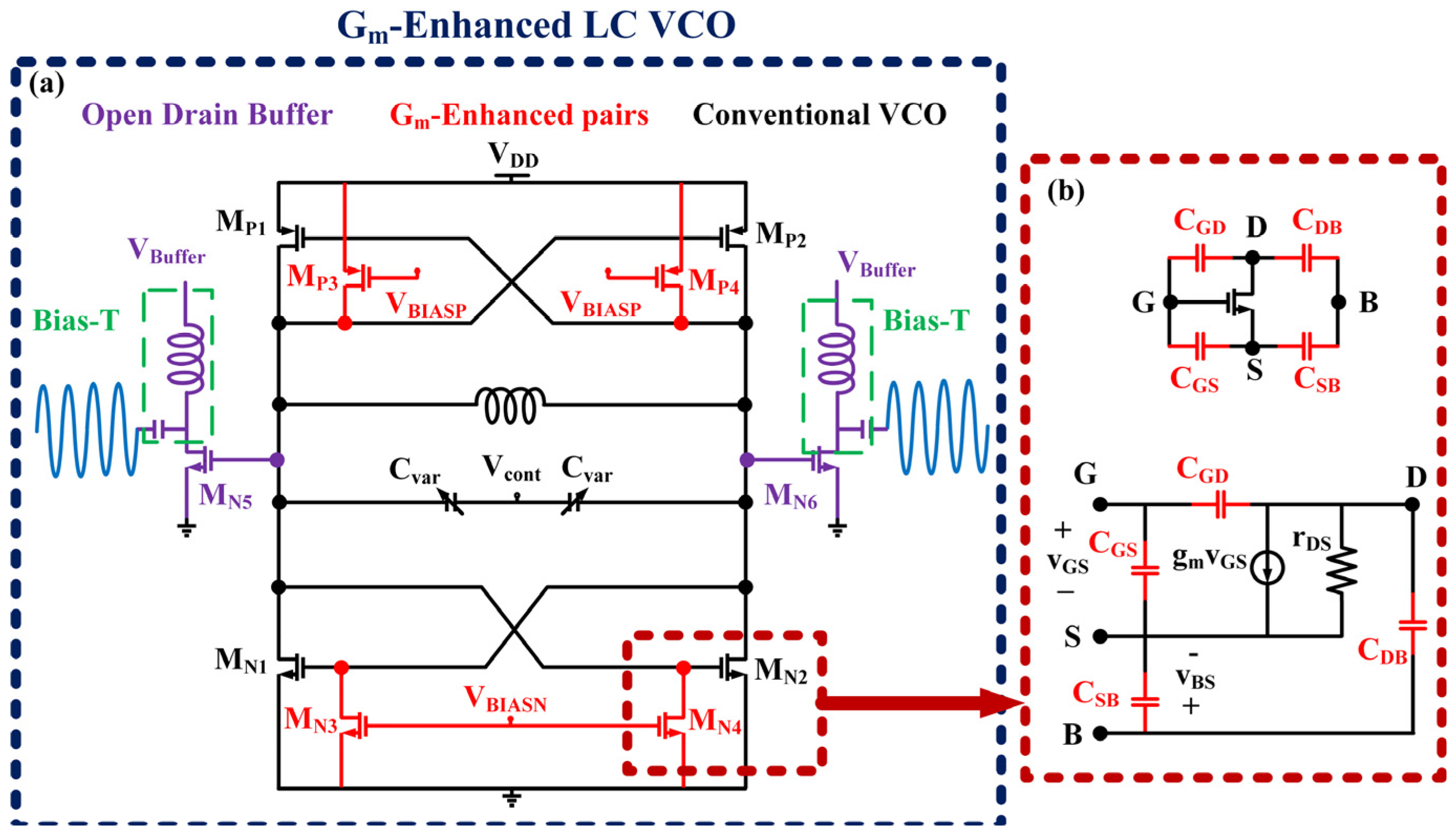
To lower the power consumption of mm-Wave VCOs in widely accessible planar CMOS processes with minimal penalty on PN, area, and TR, the conventional cross-coupled topology should be enhanced/modified. To achieve this goal, innovative topology which takes advantage of undesired intrinsic parasitics of a device is used to generate larger effective G
m at mm-Wave frequencies, thereby presenting a similar negative resistance to the LC tank and sustaining the oscillation at lower power consumption (
Figure 1). The proposed G
m-enhanced architecture utilizes an auxiliary cross-coupled CMOS pair which is connected to the main cross-coupled pair in such way as to increase its effective G
m at high frequencies. Considering the high frequency small signal model (SSM) of a MOS device, the signal coupling to the auxiliary devices through parasitic capacitances such as the C
gd can be substantial at mm-Wave frequencies, presenting a larger negative resistance to the tank, and could potentially allow for lower overall power consumption [
7,
17]. For the first prototype, this paper presents a novel low-power 24-to-29.2 GHz LC VCO which uses G
m-enhanced cross-coupled CMOS pairs to reduce the power consumption and improve the PN performance with minimal impact on the TR (
Figure 1a). The remainder of this paper is structured as follows:
Section 2 briefly introduces the G
m enhancement concept and provides more details about the design of the proposed low-power G
m-enhanced CMOS LC VCO. The VCO measurement results are presented in
Section 3 and compared with the simulation as well as the state-of-the-art LC VCOs in a similar frequency range.
Section 4 provides the concluding remarks.
2. GM-Enhanced LC VCO Design
The proposed G
m-enhanced LC VCO uses a complimentary (i.e., CMOS) cross-coupled topology without a tail current source to maximize the output swing as shown in
Figure 1a. A conventional CMOS LC VCO (CVCO) is also implemented in the same technology and characterized for performance comparison with the proposed G
m-enhanced CMOS LC VCO.
Figure 1a shows the schematic of both VCOs with highlights showing their differences. Both designs use open drain buffers to interface with the measurement equipment. The power consumption, PN, and TR of an LC VCO rely heavily on the g
m of CMOS pairs because the g
m of NMOS and PMOS cross-coupled pairs must satisfy the start-up condition of LC VCO designs, as shown below:
where
RP is the equivalent parallel resistance of the LC tank used in the VCO, and
Gm is the total transconductance of the VCO core. To save power, the
Gm is usually set to a minimum needed to start and sustain the oscillation. Minimizing
Gm is also important in lowering the PN, since the device noise (particularly the flicker) is directly impacted by the device g
m [
6,
8,
10,
18,
19,
20]. In fact, Hajimiri et al. [
20] have shown that a lower PN requires lower g
m from active devices due to the effect of flicker noise on the PN at low offset frequencies. High
Gm is also problematic for the TR as it necessitates using large devices when the supply voltage is limited, increasing the parasitic capacitance of the tank and further limiting the TR [
6,
8,
10]. Therefore, transistor g
m optimization is critical to ensure optimum VCO performance in both voltage-limited and current-limited designs [
18]. In addition to the g
m of NMOS and PMOS cross-coupled pairs, the LC tank plays a key role in the power consumption, PN, and TR performance of an LC VCO, requiring a careful design of tank components, particularly the inductance. On the one hand, increasing the output swing, which directly helps the phase noise, calls for large inductors with the highest quality factor (Q), since the output voltage is proportional to Q
tank × L
tank × ω
osc. On the other hand, the PN is proportional to (L
tank)
2 [
18], suggesting that a low inductance is preferred. The Q variations across the TR should be considered as well, and minimized to limit the PN deterioration across the TR, favouring small inductors at mm-Wave. Moreover, TR is inversely proportional to the L
tank, further incentivizing the use of a small inductor in the tank. Hence, a careful trade-off between the inductance and capacitance of the tank is performed for both VCOs. To further increase the inductor Q and save chip area, the VCOs use differential inductors with a floating center tap [
21]. The geometry of planar inductors is optimized by considering optimization methods in the literature [
22]. The 410 pH inductor designed for the CVCO exhibits a Q of 15.2 near 28 GHz with 69.2 GHz self-resonance frequency (SRF), while the 350 pH inductor designed for the G
m-enhanced LC VCO shows a Q of 16.8 near 28 GHz with SRF > 80 GHz.
Figure 2 shows the Q and inductance of the inductors used in the CVCO and G
m-enhanced VCO tanks.
In addition to the LC tank, the choice of biasing impacts the power consumption. A popular approach in low-power VCOs is to bias the cross-coupled pair in class C to reduce the VCO power consumption [
23]; however, this power reduction comes at the cost of potential start-up failure across process, voltage, and temperature (PVT) corners due to the low gate bias voltage [
23,
24]. In many cases, the requirements for start-up put stringent limitations on the biasing, preventing maximum oscillation amplitude, and hence negatively impacting the PN performance. While dynamic biasing may help to solve this problem, it requires auxiliary voltage detection stages [
23,
24] whose power consumption cannot be ignored in low-power (sub-mW) VCOs. The additional metallic wirings connecting these auxiliary circuits to the main VCO core are also problematic for mm-Wave application as they introduce additional fixed parasitics and limit the TR of the VCO. To avoid these problems, both VCOs presented here avoid class-C biasing.
2.1. Differential Gm-Enhancement Technique
G
m-enhancement (or boosting) techniques are generally categorized into two groups: direct and indirect G
m-enhancement techniques [
6,
7,
8]. Direct G
m-enhanced techniques utilize additional devices that control the current passing through the devices to increase the total
Gm. Examples include adaptive current mirrors [
7], negative gain stage [
25], and g
m-boosting amplifiers [
26,
27]. Direct g
m-boosting techniques generally require additional circuitry with active devices to control the current or amplify the signals. On the other hand, indirect G
m-enhanced techniques benefit from the feedback concept, which could consist of only passive devices if desired [
8]. There are two main approaches for indirect G
m-enhanced techniques: capacitive coupling and magnetic/inductive coupling [
28]. The proposed design employs a hybrid G
m-enhanced structure that aims to share the AC current among multiple devices, at mm-Wave frequencies, to generate larger effective
Gm without increasing the power consumption (
Figure 1a). The enhanced
Gm is then used to generate the required negative resistance needed to sustain the oscillation.
To understand the operation mechanism of the proposed G
m-enhancement technique, a Small Signal Equivalent Circuit (SSEC) of the proposed VCO is developed (
Figure 1b,c). Considering the symmetric nature of the design, half-circuit analysis with differential connection is used (
Figure 1d). The total current, i
ds, is shared between the main devices, i.e., M
N1 and M
N2, and g
m-booster devices, i.e., M
N3 and M
N4. Considering the shared drain (D) and gate (G) connection of these devices,
,
, and
where
is the voltage between G and S of the active device,
is the voltage at G of the active device or D of the g
m-booster device, and
is the voltage at D of the active device. Then, the equivalent circuit can be simplified to
Figure 1e, and analyzed using conventional network theory:
where
is the ratio of the active device current and the total current of the active and the g
m-booster devices,
is the current between G and D of the active device,
is g
m of the active device,
is the current between G and D of the booster device,
is the g
m of the booster device,
is the current between G and S of the active device,
is the impedance of
CGS of the booster device,
is the impedance of
CGS of the active device,
is the impedance of
CGD of the booster device, and X
eq is unitless and ~1/3 since
CGD is considered ~half of the
CGS in strong inversion. To facilitate the design and optimization process, the overdrive voltage (V
ov) that is equal to V
GS-V
TH is set to be roughly the same for both active and g
m-booster devices. The AC currents are defined according to the direction and the device type (active or booster), while the impedances of junction capacitors are defined only based on the device type (active or booster). The parameter
is defined as the ratio of the g
m-booster current,
, to the total branch current passing through both drains,
(
Figure 1e):
where
and
are the total AC drain currents of the booster and active devices that share the same drain current, respectively, and they can be expressed as
From Equations (8)–(11), it is clear that
is a function of the W/L ratio of active and g
m-boosting devices and the frequency, since AC currents are affected by the reactance generated by the devices’ parasitic capacitances. Using Equations (2)–(7), Equations (10) and (11) can be further simplified and written in terms of the angular frequency, ω, and device parasitic capacitances.
is heavily dependent on the
since it generates the
needed for the g
m-booster device, as shown in Equation (6).
,
, and
can be expressed as follows:
where
and
are the gate-source and gate-drain capacitances of the active device and
and
are the gate-source and gate-drain capacitances of the g
m-booster device, respectively. Assuming
~2
in strong inversion, Equations (10) and (11) can be rearranged as:
is directly proportional to the frequency, resulting in
~0 at very low frequencies due to the very small AC current flowing through the
. Choosing proper gate biasing for the g
m-booster device and ignoring the channel-length modulation,
can be rewritten based on critical device parameters:
From Equation (14), it is clear that
→ 0 when ω → 0, leading to
→ 0. Equation (17) also shows that
is maximized at very high frequency when the reactance of the
CGS and
CGD capacitances of the device are made very small and create shorting. At such high frequencies, the maximum value for
(
) can be found as the ratio of the parasitic capacitances of the active and g
m-boosting devices, which is representative of the W/L ratio:
where
. As evident in Equations (8)–(17), the critical user-defined parameter in the design of the proposed g
m-boosting pair is
since it determines the current sharing ratio between the active and g
m-booster devices.
2.2. Proposed Gm-Enhanced LC VCO Design
To sustain oscillation in a cross-coupled CMOS VCO, the loss in the LC tank should be compensated with the negative resistance produced by the cross-coupled pairs (
Figure 1a). As such, the total
Gm of a complimentary cross-coupled LC VCO should satisfy the start-up condition shown in Equation (1). In this work, an innovative topology is proposed to increase the effective
Gm via g
m-booster pairs (
Figure 1a), which is then used to generate the required negative resistance to sustain the oscillation. With the increased
Gm, the proposed cross-coupled pair is capable of sustaining oscillation at a lower power consumption with a similar tank, compared to a CVCO.
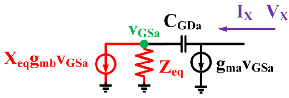
Figure 3 shows the half-circuit equivalent circuit model used to calculate the effective
Gm of the proposed VCO. Using Equation (2) through Equation (7), which show the relationship between v
gs of the active devices and those of the g
m-boosters, the negative impedance can be found. Since G and D terminals of active and g
m-booster devices are shared, impedances of
,
, and
can be grouped into
:
Analyzing the circuit shown in
Figure 3,
and
can be found:
Then, the equivalent output impedance,
, can be found as:
Once the real and imaginary components of
have been separated and
has been expressed in terms of
and
using Equation (17), the effective
Gm of the proposed design can be approximated as:
From Equation (23), it is clear that the proposed structure produces higher
Gm at high frequency when consuming similar power, compared to a conventional cross-coupled pair used in the CVCO.
Figure 4 provides a conceptual view of how the required
Gm for the oscillation start-up is generated in the proposed VCO compared to the CVCO. As demonstrated in Equation (23), the effective
Gm is significantly larger at high frequencies compared to at low frequency. Ideally, the expected
= 0.5 gives the highest effective
Gm when the W/L ratio of the g
m-booster and active devices are equal. Assuming equal length for the devices,
=
,
=
, and 2
CGD~CGS in strong inversion when W
a = W
b. In this case,
~0.25 at high frequency (near the transition frequency, f
T), resulting in ~33% higher effective
Gm. However, the effective
will be smaller for our application where f~30 GHz << f
T (~200 GHz) of the process. Moreover, the width of the g
m-boosting devices is usually chosen to be smaller than those of the width of the active device in low-power design to reduce parasitics and conserve energy. For this design,
~0.2 is chosen, resulting in a maximum
Gm enhancement of ~25%.
To observe the improvement in the effective G
m compared to the CVCO, several sets of simulations are performed in Cadence and the results are plotted in
Figure 5. In these simulations, the impedance of the proposed G
m-enhanced cross-coupled pair (i.e., input impedance) is discovered and compared with those of the standard cross-coupled pair used in the CVCO. Then, the real and imaginary parts of the input impedance are calculated to find the effective
Gm in both cases (
Figure 5a–c). The estimated
Gm calculated from the first-order theoretical analysis given above is also shown in the same plot for the comparison. The effect of frequency on increasing the effective
Gm in the proposed G
m-enhanced cross-coupled pair is clearly seen in the plots. For
~0.2, the proposed G
m-enhanced cross-coupled pair shows a ~19% higher effective
Gm at ~30 GHz compared to the standard cross-coupled pair with similar power consumption (
Figure 5c). The results exhibit
~0.16 at ~30 GHz for the proposed VCO.
3. Characterization Results
The proposed G
m-enhanced VCO is implemented in a 1P9M 65 nm standard CMOS process along with an on-chip open-drain NMOS buffer (connected to GSG pads) used for interfacing with the measurement equipment (
Figure 6). A CVCO with a similar inductor design is also included on the same die for performance comparison (
Figure 6a). To enable accurate performance measurement for these mm-Wave VCOs, both VCOs are characterized using RF probes with external bias-Ts, facilitating the connection to the supply. This way, the loss associated with external components (such as the cables) can be de-embedded from the measurement results. A general view of the test setup is shown in
Figure 6c. Both the G
m-enhanced LC VCO and CVCO dies measure 580 µm × 455 µm. For the proposed design, the VCO core occupies 92 µm × 164 µm (≈0.015 mm
2). The VCO core is slightly larger in the CVCO (due to the larger inductor) and measures 99 µm × 182 µm (≈0.018 mm
2). A Keysight PXA N9030A signal analyzer is used to monitor the output signal and measure the PN performance across the TR. Both VCOs are characterized under similar conditions to allow for accurate comparison. Measurement results show that the proposed G
m-enhanced VCO can sustain oscillation with a power consumption as low as 455 μW (650 μA from 0.7 V supply), while the CVCO burns ≈ 608 μW (760 μA from 0.8 V supply) to sustain the oscillation, clearly showing the power advantage of the proposed VCO. Moreover, the superior PN performance of the G
m-enhanced VCO can be observed when comparing both designs at similar output power ~−11 dBm (
Figure 7a). The proposed G
m-enhanced VCO exhibits measured PN performance ~−106.5 dBc/Hz and −132.0 dBc/Hz at 1 MHz and 10 MHz, respectively, @24.5 GHz when the V
DD is set to 0.8 V (P
DC~880 μW). On the other hand, CVCO achieves a measured PN~−97.1 dBc/Hz and −122.6 dBc/Hz at 1 MHz and 10 MHz, respectively, at a similar frequency (~25 GHz) when the V
DD is set to 1 V (P
DC~1.5 mW). The PN floor for both designs reaches ~−140 dBc/Hz (
Figure 7). The proposed VCO’s PN performance is relatively stable across the tuning range, with negligible deterioration (<2 dBc/Hz) at the upper end of the tuning range. In this case, the PN measures ~−104.7 dBc/Hz and −131.4 dBc/Hz at 1 MHz and 10 MHz, respectively (
Figure 7b).
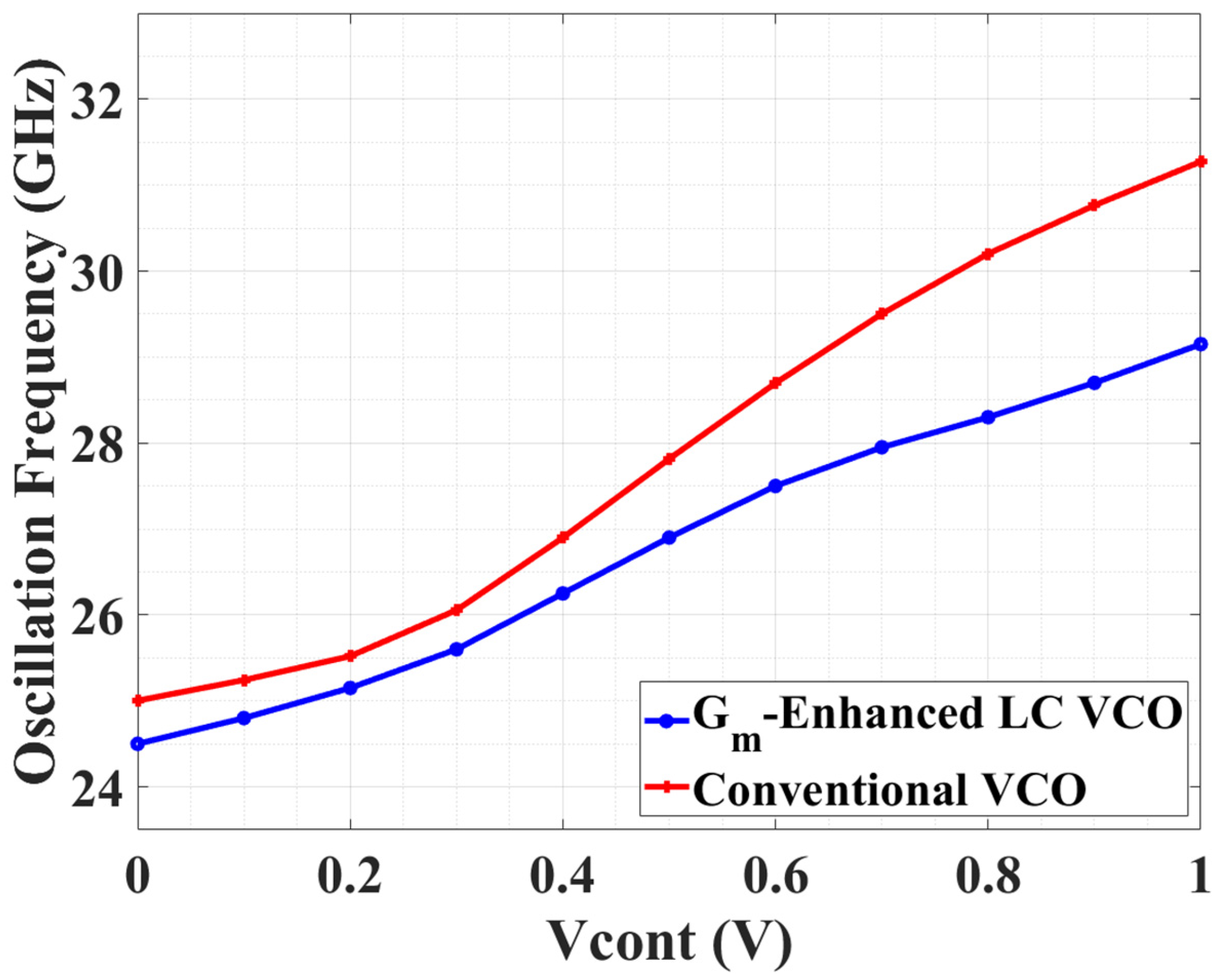
At V
DD = 0.8 V (P
DC~880 µW), the oscillation frequency changes from ~24.5 GHz to ~29.1 GHz for the G
m-enhanced VCO, demonstrating a TR of 4.6 GHz (~17.8%) (
Figure 8). On the other hand, the CVCO oscillation frequency changes from ~25 GHz to ~31.2 GHz at V
DD = 1 V (P
DC~1.5 mW), demonstrating a TR of 6.2 GHz (~24.5%) (
Figure 8). Some PN variations across TR are expected due to the change in the Q of the tank across the frequency range. However, the PN performance is relatively stable (±5 dB) across the TR at 1 MHz and 10 MHz offset. Considering the ~1 GHz shift between the simulated and measured oscillation frequency, the measured PN is also in good agreement with the simulation (
Figure 9).
The deterioration in the TR of the proposed VCO is due to the extra capacitance resulting from parasitics of additional cross-coupled pairs and additional metal wiring in the layout. However, the slight closed-in PN improvement (esp. foffset < 1 MHz) in the proposed VCO compared to the CVCO requires a more detailed analysis.
Different PN models for LC VCOs are presented in the literature [
19,
20,
29]. The proposed design shows significantly improved PN performance for low offset frequency, with the Flicker noise dominant area with 1/f
3 slope [
19]. As such, Hajimiri’s PN model [
20] is preferred. Hajimiri’s model aims to accurately predict the PN of an LC VCO in the 1/f
3 and 1/f
2 regions. For accurate predictions, this model needs impulse sensitivity function (ISF), which is a periodic and dimensionless function. ISF is a periodic function, so Fourier coefficients can be used to represent the ISF function:
where
is the first coefficient of the ISF, and is equal to 2Γ
DC, the coefficients (Γ
n) are real values, and
θn is the phase of the nth harmonic.
θn is small and can be ignored at random input noise [
20], and the coefficients can be estimated analytically or calculated from the simulation. To calculate the coefficients from the simulation, HB and HBnoise simulations of the Cadence Spectre engine provide the perturbation projection vector (PPV) that represents the sensitivity of the per cycle jitter variance to current perturbations at the nodes of the oscillator [
29], and can be used to estimate the ISF changes [
20,
29].
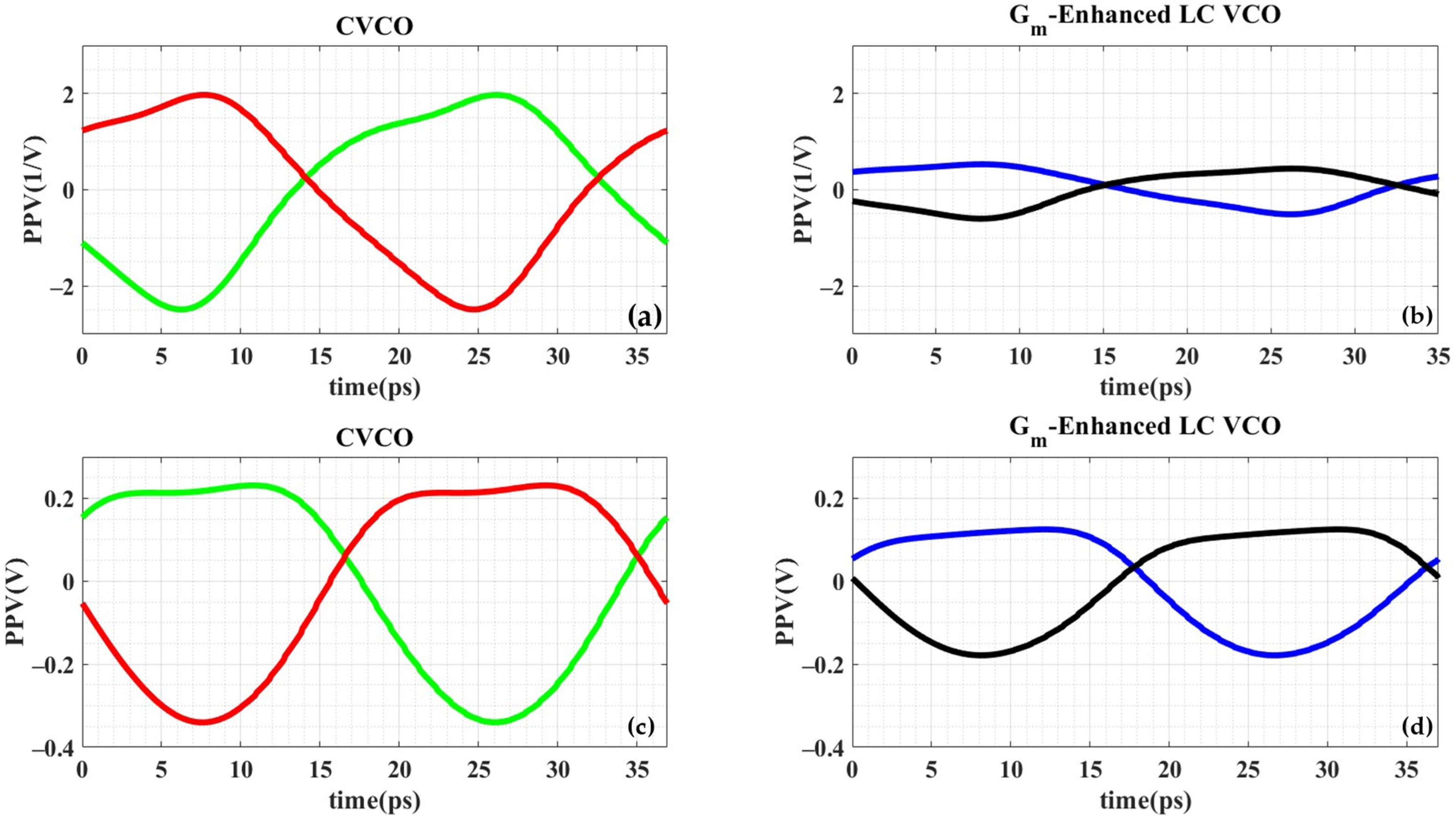
In this work, PPV results can be obtained from the HB and HBnoise simulations (
Figure 10). HB PPV results are presented in V and HB noise PPV results are shown in 1/V. Then, the PN model for the 1/f
3 region can be defined as:
where
is the total noise current,
. The term
is the power spectral density of the noise of active devices and
is the power spectral density (PSD) of the thermal noise current due to
Rp;
is the maximum charge displacement across the equivalent output capacitance where the impulse was injected, and
is
corner frequency. At low offset frequencies, the flicker noise of the MOS device will be the dominant component among these two; hence,
can be expressed as
, where
is the flicker noise fitting parameter,
is the gate oxide capacitance per unit area, and
and
are the transistor width and length, respectively. Assuming that the thermal and flicker noises are uncorrelated, their impact on the PN can be studied separately:
where
is the Boltzman constant,
is the temperature in Kelvin,
is the RMS current consumption of the VCO,
is the fitting parameter for the noise of MOSFET,
is the quality factor of the inductor, and
is the oscillation frequency, respectively. For a design scenario with a given device size, Q, R, and a fixed current consumption budget, the flicker noise contribution to the PN, shown in Equation (26), can be minimized when the PPV is minimized and
is maximized. In this work, the simulation results reveal that the proposed G
m-enhanced VCO exhibited significantly smaller PPV compared to the CVCO; the use of HB simulations revealed Γ
0~0.0071 V and 0.0536 V for the differential output of the proposed VCO compared to Γ
0~−0.0533 V and 0.1539 V for the differential outputs of the CVCO. Similarly, Γ
0~0.3707 1/V and −0.2356 1/V was obtained for the differential outputs of the proposed VCO from the HB noise simulation, while Γ
0~1.2306 1/V and −1.1028 1/V for the differential outputs of the CVCO (
Figure 10). The minimum ratio within Γ
0 for the two VCOs is ~2.9×, which amounts to ~9 dB improvement in the close-in PN for the proposed G
m-enhanced VCO. Moreover, the proposed VCO inevitably has larger
compared to the CVCO due to larger parasitic capacitors from the additional cross-coupled pairs and the resulting on-chip metal wiring. This larger
further improves the close-in PN performance of the proposed VCO. The measured PN results presented in
Figure 7 reveal an up to ~11 dB improvement in the PN at 100 kHz offset for the proposed VCO compared to the CVCO. As the frequency increases, the effect of the flicker noise diminishes, and the thermal noise of active devices and the LC tank parameters (Q and R) become the dominant factors affecting the PN [
10,
18]. Considering equation (27), it can be seen that the thermal component of the PN is mostly affected by the circuit parameters. Given a similar Q for the tank and the output power, the difference in PN for the two VCOs is primarily determined by the difference in the effective
Gm, which is relatively small (~20%). As such, the difference between the PN of two VCOs gradually narrows until it becomes negligible at high offset frequencies near the PN floor.
Figure of merit (FoM) and figure of merit with TR (FoM
T) are important metrics in benchmarking the performance of VCOs. The G
m-enhanced LC VCO measurement results reveal competitive FoM and FoM
T performance. The G
m-enhanced LC VCO shows a FoM of 195.2 dBc/Hz and 200.3 dBc/Hz at 1 MHz and 10 MHz offset, respectively, with a FoM
T reaching 200.4 dBc/Hz and 205.2 dBc/Hz at respective offset frequencies, a significant improvement over those of the CVCO. Compared to the state-of-the-art LC CMOS VCOs [
4,
12,
14,
15,
30] operating at a similar frequency range and fabricated in a similar process node, the G
m-enhanced LC VCO provides comparable performance while burning less power (
Table 1).


