
A Low-Intensity Pulsed Ultrasound Interface ASIC for Wearable Medical Therapeutic Device Applications


Abstract
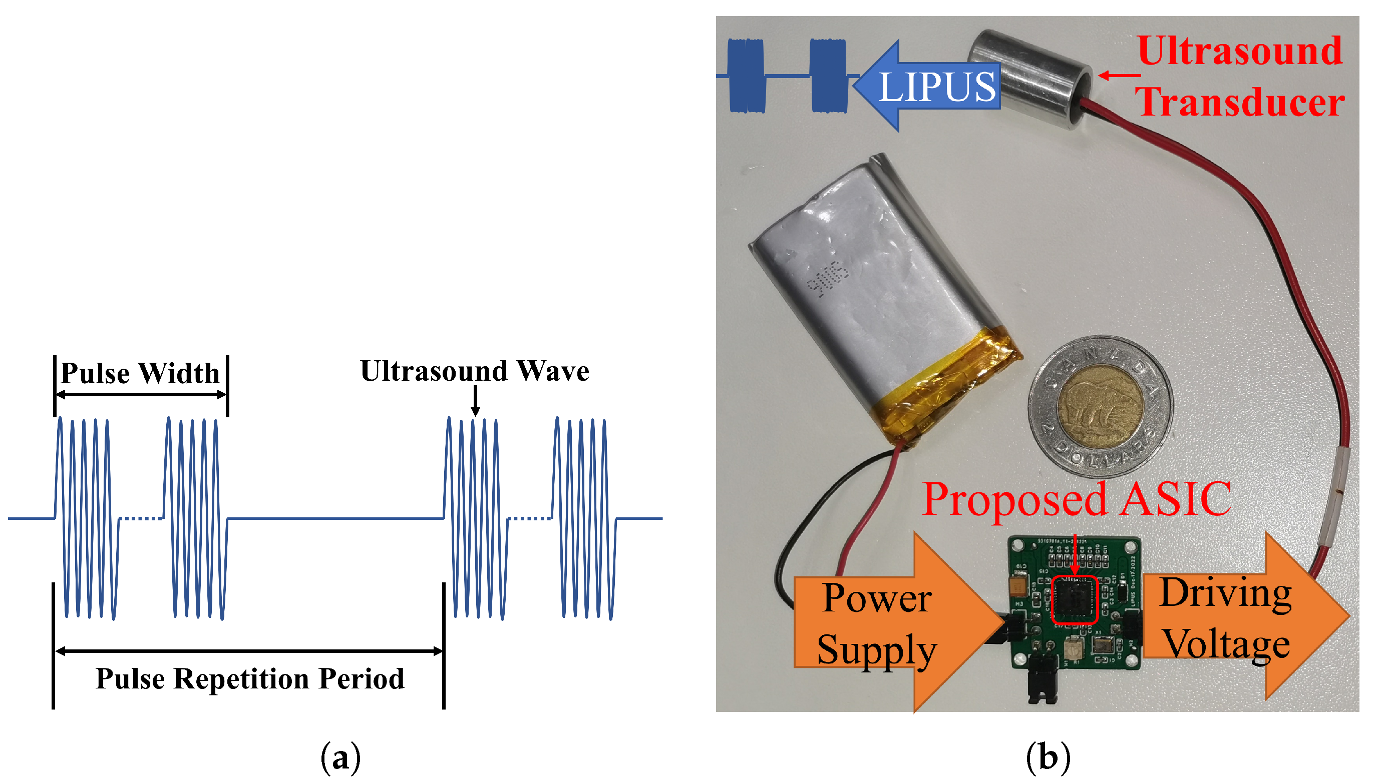
:1. Introduction
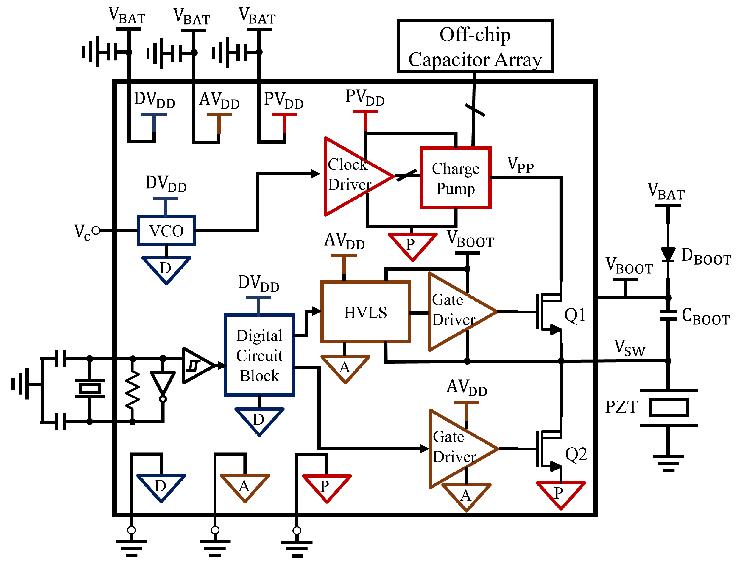
2. System Architecture and Implementation
2.1. Charge Pump
2.2. High Voltage Level Shifter
2.3. Half-Bridge Driver
2.4. Voltage Controlled Oscillator
3. Results and Discussion
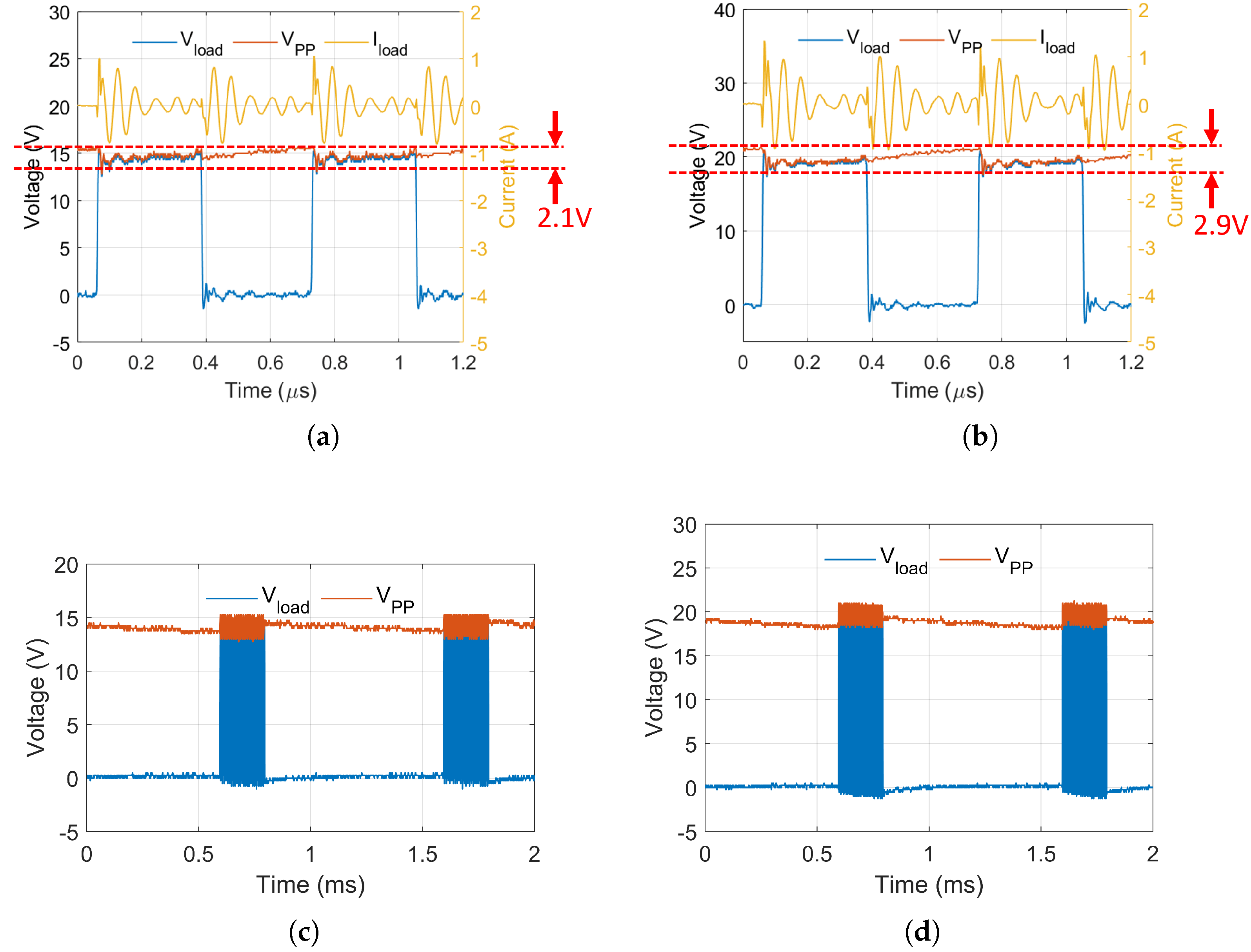
3.1. Simulation Results
3.2. Test Results
3.3. Discussion
4. Conclusions
Author Contributions
Funding
Data Availability Statement
Conflicts of Interest
Abbreviations
| LIPUS | Low-intensity pulsed ultrasound |
| SATA | Spatial average temporal average |
| FDA | Food and Drug Administration |
| NICE | National Institute for Health and Care Excellence |
| ASIC | Application-specific integrated circuit |
| MRI | Magnetic resonance imaging |
| HVLS | High voltage level shifter |
| HB | Half-bridge |
| VCO | Voltage-controlled oscillator |
| CTS | Charge transfer switch |
| CSVCRO | Current-starved voltage-controlled ring oscillator |
References
- Ensminger, D.; Bond, L.J. Ultrasonics: Fundamentals, Technologies, and Applications; CRC Press: Boca Raton, FL, USA, 2011. [Google Scholar]
- Wood, R.W.; Loomis, A.L. XXXVIII. The physical and biological effects of high-frequency sound-waves of great intensity. Lond. Edinb. Dublin Philos. Mag. J. Sci. 1927, 4, 417–436. [Google Scholar] [CrossRef]
- Rubin, C.; Bolander, M.; Ryaby, J.P.; Hadjiargyrou, M. The use of low-intensity ultrasound to accelerate the healing of fractures. JBJS 2001, 83, 259. [Google Scholar] [CrossRef]
- Wood, A.K.; Sehgal, C.M. A review of low-intensity ultrasound for cancer therapy. Ultrasound Med. Biol. 2015, 41, 905–928. [Google Scholar] [CrossRef] [PubMed]
- Beccaria, K.; Canney, M.; Bouchoux, G.; Puget, S.; Grill, J.; Carpentier, A. Blood-brain barrier disruption with low-intensity pulsed ultrasound for the treatment of pediatric brain tumors: A review and perspectives. Neurosurg. Focus 2020, 48, E10. [Google Scholar] [CrossRef] [PubMed]
- Fomenko, A.; Neudorfer, C.; Dallapiazza, R.F.; Kalia, S.K.; Lozano, A.M. Low-intensity ultrasound neuromodulation: An overview of mechanisms and emerging human applications. Brain Stimul. 2018, 11, 1209–1217. [Google Scholar] [CrossRef] [PubMed]
- Acheta, J.; Stephens, S.B.; Belin, S.; Poitelon, Y. Therapeutic Low-Intensity Ultrasound for Peripheral Nerve Regeneration—A Schwann Cell Perspective. Front. Cell. Neurosci. 2022, 15, 544. [Google Scholar] [CrossRef]
- Zhou, X.Y.; Zhang, X.X.; Yu, G.Y.; Zhang, Z.C.; Wang, F.; Yang, Y.L.; Li, M.; Wei, X.Z. Effects of low-intensity pulsed ultrasound on knee osteoarthritis: A meta-analysis of randomized clinical trials. BioMed Res. Int. 2018, 2018, 7469197. [Google Scholar] [CrossRef]
- Uddin, S.M.; Komatsu, D.E. Therapeutic potential low-intensity pulsed ultrasound for osteoarthritis: Pre-clinical and clinical perspectives. Ultrasound Med. Biol. 2020, 46, 909–920. [Google Scholar] [CrossRef] [PubMed]
- El-Bialy, T.; Farouk, K.; Carlyle, T.D.; Wiltshire, W.; Drummond, R.; Dumore, T.; Knowlton, K.; Tompson, B. Effect of low intensity pulsed ultrasound (LIPUS) on tooth movement and root resorption: A prospective multi-center randomized controlled trial. J. Clin. Med. 2020, 9, 804. [Google Scholar] [CrossRef]
- Zhao, X.; Zhao, G.; Shi, Z.; Zhou, C.; Chen, Y.; Hu, B.; Yan, S. Low-intensity pulsed ultrasound (LIPUS) prevents periprosthetic inflammatory loosening through FBXL2-TRAF6 ubiquitination pathway. Sci. Rep. 2017, 7, 45779. [Google Scholar] [CrossRef]
- Poolman, R.W.; Agoritsas, T.; Siemieniuk, R.A.; Harris, I.A.; Schipper, I.B.; Mollon, B.; Smith, M.; Albin, A.; Nador, S.; Sasges, W.; et al. Low intensity pulsed ultrasound (LIPUS) for bone healing: A clinical practice guideline. BMJ 2017, 356, j576. [Google Scholar] [CrossRef]
- Warden, S.J.; Bennell, K.L.; McMeeken, J.M.; Wark, J.D. Can conventional therapeutic ultrasound units be used to accelerate fracture repair? Phys. Ther. Rev. 1999, 4, 117–126. [Google Scholar] [CrossRef]
- Farkash, U.; Bain, O.; Gam, A.; Nyska, M.; Sagiv, P. Low-intensity pulsed ultrasound for treating delayed union scaphoid fractures: Case series. J. Orthop. Surg. Res. 2015, 10, 72. [Google Scholar] [CrossRef]
- Dijkman, B.G.; Sprague, S.; Bhandari, M. Low-intensity pulsed ultrasound: Nonunions. Indian J. Orthop. 2009, 43, 141. [Google Scholar]
- Ang, W.T.; Yu, C.; Chen, J.; El-Bialy, T.; Doschak, M.; Uludag, H.; Tsui, Y. System-on-chip ultrasonic transducer for dental tissue formation and stem cell growth and differentiation. In Proceedings of the 2008 IEEE International Symposium on Circuits and Systems, Seattle, WA, USA, 18–21 May 2008; pp. 1818–1821. [Google Scholar]
- Ang, W.T.; Scurtescu, C.; Hoy, W.; El-Bialy, T.; Tsui, Y.Y.; Chen, J. Design and implementation of therapeutic ultrasound generating circuit for dental tissue formation and tooth-root healing. IEEE Trans. Biomed. Circuits Syst. 2009, 4, 49–61. [Google Scholar] [CrossRef]
- Sensor Technology Ltd. Piezoelectric Material Specifications. 2021. Available online: https://sensortechcanada.com/wp-content/uploads/2021/08/Piezo-spec-sheet_Final.pdf (accessed on 1 August 2021).
- APC International, Ltd. Ultrasonic Power Transducers. 2021. Available online: https://www.americanpiezo.com/standard-products/ultrasonic-power-transducers.html (accessed on 25 January 2023).
- Physik Instrumente. Piezoelectric Disks. 2022. Available online: https://www.pi-usa.us/fileadmin/user_upload/physik_instrumente/files/datasheets/PRYY-Datasheet.pdf (accessed on 23 November 2022).
- Hynynen, K. MRI-guided focused ultrasound treatments. Ultrasonics 2010, 50, 221–229. [Google Scholar] [CrossRef] [PubMed]
- Schlesinger, I.; Sinai, A.; Zaaroor, M. MRI-guided focused ultrasound in Parkinson’s disease: A review. Park. Dis. 2017, 2017, 8124624. [Google Scholar] [CrossRef] [PubMed]
- Zafar, A.; Quadri, S.A.; Farooqui, M.; Ortega-Gutiérrez, S.; Hariri, O.R.; Zulfiqar, M.; Ikram, A.; Khan, M.A.; Suriya, S.S.; Nunez-Gonzalez, J.R.; et al. MRI-Guided High-Intensity Focused Ultrasound as an Emerging Therapy for Stroke: A Review. J. Neuroimaging 2019, 29, 5–13. [Google Scholar] [CrossRef] [PubMed]
- Jiang, X.; Yu, X.; Moez, K.; Elliott, D.G.; Chen, J. High-efficiency charge pumps for low-power on-chip applications. IEEE Trans. Circuits Syst. I: Regul. Pap. 2017, 65, 1143–1153. [Google Scholar] [CrossRef]
- Jiang, X.; Ng, W.T.; Chen, J. A miniaturized low-intensity ultrasound device for wearable medical therapeutic applications. IEEE Trans. Biomed. Circuits Syst. 2019, 13, 1372–1382. [Google Scholar] [CrossRef] [PubMed]
- Halesh, M.; Rasane, K.; Rohini, H. Design and implementation of voltage control oscillator (vco) using 180nm technology. In Proceedings of the International Conference on Advances in Computing, Communication and Control, Kochi, India, 22–24 July 2011; Springer: Berlin/Heidelberg, Germany, 2011; pp. 472–478. [Google Scholar]
- Kaur, H.; El-Bialy, T. Shortening of overall orthodontic treatment duration with low-intensity pulsed ultrasound (LIPUS). J. Clin. Med. 2020, 9, 1303. [Google Scholar] [CrossRef] [PubMed]
- Gopalan, A.; Panneerselvam, E.; Doss, G.T.; Ponvel, K.; Vb, K.R. Evaluation of Efficacy of Low Intensity Pulsed Ultrasound in Facilitating Mandibular Fracture Healing—A Blinded Randomized Controlled Clinical Trial. J. Oral Maxillofac. Surg. 2020, 78, 997-e1. [Google Scholar] [CrossRef] [PubMed]
- Shobara, K.; Ogawa, T.; Shibamoto, A.; Miyashita, M.; Ito, A.; Sitalaksmi, R.M. Osteogenic effect of low-intensity pulsed ultrasound and whole-body vibration on peri-implant bone. An experimental in vivo study. Clin. Oral Implant. Res. 2021, 32, 641–650. [Google Scholar] [CrossRef]
- Xie, S.; Jiang, X.; Wang, R.; Xie, S.; Hua, Y.; Zhou, S.; Yang, Y.; Zhang, J. Low-intensity pulsed ultrasound promotes the proliferation of human bone mesenchymal stem cells by activating PI3K/AKt signaling pathways. J. Cell. Biochem. 2019, 120, 15823–15833. [Google Scholar] [CrossRef]
- Li, Z.; Hua, Y.; Zhang, J.; Fu, Z. Low-intensity pulsed ultrasound promotes the proliferation of bone marrow mesenchymal stem cells by inducing cyclin D1 up-regulation. Chin. J. Tissue Eng. Res. 2022, 26, 2006. [Google Scholar]
- Hofmann, K.; Shen, L.; González-Rodríguez, E.; Maune, H.; Shah, I.A.; Dahlhaus, D.; Jakoby, R. Fully integrated high voltage charge pump for energy-efficient reconfigurable multi-band RF-transceivers. In Proceedings of the Intelec 2012, Scottsdale, AZ, USA, 30 September–4 October 2012; pp. 1–4. [Google Scholar]
- Lin, S.P.; Ker, M.D. Design of stage-selective negative voltage generator to improve on-chip power conversion efficiency for neuron stimulation. IEEE Trans. Circuits Syst. I: Regul. Pap. 2020, 67, 4122–4131. [Google Scholar] [CrossRef]
- Zeng, X.; Zhang, X.; Yao, L.; Xue, N. A 15.4 V Fully-Integrated Energy-Efficient Pulse Generator in Standard 0.18 μm CMOS. IEEE Trans. Circuits Syst. II Express Briefs 2020, 68, 1812–1816. [Google Scholar]
- Abaravicius, B.; Moldovan, A.; Cochran, S.; Mitra, S. Development of a Point-of-Care Ultrasound Driver for Applications with Low Power and Reduced Area Requirements. In Proceedings of the 2021 IEEE International Ultrasonics Symposium (IUS), Virtual, 11–16 September 2021; pp. 1–4. [Google Scholar]
- Ballo, A.; Grasso, A.D.; Palumbo, G. A review of charge pump topologies for the power management of IoT nodes. Electronics 2019, 8, 480. [Google Scholar] [CrossRef]


| Transistors in Charge Pump | Type | W/L (μm/μm) |
|---|---|---|
| MA1, MB1 | 20 V HVNMOS | 2200/0.5 |
| MA2-5, MB2-5 | 20 V HVPMOS | 2700/1 |
| MNA2-4, MNB2-4 | 20 V HVNMOS | 300/0.5 |
| MPA2-4, MPB2-4 | 20 V HVPMOS | 1800/1 |
| Transistors in HVLS | Type | W/L (μm/μm) |
| M1, M2 | 50 V HVNMOS | 10/0.5 |
| M3, M4 | 50 V HVPMOS | 10/1 |
| M5, M6 | 5V PMOS | 0.5/0.5 |
| Transistors in CSVCRO | Type | W/L (μm/μm) |
| M1 | 5V PMOS | 1.2/1 |
| M2 | 5V NMOS | 0.6/1 |
| M3, M7, M11 | 5V PMOS | 6/0.5 |
| M4, M8, M12 | 5V PMOS | 9/0.5 |
| M5, M9, M13 | 5V NMOS | 4.5/0.5 |
| M6, M10, M14 | 5V NMOS | 3/0.5 |
| Transistors in Half Bridge | Type | W/L (μm/μm) |
| Q1, Q2 | 50 V HVNMOS | 10,000/0.5 |
| Power | Component | Direction | Power | Efficiency |
|---|---|---|---|---|
| 3.7 V | HB transducer driver | input | 89.2 | 96.97% |
| output | 86.5 | |||
| DC-DC booster converter | input | 242 | 36.86% | |
| output | 89.2 | |||
| Whole chip | input | 244 | 35.45% | |
| output | 86.5 | |||
| 5 V | HB transducer driver | input | 170.7 | 96.95% |
| output | 165.5 | |||
| DC-DC booster converter | input | 454.8 | 37.53% | |
| output | 170.7 | |||
| Whole chip | input | 457.7 | 36.16% | |
| output | 165.5 |
| Power supply (V) | 3.7 | 5 |
| Input power of the chip (mW) | 347.8 | 620 |
| Output power to the load (mW) | 107.2 | 184.2 |
| Power conversion efficiency of the chip | 30.8% | 29.7% |
| Output ultrasound power (mW) | 28 | 49 |
| Output ultrasound Power intensity (mW/cm2) | 29.5 | 51.6 |
| Work | This Work | [25] | [32] | [33] | [34] |
|---|---|---|---|---|---|
| Technology | 0.35 μm HVCMOS | 0.18 μm HVCMOS | 0.35 μm HVCMOS | 0.25 μm BCD | 0.18 μm CMOS |
| (V) | 5 (3.7) | 3.7 | 3.7 | 3 | 3.3 |
| # of stage | 4 | 4 | 36 | 4 | 4 |
| (V) | 21.5 (15.5) | 14 | 120 | 9.3 | 15.4 |
| Frequency | 10–60 MHz | 20 MHz | 10 MHz | N/A | 30 MHz |
| Capacitor | 4.7 nF off-chip | 132 pF on-chip | N/A | 100 pF on-chip | 180 pF on-chip |
| Efficiency | 29.7% (30.8%) | 17% | 12.6% | 41% @ 49.5 mW | 32.3% @ 8.2 mW |
| Output Power (mW) | 184.2 (107.2) | 72 | 13.7 | 49.5 | 8.2 |
| Die area (mm2) | 2.0 × 2.0 | N/A | 3.9 × 5.6 | 2.01 × 1.12 | 0.7 × 0.8 |
Disclaimer/Publisher’s Note: The statements, opinions and data contained in all publications are solely those of the individual author(s) and contributor(s) and not of MDPI and/or the editor(s). MDPI and/or the editor(s) disclaim responsibility for any injury to people or property resulting from any ideas, methods, instructions or products referred to in the content. |
© 2024 by the authors. Licensee MDPI, Basel, Switzerland. This article is an open access article distributed under the terms and conditions of the Creative Commons Attribution (CC BY) license (https://creativecommons.org/licenses/by/4.0/).
Share and Cite
Ye, X.; Jiang, X.; Wang, S.; Chen, J. A Low-Intensity Pulsed Ultrasound Interface ASIC for Wearable Medical Therapeutic Device Applications. Electronics 2024, 13, 1154. https://doi.org/10.3390/electronics13061154
Ye X, Jiang X, Wang S, Chen J. A Low-Intensity Pulsed Ultrasound Interface ASIC for Wearable Medical Therapeutic Device Applications. Electronics. 2024; 13(6):1154. https://doi.org/10.3390/electronics13061154
Chicago/Turabian StyleYe, Xuanjie, Xiaoxue Jiang, Shuren Wang, and Jie Chen. 2024. "A Low-Intensity Pulsed Ultrasound Interface ASIC for Wearable Medical Therapeutic Device Applications" Electronics 13, no. 6: 1154. https://doi.org/10.3390/electronics13061154