1. Introduction
DC–DC converters are extensively used in many applications of power conversion. DC voltage is increasingly used in lighting, renewable energy sources, energy storage integration, data centers, motor drives, and many other applications [
1]. With further improvements to wide-bandgap (WBG) devices, such as gallium nitride (GaN) and silicon carbide (SiC) transistors, it is possible to increase the switching frequency without a significant loss increase, thus improving the power density of DC–DC converters [
2]. Comparing GaN to silicon (Si) devices, they have higher carrier mobility, lower on-state resistance, and lower parasitic capacitance. This gives them advantages such as being able to be turned on and off more quickly and lower on-state losses, resulting in better efficiency at higher switching frequencies. The application of GaN transistors and an increase in the switching frequency allow for the development of improved converter topologies and control solutions [
3]. A higher switching frequency potentially allows a control system with a faster response to be designed because the cut-off frequency should be at least two times lower than the switching frequency [
4]. There are many possible solutions to consider for the implementation of analog or digital controllers. Digital control offers better flexibility compared to analog control, and in many applications this allows for the implementation of additional features or additional control loops without additional expenses. With recent advancements in DC grids and microgrids, the fast and stable control of voltage has become even more important [
5,
6], and, therefore, voltage control will be the focus of this paper.
Digital control allows for the implementation of many different modes, modulation strategies, and digital control algorithms [
7]. To further improve the performance of a control system, more advanced algorithms can be used, such as adaptive control, which is summarized in [
8]; autotuning methods to improve control in a specific operational situation, as shown in [
9]; or the self-identification methods implemented in [
10] to measure a model of a converter and then optimize the converter. Although these advanced controller algorithms show the high-performance potential of digital control, they require high-performance microcontrollers or field-programmable gate arrays (FPGAs), and they are not easy to implement without the introduction of complex math and specific hardware solutions.
Analog controllers for DC–DC converter control have long been used, and many engineers and researchers have the skills to design them properly [
11]. In practice and in the scientific literature, such as [
12,
13,
14], time-domain design methods are sometimes used for controllers, but this usually does not lead to optimal control performance. Frequency-domain design techniques are most often used and are well described, such as in [
15]. In that case, the controller is designed by determining the Bode plot of the converter and the requirements regarding the cut-off frequency (
fc) and phase margin (φ
PM). The cut-off frequency characterizes the speed of the controller, and the phase margin characterizes the stability and overshoot of the controller. To design a stable digital controller, two approaches are usually used: the application of analog controller design methods taking into account delays and their digital nature, and direct digital design in a discrete-time z-domain [
16]. The first approach is easier to understand since it relies on a traditional design technique, but it can also introduce errors since zero-order hold (ZOH) and computational delay should be considered in a digital closed-loop design [
17,
18].Although it was demonstrated in [
19] that direct digital design in the z-plane provides good performance, this approach requires the discretization of the converter transfer function, which is computationally intensive and requires deep knowledge of control theory and more advanced simulation software and models. Therefore, the first approach is beneficial and gives good results if the digital nature of the controller is considered.
The goal of this paper is to provide a practical and intuitive guide for digital controller design via improved methodology, considering delays introduced by the digital nature of a controller in more detail. For a fast controller, the cut-off frequency should be as high as possible. If the cut-off frequency is close to the sampling frequency, the phase distortion becomes noticeable and plays an important role in stable controller design, which is not the case for an analog controller. Although in [
20,
21] models of an analog-to-digital converter (ADC) and a pulse-width modulator (PWM) are presented, this distortion is not analyzed from a practical point of view. Such analysis will be provided in this paper. A practical method for designing a digital controller based on Bode plot measurements will be shown further in this paper. The delays introduced by digital control will be analyzed and compared with a simulation and experimental results.
2. GaN-Based DC–DC Converter and Its Bode Plot
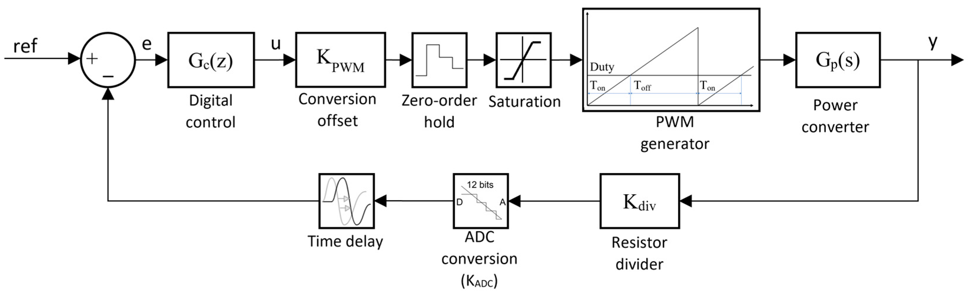
Insulated-gate bipolar transistors (bipolar transistors combined with a metal–oxide–semiconductor structure for control) (IGBTs), silicon (Si) metal–oxide–semiconductor field-effect transistors (MOSFETs), or wide-bandgap (GaN and SiC) devices can be used as semiconductor devices for DC–DC converters. For low-voltage applications, Si MOSFETs or GaN transistors are the most common devices, while for high voltages, IGBTs are often used. The application of GaN transistors makes it possible to increase the switching frequency with the potential to reduce the response time of a converter, but a proper controller should be developed. The goal of this study was to design a fast digital controller for a GaN-based converter working with a high switching frequency. The digital control was compared to an analog controller, which was to be implemented on a Si transistor-based converter prototype.
A simplified circuit of a DC–DC converter with digital control of the output voltage can be seen in
Figure 1. A particular converter is proposed to control power flow between a DC microgrid and energy storage. To achieve the bidirectional capability of the converter, current control needs to be used. While current control is necessary to achieve the bidirectional control of such a converter, the scope of this study was to design voltage control because, in many cases, it is critical that voltage control is fast and that the voltage level remains in the desired range. Further analysis provided here is universal and can also be applied to other control loops.
Texas Instruments (TI) LMG5200MOFT GaN transistors with an integrated gate driver were used for the experimental DC–DC converter design. They offered a relatively small footprint, and the two transistors inside the integrated circuit (IC) were connected in a half-bridge configuration. This solution also simplified the PCB design because the parasitic inductance in the switching loop could be reduced more easily. To drive the transistor gates, a voltage of 5 V (V
CC), which was recommended in the datasheet, was used. For high-side switching, the IC had an integrated diode for bootstrapping purposes and had dedicated outputs for a bootstrapping capacitor. Because of the integrated driver, the control of the gates was made transistor–transistor logic (TTL) compatible with a voltage level up to 12 V, but the threshold for gate activation was 2 V and was, therefore, compatible with STM32G4 3.3 V logic. A switching frequency of 500 kHz was selected for the converter because higher frequencies led to overheating of the transistors. For the control of the converter, an STM32G4 microcontroller was used. This microcontroller offered features such as a filter math accelerator (FMAC), a high-resolution timer (HRTIM), an ADC, and a processor working at frequencies up to 170 MHz [
22], and was available for a relatively low cost. In this article, an analysis of how to implement a fast digital control algorithm with this inexpensive microcontroller is provided, and the provided methodology can also be applied to any digital controller. The introduced delays should be adjusted in that case.
A universal GaN transistor-based board was developed with three previously mentioned TI GaN transistor-based ICs to have the ability to use this board for motor drive applications. In this case, only one of the three half bridges was utilized. The experimental prototype can be seen in
Figure 2. Inductor and output capacitors were placed on another board where analog control was implemented, which will be shown later. An output filter with a 6 µH inductor and an 18.8 µF capacitor, which had an equivalent series resistance (ESR) of 30 mΩ, was used in the experiments with digital control. The desired output voltage was equal to 12 V, and loads ranging from 2 Ω to 5 Ω were selected for the experiments. The maximum power of the converter was equal to 100 W.
The theoretical transfer function of a DC–DC converter in buck mode is available in the literature [
23,
24] and other sources. By putting the values of a converter’s passive elements in a buck converter’s open-loop control-to-output voltage transfer function, it is possible to obtain the transfer function. The poles and zeros of the transfer function can be calculated as follows [
22]:
where
ω0 and
ωESR are the output LC filter complex double pole and the output capacitor ESR zero. The damping factor (
Q) and transfer function (
can be expressed as follows:
After obtaining the theoretical transfer function using Equation (4), it is possible to draw a Bode plot and analyze the converter’s stability with different controllers. A theoretical model can introduce significant error, leading to converter instability; therefore, experimental measurement of a Bode plot is preferable in many cases to increase the accuracy of the transfer function, which leads to more accurate controller design. To measure the practical open-loop response of a converter, a frequency response analyzer is the best option. A wide range of devices are available on the market. A response analyzer has an injection transformer that is used to inject a small signal in a wide range of frequencies at the circuit’s points of interest. From these measurements, a Bode plot is created with frequency response analyzer manufacturer-provided software. To obtain these measurements, there is a need for some control. Although it can be very slow or with poor performance, the converter should work, otherwise the measurements are not possible.
It is possible to measure the combined (converter and controller) and controller common transfer functions. Then, the converter transfer function can be obtained by subtracting them. Also, it is possible to measure the converter transfer function directly by connecting measurement probes at the proper connection points. A digitally controlled converter has fewer connection points since the control is implemented in the software, but there are still methods for measuring the plant of the converter experimentally [
25]. A setup to measure a Bode plot experimentally is shown in
Figure 3. A converter with an analog controller (1) was operated with a load (2) and a frequency response analyzer (3) was connected to measure a Bode plot. In this case, it was measured for a converter with analog control. The controller was designed using a simulation model, and the converter was stable. In this case, an AP310 frequency response analyzer with an injection transformer was used for Bode plot measurement.
To measure the Bode plot of the power converter experimentally, a disturbance signal needed to be injected into the control loop. A small resistor was placed at the injection point, and the disturbance voltage was applied in parallel to the injection resistor using a wideband injection transformer and a signal generator built into the frequency response analyzer. As can be seen in
Figure 4, the measured Bode plot of the controller contains some irregularities at higher frequencies. These irregularities can be attributed to the AP310 device’s feedback injection signal level. If the injection level is too low, the noise can significantly influence the results. On the other hand, if the injection level is too high—as it is in this case—the regulator is sensitive to the injected level and shows nonlinearities or big-signal effects, as can be seen in
Figure 4. The measured Bode plot could be improved by adapting the injection level at different frequencies. In this case, it was difficult to choose the proper injection level, but, as can be seen in
Figure 4, these irregularities did not affect the estimation of the accurate practical Bode plot of the controller since they occurred for a short time and could easily be separated from the real Bode plot.
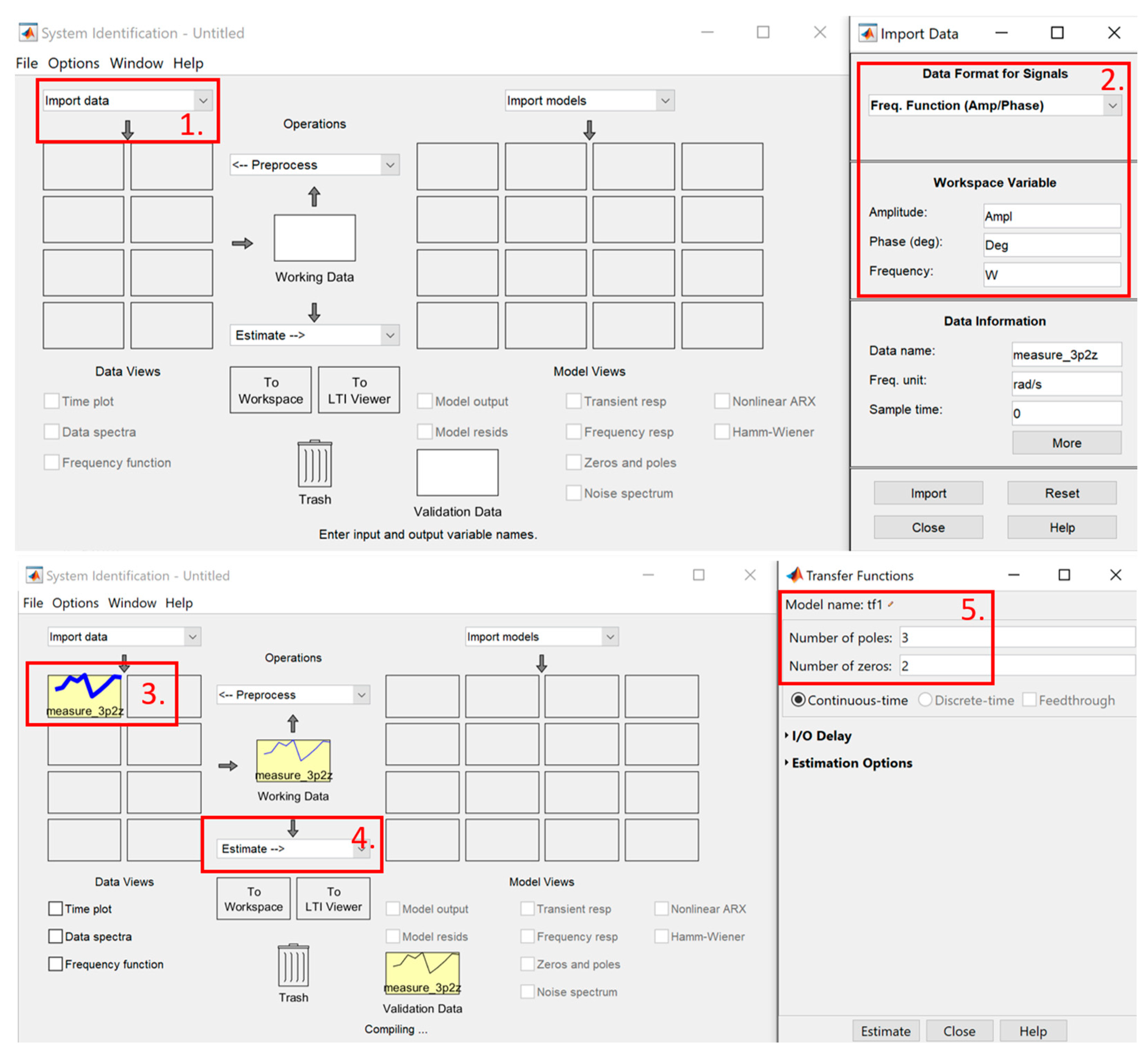
The captured data shown in
Figure 4 were converted to an idfrd (frequency response data) [
26] variable with the Matlab system identification toolbox shown in
Figure 5. This conversion was carried out with the import data function (1), and the frequency function (amp/phase) format was selected (2). The default frequency for this format is rad/s. Therefore, the imported frequency values were multiplied by 2π. The amplitude was converted from dB to a linear value. The obtained idfrd variable (3) was used to estimate the control transfer function using the system identification toolbox estimate transfer function model (4), which returned an idtf (transfer function model with identifiable parameters) variable [
26] as an output. In the estimation, the number of poles and zeros were defined (5). In this case, it was known that the number of poles was equal to three and the number of zeros was equal to two. These data resulted in an estimated control transfer function. Measured and estimated transfer function Bode plots for the feedback controller can be seen in
Figure 4. As can be seen, the measured curve follows the estimated curve without large deviations until 100 kHz, after which they differ substantially because of their proximity to the switching frequency, which distorts the experimental measurements. The estimated transfer function and the Bode plot were further used to develop a fast digital controller and verify the results using simulations. In a similar way, as a controller, the common DC–DC converter and the controller’s Bode plot were measured. Since the transfer function of the controller was known, as seen in
Figure 4, it was subtracted from the joint controller and converter Bode plot. As a result, a plot of the DC–DC converter could be obtained, as shown in
Figure 6. Comparing it to the calculated theoretical Bode plot, it is possible to see that they are close, but measurement is still preferable since it gives more accurate results.
One more method to obtain a Bode plot is to use simulation software to create a model of the converter. By injecting small signals in a wide range of frequencies, a Bode plot is obtained. The simulation model is shown in
Figure 7. In this case, Matlab Simulink was used to obtain the transfer function of the DC–DC converter. The control of the converter circuit was based on duty cycle control. To obtain the transfer function, a sinusoidal signal or an AC sweep was injected into the duty cycle. The frequency of the injected signal was variable. Therefore, by making relevant measurements in the output signal at the set parameters, the Bode plot was obtained.
Figure 7 shows that linear analysis points were placed at the duty cycle input of the PWM generator and the output voltage measurement point. In addition to the duty cycle signal, signal injection or input perturbation was performed. The measurement was taken after the converter had reached steady-state operation to remove noise from the converter’s switching transients.
The Bode plots obtained from the simulation model can be seen in
Figure 8. If a Bode plot differs from the experimentally measured one, the simulation model can be adjusted to fit the curves. Then, this adjusted model can be used for fine tuning. Based on the buck converter voltage plant described in Equation (4),
Rload is a variable and changing it will affect how the plant behaves. If the load is small in the case of larger resistance, the
Q will be larger, which will also make the double-pole loose phase quicker, and the phase margin will be worse, as can be seen in
Figure 8. As
Figure 8 shows, the difference between
Q = 1 and
Q = 10 is substantial. When the desired phase margin is set to be 60 degrees at a crossover frequency of around 50 kHz, it is not enough to shift the converter in the range of instability. When the same phase margin is used for a crossover frequency that is a little higher than the resonance point frequency, it may be enough to cause instability, and with this it can be concluded that the effect can be neglected if the converter controller is designed using the recommended phase margin of 45 or 60 degrees with a crossover frequency at least five times higher than the resonance point [
27].
3. Design of Analog Output Voltage Controller
Stability is very important in power converter design. In the first stages of converter design, stability criteria can be analyzed theoretically and based on simulations. Later, after the development of an experimental prototype, frequency response analyzers (FRAs) or the step response method can be used to estimate stability experimentally. Bode plots are the most used method to analyze converter stability [
28]. Further in this paper, this approach will be used to develop the fast voltage control loop of a DC–DC converter with digital control. Since the proposed method is based on an analog controller design method, an analog controller development process will be shown. Later, the results will be compared with those for a digital controller.
The type III compensator is the most widely used controller for DC–DC converters [
29]. It is more appropriate because of its higher phase boost compared to the type II compensator, which is needed at higher crossover frequencies. With a higher crossover frequency, the converter will respond faster to load changes [
30]. It is possible to achieve a high crossover frequency with analog control and this type of controller [
31]. There is also a limitation because the crossover frequency cannot be close to the switching frequency [
28]. Type III control is tuned using the k-factor method [
32], which allows the components of a controller to be calculated in an easy way. This method is widely used by engineers due to its relatively good performance and easy calculations. A type III analog controller can be implemented with an operational amplifier and a network of capacitors and resistors [
28]. A typical circuit of a type III analog controller can be seen in
Figure 9.
The passive components of the analog controller shown in
Figure 9 can be calculated using these equations [
28]:
The transfer function of the controller can be calculated as follows:
Resistors
R1 and
R4 are used to set the desired output voltage based on the reference voltage. Using Equations (5)–(12) and the buck converter voltage control transfer function described by Equation (13), it is possible to calculate the components of the controller and obtain the transfer function of the controller as follows:
The chosen crossover frequency in this case is 50 kHz, and the phase margin is 60°. After performing calculations with Equations (5) and (6), the necessary phase boost is 122°, and a gain of −14 dB is needed in order to achieve the desired response. After calculating the passive components, it is possible to obtain the transfer function in the Laplace domain using Equation (13). The obtained transfer function of the control plant is described by Equation (14) and it can be represented graphically using mathematical software. In this case, Matlab was used to obtain the frequency response of the analog controller, which can be seen in
Figure 10.
The type III control plant was combined with the buck voltage control transfer function, and an open-loop Bode plot of the converter and controller was obtained. This can also be carried out using Matlab by multiplying both the type III control and voltage plants. The obtained Bode plot can be seen in
Figure 11.
The formulas of the k-factor approach were changed to have frequencies instead of resistor and capacitor values, which are more suitable for digital control implementation [
32]:
Equations (15)–(19) also make it possible to calculate the limitations of control. For example, at a low crossover frequency, the required phase boost will be negative if the desired phase margin is set too low, which is impossible. These conditions will be used later in the analysis of the digital controller design.
When analyzing the stability criteria of the open-loop transfer function Bode plot shown in
Figure 11, the converter is stable because both of the following conditions are met: the phase margin is around 60 degrees, which is over 0°, and the cut-off frequency is around 50 kHz. To test the stability before practical testing, a Simulink simulation model with an analog controller was created. The simulation uses MOSFET switches to simulate the switching of the converter and uses other blocks like a PWM generator and a transfer function. This simulation model can be seen in
Figure 12. It can also be substituted with transfer functions, but then the switching of current and voltage cannot be seen. This results in faster simulations because there is no switching action to slow the simulation down and it is possible to obtain a step response quickly.
With the simulation model, it is possible to see how a change in load affects the transient response and how the phase margin affects the transient speed, stability, and overshoot/undershoot. In
Figure 13,
Figure 14,
Figure 15 and
Figure 16, phase margins of 30°, 45°, 60°, and 90° are compared (optimal values from [
33]) with the load resistor changing from 5 Ω to 2 Ω. It can be seen that the 60° phase margin gives a smaller undershoot than the 45° phase margin. The phase margin might be higher than 60° as well. In this case, the system is highly stable, but transient speed is lost because of the damped response. This can be seen in
Figure 13. Lower stability and a higher undershoot can be seen in
Figure 16 with a phase margin equal to 30°.
To implement an analog controller practically, an NCP1034 synchronous buck controller was used [
34] and it was implemented into experimental prototype of a DC–DC converter, as can be seen in
Figure 17. Following the recommendations given in the datasheet and calculations, the switching frequency was set to be 100 kHz. To avoid a discontinuous conduction mode, an inductor was chosen equal to 68 µH. The phase margin was set at 60° after analyzing
Figure 13,
Figure 14,
Figure 15 and
Figure 16.
The Bode plot of the combined analog type III controller and converter shown in
Figure 18 was measured using the frequency response analyzer shown in
Figure 3. The obtained data were used to estimate the transfer function of the controller and to estimate the combined transfer function with Matlab using a method described previously. The Bode plot shown in
Figure 18 indicates the stability of the converter, and it can be seen that the phase margin is close to 30°. This means that, theoretically, the step response should be similar to that of
Figure 16 and the converter should be stable.
From the experimental measurements, the controller transfer function was obtained. By comparing it to the theoretically calculated Bode plot of the controller that can be seen in
Figure 19, it is possible to see that they are close but not equal, which means that the passive components have slightly different values. Therefore, measurements are useful in this case as well.
Figure 20 shows an experimental converter response to a rapid load change. As can be seen, the transient process is as expected based on the theory. The converter response takes around 200 µs, but with a 100 kHz switching frequency, a type III controller, and a large inductance it is difficult to achieve significantly better results. Analysis of analog controller design will be used to develop a faster digital controller based on a similar approach but with included delays.
4. Analysis of Delays Introduced by Digital Control
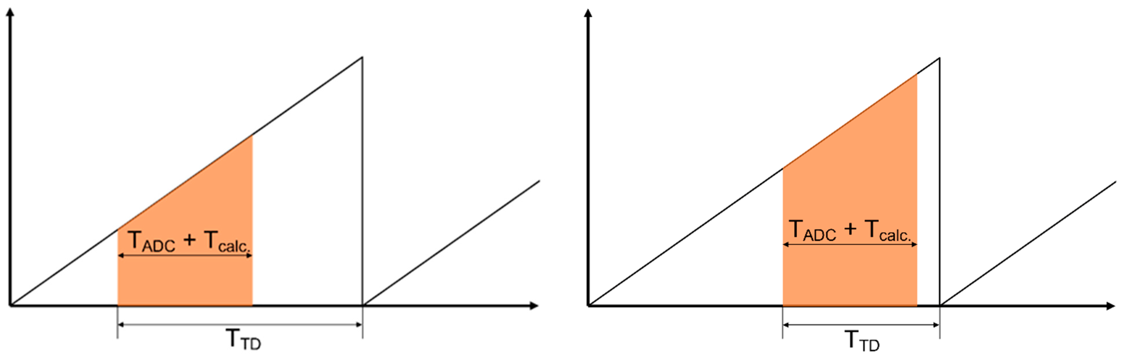
Transition from analog control to digital control has many advantages, like a smaller footprint, easier controller setup, and the possibility to change the control algorithm easily. However, the use of digital control also has several disadvantages such as unwanted delays that are caused by the discrete nature of the ADC and PWM and the time required for calculations. At low switching frequencies (below 50 kHz), digital control delays caused by the STM32G4 microprocessor are relatively minimal because multiple samples can be taken and multiple calculations can be performed in one switching period, and this results in analog control and digital control being very similar. At switching frequencies over 500 kHz, multiple samples cannot be taken, and multiple calculations cannot be performed in one switching period because of time limitations, which means that sampling delay and calculation delay affect the stability of the loop significantly. This means that there is a need to consider the phase degradation of a Bode plot that comes from zero-order hold (ZOH) and time delay (TD). These parameters are analyzed in Laplace form to determine how the conversion to a digital controller affects the phase at the crossover frequency. Knowing how much phase is lost is vital to converter stability and proper controller design. ZOH affects phase and gain, while time delay affects phase [
35]. Given that the crossover or cut-off frequency should be 5 to 10 times less than the switching frequency [
36], the lost gain from ZOH can be mitigated, so only phase loss is analyzed. ZOH in Laplace form is given by Equation (20), and time delay is given by Equation (21):
where
Tsw is the sample time or switching time, assuming one sample per time interval in seconds (s), and
TTD is the time from ADC sampling and calculation to the PWM period update.
Using the Euler formulas, it is possible to obtain the phase loss at a given crossover frequency caused by the digitalization of the control loop, and these values can be used for compensation of the control to achieve a similar response from the converter:
The
φZOH equation was simplified, and as a result Equation (25) [
37] could be obtained.
The phase loss variable (
was inserted in the phase boost formula for the k-factor method, and the equation was simplified as follows:
These delays can also be obtained graphically using Matlab or Wolfram software. Using Equations (20) and (21) of time delay and zero-order hold with known sampling times, the transfer functions were obtained. From these transfer functions, the delays were drawn graphically and are shown in
Figure 21 and
Figure 22. This approach is better compared to a simple calculation because it allows the visualization of how the delay affects the phase, and with it, it is possible to see that at higher frequencies it becomes even more challenging to compensate for this characteristic without changing how the sampling and calculations are performed.
A sample time of 1.2 µs for the time delay was calculated from tests with the STM32 microcontroller. Using a controller without optimized coefficients with an FMAC, an ADC, and an interrupt service routine (ISR) the delay for type III control was measured to be around 1 µs, which can be seen in
Figure 23. The measured value also includes the toggling of the output (GPIO) pin, which also adds some delay. This means that the delay is lower, but as a safety margin, 200 additional ns were added. At these high frequencies, even a small added calculation time can add unwanted delay. To achieve a better phase margin, the ADC and the calculation should be performed closer to the next PWM period. This can be set using the compare unit of the timer of the STM32 or another microcontroller. A visualization of this can be seen in
Figure 24. How ZOH affects the signal can be seen in
Figure 25. ZOH is set by sampling and calculation, and it serves as a constant comparison value for the counter until the next sample and calculation.
5. Design of Digital Controller
A stable digital controller of the converter could be designed with the previously used k-factor method for the type III controller using the obtained phase boost equation with delays included. The design of the controller was carried out in the Laplace s-domain, which was then converted to the z-domain. For the fast transient response, the desired crossover frequency was selected in a range from 50 kHz to 100 kHz. Increasing this frequency further was challenging since there was not enough phase boost to achieve the desired phase margin considering the analysis of the delays in the digital system. The equations for controller design were the same as those previously mentioned in the analog controller design section. At a 50 kHz crossover frequency using a time delay of 1.2 µs with a 500 kHz switching frequency, the calculated phase loss was 39.6°. This meant that to achieve a 60° phase margin, the phase boost needed to be 162.6°, which was already close to the limit. Changing to a 100 kHz crossover frequency with the same phase margin indicated that a 190.2° phase boost was needed, which was too much. This meant that the phase margin should be lowered, for example, to 45°. Control values could be obtained easily by creating a Matlab script, which included the measured buck converter voltage plant, from which the parameters could be read and used for k-factor tuning. The script also allowed the combined transfer function to be analyzed in cases where the phase crossed −180° before the set crossover frequency and indicated if a particular crossover frequency was possible to obtain with a given phase margin. The script ‘‘Matlab Code to Determine Transfer Function of the DC–DC Converter and Design Type III Controller ‘‘ is included in the
Supplementary Material S1.
After the controller calculation in the s-domain, it was converted to the z-domain using a bilinear transformation known as the Tustin or trapezoidal transformation [
38]. The reason for this conversion was to change from the frequency domain to a discrete-time system, which was appropriate for a digital converter. The bilinear transformation of the type III controller transfer function can be summarized by Equation (27) [
39]:
To implement this controller equation in a microcontroller, it should be changed to a linear equation as follows:
where a
1, a
2, a
3, b
0, b
1, b
2, and b
3 are coefficients of the digital controller; [n] is the measurement matrix; x is the input value array; and y is the output value array.
With the equations and coefficients obtained from the Matlab script, a simulation could be created to check the converter’s stability before moving on to practical tests. The simulation was configured in a hybrid mode where control was carried out using a discrete-time transfer function while the converter used a continuous time system. The simulation was similar to an analog control simulation. The only differences were that the control transfer function was in discrete time, as can be seen in
Figure 26, and there was an added time delay block. ZOH was added via a discrete transfer function block. Both simulations were used to compare the results. The analog control was set using data from the calculated s-domain values for digital control. In
Figure 27, these Bode plots are compared. It is possible to see that both of them are stable, and the delay is as expected.
While this simulation gives the expected results, there are a few blocks missing that prevent it from being implemented in a microcontroller. The practical converter also includes a resistor divider, quantization from an ADC, and a PWM counter value. All these values add an offset to the control, which needs to be compensated for it to retain performance, as can be seen in the simulation. In
Figure 28, it is possible to see how the actual microcontroller control looks as a block diagram. At the beginning, the voltage from the output is downscaled by a resistor divider, which is shown as the K
div block. The resistors are selected in such a way that at the maximum output voltage, which is 48 V, the divider output does not exceed 3.3 V. These resistors are 15 kΩ and 1 kΩ. This value can be calculated using Equation (29), which characterizes how much the output voltage decreases:
This value, which comes from a resistor divider, is then converted to a 12-bit value, which offers good resolution and a high speed. The resolution can be increased with oversampling, but that would slow down the ADC. The gain added by the ADC can be calculated using Equation (30) [
39], and its resolution can be calculated using Equation (31).
With these gains, the duty cycle output will be in a range from 0 to 1, but because the counter is used, additional gain needs to be added to normalize the value. An HRTIM is a counter that counts to a value of 2
16. This value depends on the needed frequency and the set counter value. For a PWM with a 500 kHz frequency with the highest possible resolution, a timer is set up with a maximum frequency of 5.44 GHz, which, divided by 500 kHz, results in a maximum counter value of 10,880, which can be seen in Equation (32). This value needs to be introduced in the calculation, and it results in gain, which is suitable for STM32 control. The overall equation for this gain is shown in Equation (33):
This gain is inserted into control Equation (27), which allows the following equation to be obtained:
With the calculated coefficients and control values, testing was carried out experimentally. The test was designed to check the stability of the converter when the start of the ADC sampling was shifted. The digital controller was not changed during this process, as can be seen in
Figure 29. A small shift closer to the start time introduced a phase margin change of almost 15°. While this was not enough to shift the converter into instability, it was enough to achieve an overshoot/undershoot that may be too high for the converter’s requirements, and this is why the tuning of such a solution is vital for converter stability. At a 500 kHz switching frequency, the limitations of the microprocessor started to appear. The time for control calculation approached the switching time, which meant that it was harder to implement without further and more difficult optimizations. Also, other functions were affected because the ISR took some of the switching period, which meant other tasks were stopped.
It is possible to see in
Figure 29 that the converter was stable. With the added TD compensation, it came close to the analog control, but there was a disadvantage, which was a slightly worse gain. An experimental prototype can be seen in
Figure 30. A universal GaN-based PCB with an STM32G4 microcontroller on it was connected to a modified previously described PCB with passive components and analog control on it. The analog control was disconnected and replaced with a digital one.
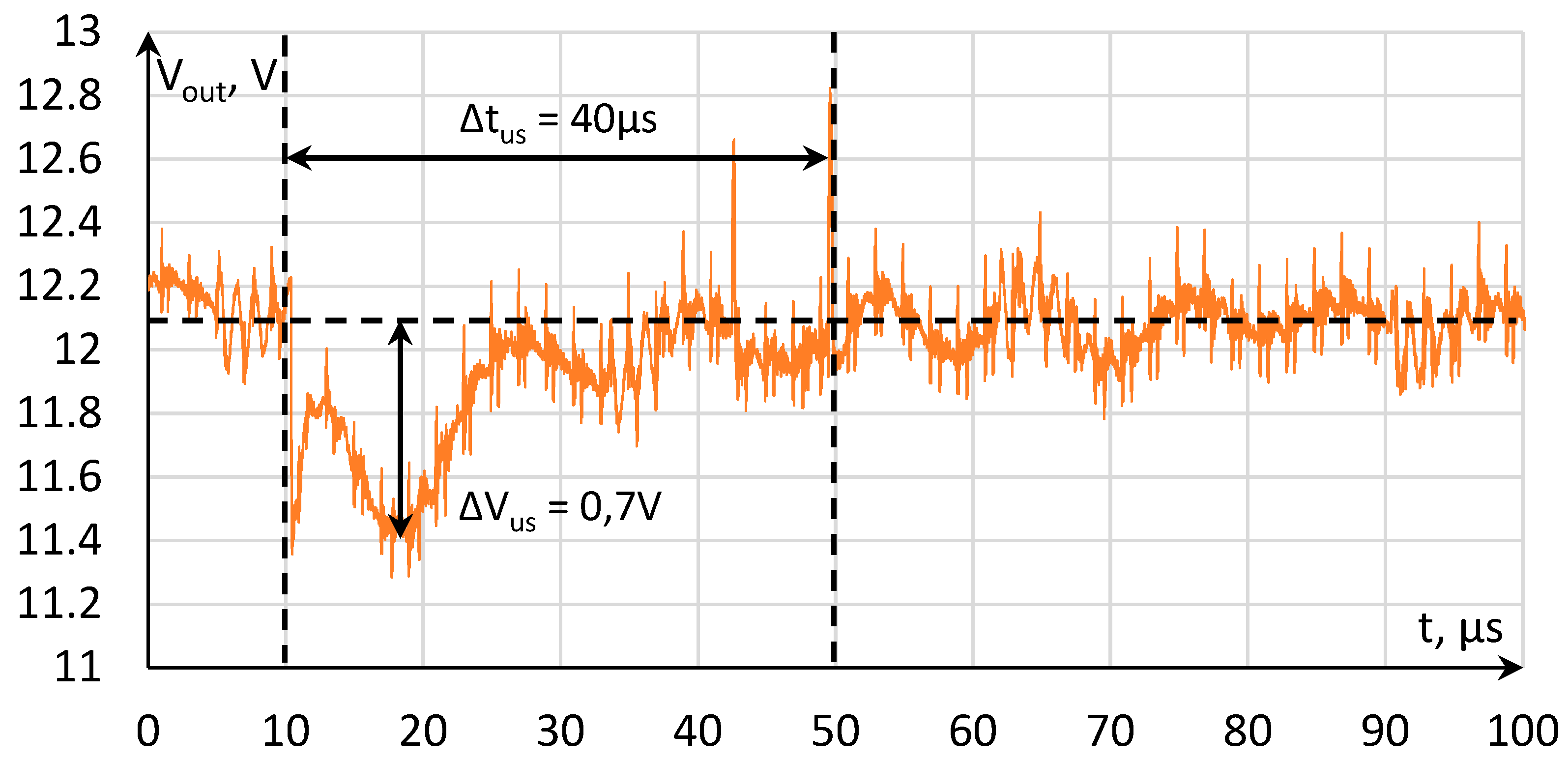
The experimental load test result can be seen in
Figure 31. It is possible to see that the transient time was close to 40 µs, although the digital control introduced 1.2 µs of time delay. The phase margin was close to 60°, which could be deduced by comparing this response to the previously measured simulation response and the Bode plot. The converter achieved stable control with a 500 kHz switching frequency using a 6 µH inductor and an 18.8 µF ceramic capacitor. These small values indicate it is possible to develop a high-power density converter. As can be seen in
Figure 31, the digital control achieved a 6% undershoot when switching the load from 5 Ω to 2 Ω. Comparing the practical results of the analog and digital control, it can be seen that the crossover frequency was higher for the digital control, making it five times faster. Further increases in bandwidth were challenging with this particular microcontroller since it was difficult to reduce the calculation and execution time further.
6. Conclusions
A GaN transistor-based DC–DC converter with a digital controller was developed, and the design process of the controller is analyzed in this paper. These transistors allow the switching frequency of the DC–DC converter to be increased, giving the possibility to select a lower inductor value and potentially improving the response time of the converter. Digital control is implemented by means of software, so it can easily be combined with other functionality, thus reducing expenses, by designing digital controller delays and the digital nature of the controller. These delays are analyzed in this paper, and they significantly impact the stability of the converter. This paper proposes the use of a type III controller as a digital controller, but the delays caused by the digitalization of the controller should be considered in the design process. This paper shows the step-by-step design processes for both analog and digital controllers.
This paper proposes a methodology for practical digital controller design based on analogy to traditional analog controller design. The design process of a controller consists of theoretical or experimental Bode plot acquisition. Experimental Bode plot acquisition requires the implementation of an initial controller and a frequency response analyzer. Further delays introduced by the digital controller are studied, thus obtaining the time delay dependency at different frequencies. The time delay at the desired cut-off frequency of the digital controller is added to the targeted phase margin, and then modified k-factor equations are used to calculate the locations of the poles and zeros of the controller. After the controller is calculated in the s-domain, it is converted to the z-domain using a bilinear transformation and is implemented in a microcontroller. Finally, the controller is implemented in a prototype, and stability is evaluated experimentally.
It was shown how much the calculation time impacts the phase of a controller’s Bode plot. These delays should be considered in the design of a digital controller. This paper shows adapted equations for controller calculations to achieve a desired bandwidth. Different possibilities to use simulation models to simplify controller development are shown in this paper. The obtained results were verified using an experimental prototype, and analog and digital controllers were implemented. The experimental results were compared with a theoretical analysis.
The converter achieved stable control with a 500 kHz switching frequency using an output filter with a 6 µH inductor and an 18.8 µF ceramic capacitor. Testing the digital control on an STM32G4 microcontroller introduced approximately 1.2 µs of time delay. As a result, a 50 kHz bandwidth was achieved at a 500 kHz switching frequency with the converter in voltage mode. The transient time, measured experimentally, was close to 40 µs, and the voltage undershoot was equal to 0.7 V with a phase margin close to 60°. If further bandwidth improvement is the goal, it could be challenging because of delays caused by the ADC and the calculations of the microcontroller, although GaN transistors could allow a higher switching frequency. The analog control converter’s transient time was around 200 µs, while the digital control transients took only 40 µs, making them five times faster. Such results can also be expected when analyzing practical and theoretical Bode plots: an analog control converter has a 10 kHz crossover frequency, but digital control has a 50 kHz crossover frequency. When seeking higher cut-off frequencies, discretization delays make it harder to achieve a good phase margin and time delays become important. The proposed method can be applied to other digital controllers and control loops to design controllers.


