
Frequency Modulation Scheme for CCM Boost PFC Converter to Improve THD in Light-Load Condition
Department of Electronic Engineering, Hanbat National University, Daejeon 34158, Republic of Korea
Electronics 2024, 13(2), 256; https://doi.org/10.3390/electronics13020256
Submission received: 3 November 2023
/
Revised: 19 December 2023
/
Accepted: 2 January 2024
/
Published: 5 January 2024
(This article belongs to the Topic Power Electronics Converters)
Abstract
:This study proposes a novel frequency modulation scheme for a continuous conduction mode (CCM) boost power factor correction (PFC) converter. The aim is to improve the total harmonic distortion (THD) under light-load conditions. Boost converters are widely utilized with CCM control for the PFC stage owing to their ability to achieve high efficiency with minimal components. In addition, they have a high power factor (PF) and low THD. However, despite being designed for CCM operation, the boost PFC converter transitions into discontinuous conduction mode (DCM) as the output load decreases. This mode, known as mixed conduction mode, degrades the PF and THD of the PFC converter. To address these issues, we propose a novel frequency modulation scheme. The CCM boost PFC converter adopts frequency variation to reduce the DCM region. To validate the feasibility of the proposed concept, a prototype with a 60 Hz/230 Vac input and 850 W/380 V output was utilized. Consequently, the boost PFC converter attains a high PF and low THD with simplified circuits.
1. Introduction
The increasing global power demand and growing concerns about its environmental impacts have prompted the introduction of regulations aimed at curbing this trend. Notably among these regulations are IEC 61000-3-2 and the Climate Saver Computing Initiative [1,2]. IEC 61000-3-2 particularly sets the limits on harmonic currents, which increases reactive power and causes a subsequent unnecessary increase in power capacity in grid systems as well as transmission line losses. To ensure low harmonic currents, a power factor correction (PFC) converter is necessary for power electronic systems. The PFC converter ensures a high power factor (PF) and low total harmonic distortion (THD) in power systems [3,4].
Examples of the PF and THD regulations utilized in computer power supplies are shown in Figure 1. The 80 PLUS certification serves as a benchmark for high-quality power supplies and offers four levels based on efficiency and PF. The highest level, titanium, demands an exceptionally high PF under 20–100% load conditions. Recently, this regulation has become more stringent, often requiring a very high PF even at a 20% load condition. In addition, IEC 61000-3-2 imposes limits on harmonic currents, effectively regulating the THD.
Among the various PFC converters, the boost PFC converter is widely utilized with continuous conduction mode (CCM) control owing to its high efficiency with a minimal number of components. In addition, it has a high PF and low THD compared with other PFC converters. However, although the boost converter is designed to operate with the CCM, when the output load is reduced in light-load conditions, the average inductor current is decreased and the inductor current starts to reach to 0 A. As a result, the CCM boost converter starts to operate with the DCM boost converter in light-load conditions. In particular, since the inductor current is small near the low input AC voltage, the DCM region occurs near 0 V of the input voltage. At that time, the inductor current still operates as the CCM near the peak of the input voltage. Therefore, the CCM and DCM regions both exist in the light-load condition. This is called mixed conduction mode (MCM), as shown in Figure 2a [5,6,7,8,9]. The problem with the MCM is that the DCM region makes current oscillations, as shown in Figure 2b, which degrades the PFC and THD [10,11,12,13,14,15,16,17].
Studies aimed at resolving these issues are underway [18,19,20,21,22]. In [20,21,22], various control techniques based on digital signal processing were proposed to alleviate THD concerns within MCM operation. These methods are highly effective and relatively easy to implement. However, digital integrated circuits (ICs) are more expensive compared with their analog counterparts and may be limited in terms of computational speed. In the absence of digital ICs, an alternative converter structure was introduced in [20] and [21] to enhance THD performance under light-load conditions. In [20], various snubbers were incorporated to suppress resonance between parasitic components. Although this approach improved the THD and PF, it introduced power losses within the snubber circuit. Consequently, Ref. [21] proposed a converter structure that maintained efficiency without degradation. This method eliminates the MCM operation by exclusively operating in CCM and DCM. Under heavy-load conditions, it operates in pure CCM operation and transitions to complete DCM operation as the output load decreases. This innovative approach harnesses the advantages of both CCM and DCM, resulting in a high PF and efficiency. However, implementing this method requires the addition of two extra thyristors and their associated gate signals, thereby increasing the complexity and cost of the system. In [22], the authors proposed a new controller structure to modulate the on-time of the PFC converter. By increasing the on-time of the converter near the peak current and decreasing the on-time near zero voltage, they improved the THD of the converter. However, this also required two additional switches, a resistor, a capacitor, and an amplifier to implement the proposed controller.
To resolve these challenges, this study presents a novel method to improve THD by utilizing simple passive components. The proposed method involves increasing the switching frequency near the zero-crossing point of the line voltage to minimize the DCM region. Further, it involves decreasing the switching frequency near the peak of the line voltage to reduce switching losses. This method relies on only a few components; thus, it offers a simple and versatile solution that is applicable to a wide range of analog ICs.
2. Concept of the Proposed Scheme
As shown in Figure 2, the CCM boost PFC operates with DCM when the average current of the boost inductor decreases compared with the ripple of the boost inductor. The boundaries between the CCM and DCM regions can be determined as follows:
where is the input current, is the current ripple of the inductor, Vline is the line voltage, Dswitch is the duty ratio of the switch, Lboost is the boost inductor, and fswitching is the switching frequency. Therefore, the DCM region decreases by increasing the switching frequency, resulting in improved THD and PF. However, although a high frequency improves the PF and THD, the frequency cannot be easily increased by the general power supply because it causes high switching losses at the switches. Thus, the proposed method adopts frequency modulation, as shown in Figure 3.
The proposed scheme utilizes a high switching frequency near the zero-crossing area to reduce the DCM region. Moreover, near the peak of the line voltage, a low switching frequency is employed to reduce switching losses at the switch. Consequently, compared with the conventional method that employs a constant frequency, the proposed converter has a reduced DCM region owing to the high switching frequency near the zero-crossing area. This leads to a high PF and low THD. In addition, the proposed converter utilizes a lower switching frequency compared with the conventional converter near the peak line voltage, thereby avoiding an increase in switching losses at the switch. Therefore, the proposed method enables the boost PFC converter to achieve a high PF and low THD without compromising efficiency. To validate the effectiveness of the proposed method, we varied the switching frequency from 40 to 80 kHz and compared it with the conventional boost PFC converter that operates at 60 kHz. Notably, the frequency variation can be modulated from 50 to 70 kHz or 30 to 90 kHz. However, the impact on the electromagnetic interference (EMI) filters at the input stage should be considered during frequency variations, as excessively low frequencies can affect these filters.
3. Implementation of the Proposed Scheme
The key concept of the proposed idea is to modulate the switching frequency along the input AC voltage. Therefore, in Section 3, the method to implement the proposed frequency modulation scheme is explained. Section 3.1 discusses the implementation method for the analog integrated circuit (IC) and Section 3.2 discusses the implementation method for the digital IC.
3.1. Implementation with Analog ICs
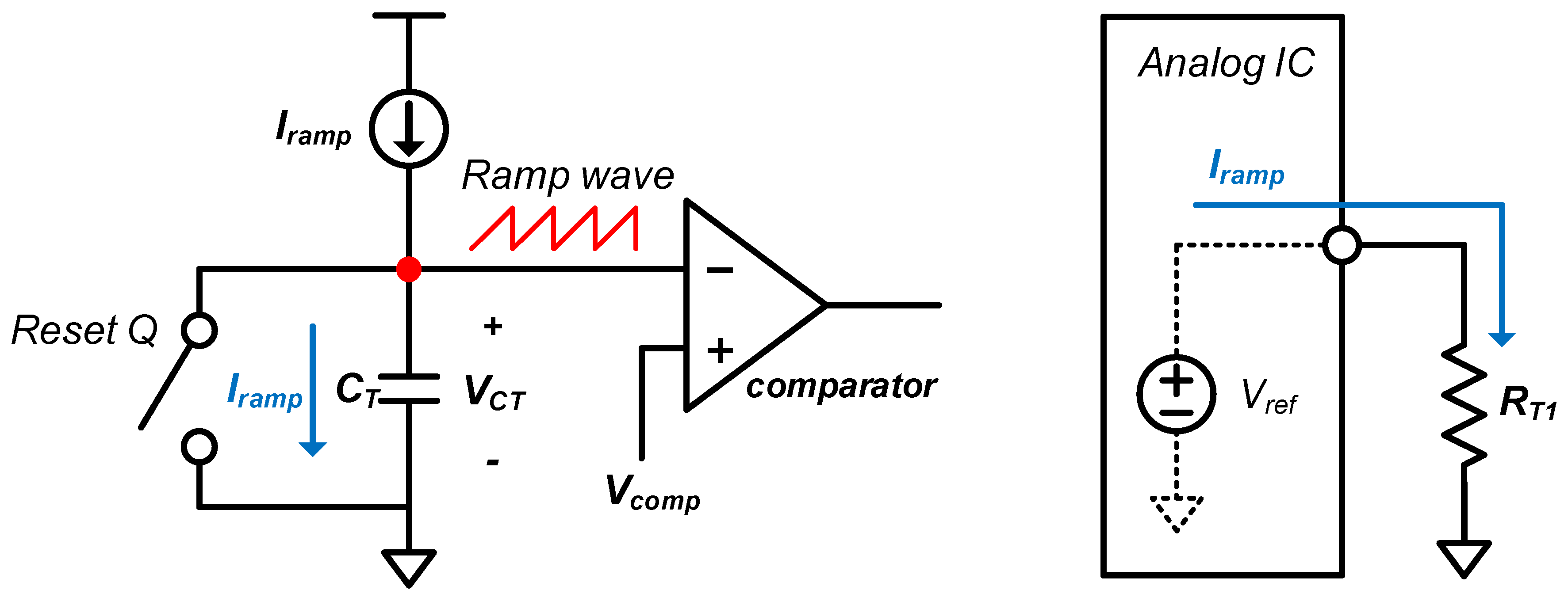
The switching frequency of the general analog IC is determined by the frequency of the ramp wave. The ramp wave represents the voltage of the timing capacitor CT, which increases when the ramp current Iramp flows through the timing capacitor, as shown in Figure 4. The ramp current is decided by the internal reference voltage and external resistor. Once the ramp voltage reaches a particular level, it is reset by utilizing a switch. Therefore, the frequency of the ramp wave varies with variations in the ramp current. In a general IC, as shown in the figure, the ramp current can be externally modulated with a reference voltage and RT to set the switching frequency. Therefore, to implement the proposed method, a line voltage adaptive lamp current is required.
Because the line voltage should be sensed in the boost PFC converter for feedback, the sensed AC voltage, VAC_det, is utilized to create a ramp current. Accordingly, the proposed method utilizes the line voltage, as shown in Figure 5, to modulate the ramp current. The value of VX varies with the line voltage as follows:
where Vref represents the internal reference voltage of the analog IC. The ramp current Iramp is calculated as follows:
Notably, the first term of the ramp current is constant. However, the second term varies with VX, which in turn varies with VAC_det. Because VX is at its maximum when the line voltage is at its peak, the ramp current reaches a minimum at the peak of the AC line. In addition, the ramp current reaches a maximum at zero voltage of the AC line. Consequently, the ramp current is modulated by utilizing simple passive components.
The major waveforms of the conventional boost PFC converter and proposed converter during MCM operation are shown in Figure 6. In the conventional converter, the switching frequency remains constant regardless of input voltage variations, resulting in a large DCM region. However, with the proposed frequency modulation scheme, the switching frequency varies with the line voltage. Because the switching frequency is higher near the zero-crossing area, the proposed converter has a reduced DCM region, which results in high PF and low THD. The full system with the Section 3.1 is attached in Appendix A.
3.2. Implementation with Digital ICs
One notable advantage of the proposed scheme is its implementation with both analog and digital ICs, such as digital signal processors (DSPs) and microcontroller units. Implementing the proposed scheme with digital ICs requires no additional components. This is because the sensing data required for the proposed scheme are already sensed by the digital IC for the feedback loop control. In contrast, the analog IC implementation described in Section 3.2 necessitates the utilization of the VAC_det signal and four resistors to generate the input voltage adaptive ramp signal. However, when employing a digital IC, only the VAC_det signal is required, and these data are utilized to generate variable frequencies.
For example, in the DSP manufactured by Texas Instruments, the frequency of the pulse-width modulation (PWM) signal is set by the time-base period (TBPRD) register. Assuming a boost converter switching frequency of 60 kHz and a DSP clock frequency of 120 MHz, the TBPRD can be calculated as follows:
where fck and fsw are the clock and switching frequencies, respectively. Consequently, the TBPRD value was determined to be 2000. This value changed with the switching frequency or DSP speed. In a constant-frequency system, such as a conventional CCM boost PFC converter, the TBPRD value remains unchanged and is always set at 2000 for a system with switching and at clock frequencies of 60 kHz and 120 MHz, respectively. Only the time-base counter (TBCTR) varies to modulate the duty ratio.
TBPRD = fck/fsw
However, to implement the proposed frequency modulation scheme, the boost PFC converter should operate at a high frequency near the zero-crossing area of the input voltage and a low frequency near the peak of the input voltage. This means that the proposed converter should have a low TBPRD value near the zero voltage of the 60 Hz line voltage and a high TBPRD value near the peak voltage of the 60 Hz line voltage. Therefore, by modulating the TBPRD according to the 60 Hz line voltage, as shown in Figure 7, the switching frequency can be adjusted to operate with the proposed scheme.
To design the TBPRD shown in Figure 7, the sensed input voltage VAC_det was utilized to create a 60 Hz line voltage shape. We assumed that the sensed line voltage VAC_det is expressed as follows:
where is the modulation factor from the input to the ADC voltage of the DSP. If VAC_det is directly added to the conventional TBPRD value, the switching frequency changes to a negligible value. Because the scale of the TBPRD value is considerably larger than the ADC voltage, the modulation should be operated as follows:
where TBPRDAC is an additional TBPRD value to vary the TBPRD during the line cycle, is a modulation factor from the ADC voltage to the TBPRD. The shape of the TBPRDAC is similar to that of the input line voltage, and its value is determined by utilizing . For a slight variation in the switching frequency, can be designed with a small value. In this case, the change in the conventional TBPRD value was insignificant with the addition of the TBPRDAC. Thus, can be designed with a large value, provided the frequency can vary considerably.
However, directly adding the TBPRDAC to the conventional TBPRD value does not result in a proper operation because the value of the TBPRDAC is always positive throughout the line cycle. Consequently, this results in a decrease in the switching frequency compared with the conventional switching frequency. Therefore, a negative DC bias should be added simultaneously to the TBPRDAC. The DC bias is required to increase the switching frequency, and it is determined by calculating the difference between the nominal and maximum frequency, as follows:
where fconv is the conventional switching frequency and fmax is the maximum switching frequency near the zero voltage of the line input. The value is determined by the frequency range. Thus, its description is similar to that of Equation (6) as follows:
where fmin is the minimum switching frequency at the peak of the line input.
Therefore, the TBPRD of the proposed scheme can be calculated by utilizing Equations (4)–(8) as follows:
Assuming the target frequency ranges are from 40 kHz to 80 kHz, the TBPRDprop is determined to be 1500∙sin(wt) + 1500 based on Equation (9). Therefore, the TBPRD value of the proposed converter varies from 1500 to 3000, resulting in frequency variation between 40 kHz and 80 kHz based on Equation (4) with a 120 MHz clock frequency.
3.3. Simulation Results
The key waveforms of the proposed frequency modulation scheme are shown in Figure 8. In the conventional boost PFC converter, which is the left figure, the ramp current is constant, and the frequency of the ramp voltage is also constant. On the other hand, the proposed boost PFC converter, shown in the right figure, has variable ramp current by using the input voltage to make the ramp current. As a result, the proposed converter has a lower frequency near the high input voltage and a higher frequency near the zero voltage. Since the switching frequency cannot be observed during the 60 Hz input frequency, the input voltage is adjusted to a relatively high frequency to see the switching frequency.
4. Experimental Results
The effectiveness and feasibility of the proposed frequency modulation scheme were validated by utilizing a 60 Hz/230 Vac input and 850 W/380 V output prototypes. Generally, the CCM boost PFC converter operates at a relatively low switching frequency owing to its inability to achieve zero-voltage switching during CCM operation. Therefore, the general CCM boost PFC converter operates near 60 kHz, so the center-switching frequency of the proposed converter was designed to be 60 kHz. The frequency varied from approximately 40 kHz to 80 kHz. The frequency range can be modulated by utilizing four resistor values in the analog IC or by calculating the value for the digital IC. In this experiment, we compared the proposed boost PFC converter with a conventional CCM boost PFC converter with analog control prototypes.
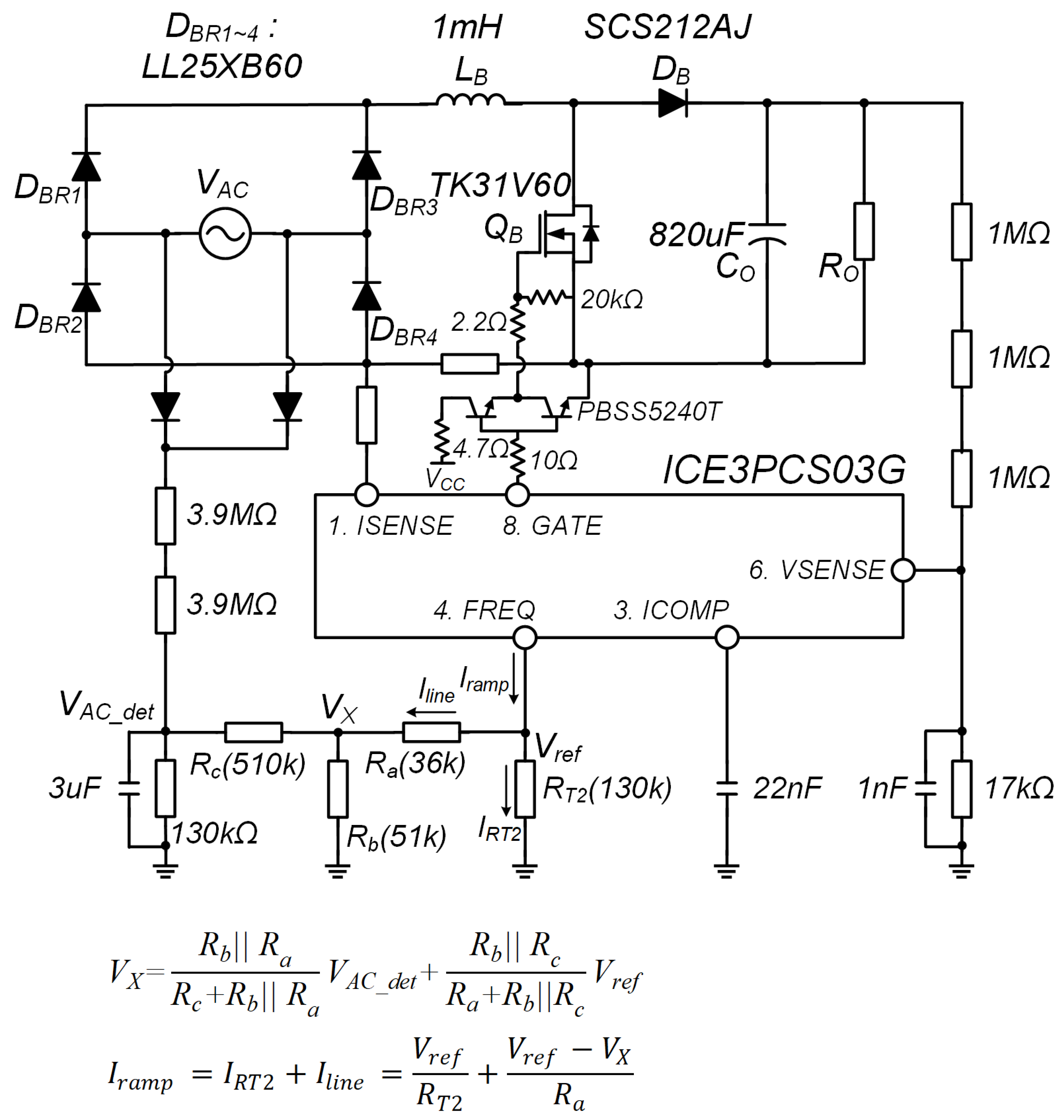
The experimental specifications and design examples of the prototype converters are listed in Table 1. As previously mentioned, both topologies are based on the CCM boost PFC converter. The proposed converter incorporates a frequency modulation scheme to reduce the DCM region under light-load conditions. The target application of this converter is a server power supply because the power supply for data centers is subject to strict regulations owing to its high power consumption and reliability. Therefore, achieving high efficiency, high PF, and low THD is crucial and a challenging objective for a server power supply. The input voltage for the experiment was 220 Vac/60 Hz, corresponding to a high line voltage. This voltage was converted to 380 VDC by utilizing a boost converter. The output power was set at 850 W. To implement the CCM boost PFC converter, we utilized the widely used Infineon ICE3PCS03G [23], which offers various subfunctions and facilitates easy designs. However, it operates at a constant switching frequency. Although ICE3PCS03G is designed for CCM control using four resistors and the sensed input voltage VAC_det, it can also operate with frequency modulation control. For the proposed converter, we applied external resistors Ra, Rb, Rc, and RT using small 1608 chip resistors with values of 36 kΩ, 51 kΩ, 510 kΩ, and 130 kΩ, respectively, as per Equation (2). By utilizing these resistors, the proposed converter could operate within a frequency range of 40 to 80 kHz. To compare the performance, the conventional CCM boost PFC converter was tested at switching frequencies of 40, 60, and 80 kHz.
The testbed for the prototype converters is shown in Figure 9. To ensure precise measurement of the PF and THD, a Yokogawa WT3000 power analyzer [24] was utilized. This power analyzer boasts an exceptional accuracy of 0.02%. In addition, it offers a bandwidth range from 0.1 Hz to 1 MHz for PF and THD measurements. The output power was measured by utilizing a Yokogawa WT1600 power analyzer [25].
Figure 10 and Figure 11 show key waveforms of both prototype converters at a 20% load condition. Although both converters are designed to operate with CCM, they operate with MCM operation in light-load conditions. Since the PFC converters are designed to operate with CCM over a 50% load condition, they start to operate with DCM under a 50% load condition. And because the advantage of the proposed frequency modulation scheme is to decrease the DCM region in MCM operation, the effectiveness of the proposed converter is analyzed by focusing on the light load such as a 20% load condition. For both figures, the yellow line is a 60 Hz input high line voltage with 220 VAC, and the blue line is a current waveform of the boost inductor. Since the switching frequency of the boost converter is relatively high compared to the 60 Hz line frequency, it is shown as a ripple current shape. Lastly, the red line is an input current waveform flowing between rectifier diodes and an input capacitor of the boost converter. Since there is an input capacitor between the boost converter and the rectifier diodes, the input current can be a clear sine wave even though the inductor current has a large ripple current. And the input current near zero-crossing has a small discrete current due to the dead zone.
As shown in Figure 10, the conventional boost PFC converter has a DCM region owing to the low-output power condition. The width of the DCM region increases as the output power decreases. In particular, under the 20% load condition, the DCM region occupies approximately 56% of the line cycle, whereas the CCM region occupies approximately 44%. Determining the inductor current from the waveform is challenging as it is filtered by the input capacitor between the rectifier diodes and boost inductor. However, precise measurement is possible by utilizing the WT3000 power analyzer. In the DCM region, numerous suboscillations caused by resonances between parasitic components occur, resulting in a decrease in the average value of the input current. Consequently, distortions in the input current are observed and represented as a red line in the measurement. As shown in the figure, the conventional CCM boost PFC converter has a THD value of 9.51% at a load condition of 20%. This value is quite low because the THD generally increases under light-load conditions. However, owing to the stringent THD regulations for server power supplies, even under light-load conditions, this value is considered significant. This is particularly relevant as data centers often operate under light-load conditions.
Compared with the conventional system, the proposed converter in Figure 11 shows a considerably lower DCM region under the same output load condition. Because the switching frequency is increased near zero voltage, ripple currents are reduced compared with the conventional boost converter, and the DCM region decreases from 56% to 42%, representing a 25% reduction. On the other hand, the ripple current near the peak voltage increases from 1 A to 1.5 A due to low switching frequency. Therefore, the proposed converter achieved high-quality current through the implementation of a novel frequency modulation scheme.
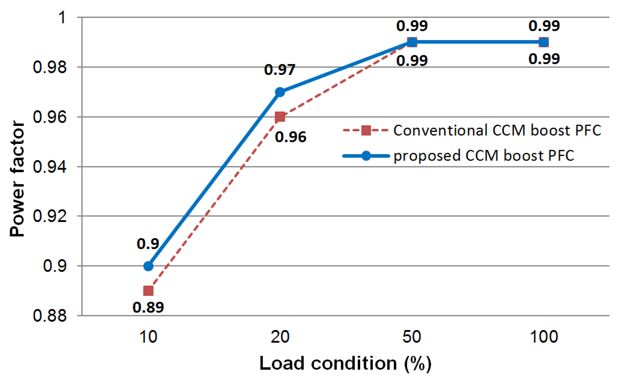
The measured THD values of both converters under all load conditions are shown in Figure 12. Notably, the proposed converter showed no improvements at heavy loads, as the THD remained consistently low. However, as the output load decreased, the DCM region increased, resulting in a significant increase in the THD. In practice, because the THD is generally low under heavy-load conditions, the key to satisfying various regulations is to have a low THD under light-load conditions. The advantages of the proposed converter are significant under light-load conditions.
The measured PF values of the prototypes are shown in Figure 13. In general, the value of the PF is high under heavy-load conditions, similar to the THD. However, as the output load decreases, the PF starts decreasing as well. The main reason for the decrease in the light-load condition is related to the phase-leading current in the input capacitor. This current, with a different phase from the input voltage, predominantly degrades the PF. Notably, the absolute value of the phase-leading current remained constant regardless of the output load condition; thus, it significantly influenced the PF under light-load conditions. Therefore, the proposed scheme does not yield a considerable improvement in the PF, as the low PF under light-load conditions is not related to the DCM region. However, the PF consists of a displacement and distortion factor. Therefore, improving the THD has a positive effect on achieving a high PF. As a result, the PF of the proposed converter was slightly improved under light-load conditions.
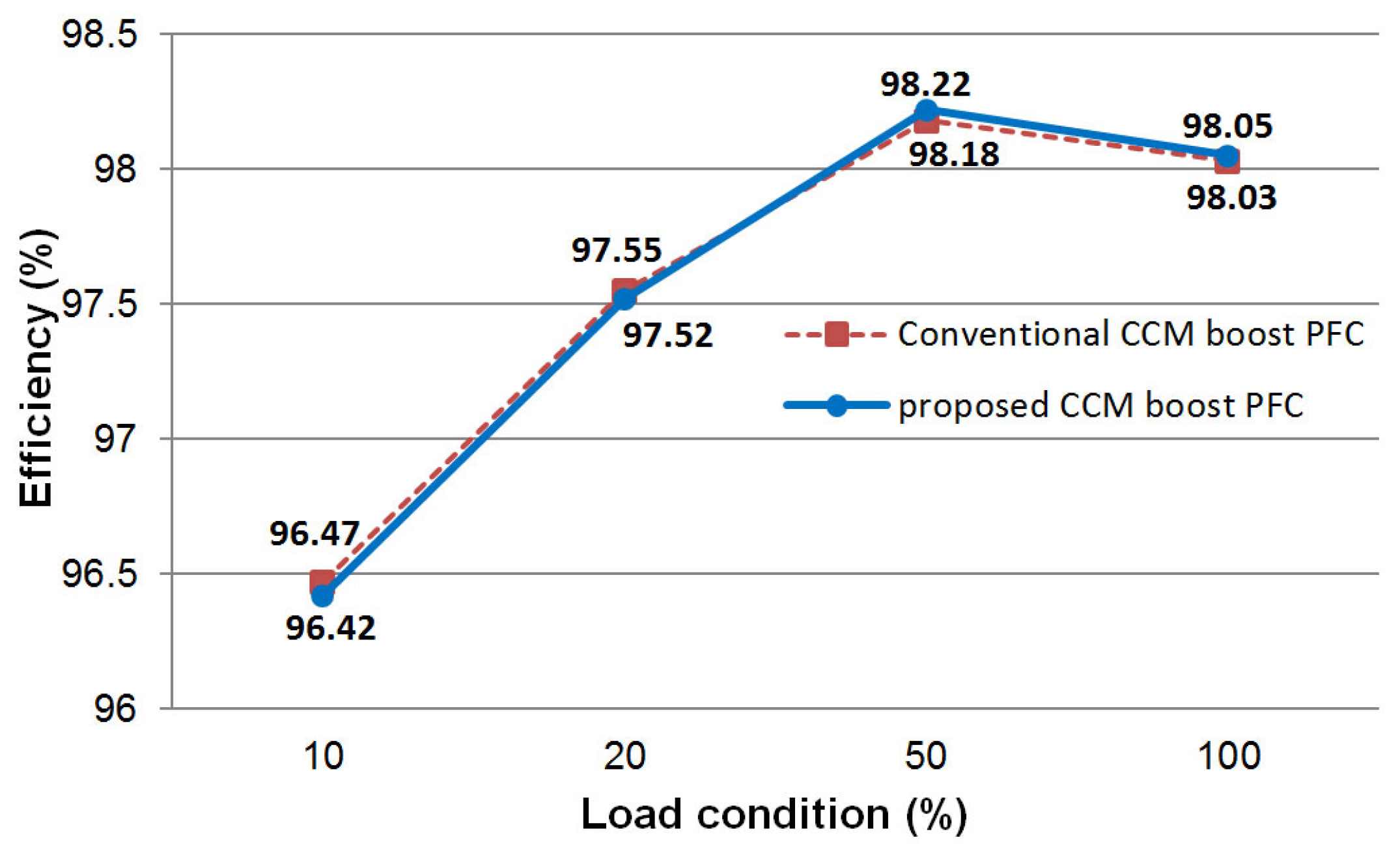
The measured efficiencies of both prototype converters are shown in Figure 14. Although the proposed converter operated at a high switching frequency to reduce the DCM region, it did not degrade the efficiency under all load conditions. This is because the proposed converter reduced the switching frequency near the peak of the input line voltage. Therefore, the proposed converter improved the PF and THD without degrading efficiency.
5. Conclusions
This study proposed a simple method to improve the THD of a CCM boost PFC converter under light-load conditions by utilizing a frequency modulation scheme. Achieving a high PF and low THD is crucial in numerous applications, particularly in server power supplies. A low PF and high THD increase the reactive power, which increases conduction loss in transmission lines. Therefore, many industrial regulations strictly govern the PF and THD. The PFC stage, which typically employs a CCM boost converter, determines the PF and THD in a power system. The CCM boost PFC converter is an excellent choice for the PFC stage owing to its simplicity, fewer number of components, and high efficiency. In addition, it has a relatively high PF and low THD compared with other PFC converters with other topologies, such as buck or buck–boost converters. However, despite its excellent performance, as technology advances and regulations become more stringent, novel methodologies must be developed to satisfy these requirements. Many related studies have been conducted to improve the power quality using various concepts. The methods employed in previous studies have proven to be highly effective in enhancing power quality. However, owing to this trade-off, some decrease the efficiency of the system, whereas others require numerous components, such as MOSFETs, resulting in an increase in cost and volume. In addition, the utilization of active components degrades the reliability of power systems. Consequently, the practical application of many of these studies to industrial products has been challenging. However, the proposed method offers a distinct advantage. While it did not significantly improve the power quality, it clearly decreased the THD and enhanced the PF through the utilization of simple passive components. In addition, frequency modulation did not degrade the overall efficiency under all load conditions, although it increased the switching frequency near zero voltage. This highlights the paramount importance of the proposed method, which prioritizes practicality and reliability through a straightforward approach. Furthermore, the proposed method can be applied to almost all analog and digital ICs. The proposed control method emerges as a strong contender for numerous applications in which THD and PFC are crucial.
Funding
This research was supported by the “Regional Innovation Strategy (RIS)” through the National Research Foundation of Korea (NRF), funded by the Ministry of Education (MOE) (2021RIS-004) and MSIT (Ministry of Science and ICT), Korea, under the ICAN (ICT Challenge and Advanced Network of HRD) program (IITP-2023-00156212), supervised by the IITP (Institute of Information and Communications Technology Planning and Evaluation).
Data Availability Statement
Derived data supporting the findings of this study are available from the author on request.
Conflicts of Interest
The author declares no conflicts of interest.
Appendix A
Figure A1 is the total system and control structure of the proposed frequency modulated CCM boost PFC converter based on ICE3PCS03G IC.
Figure A1.
Total system structure of the proposed CCM boost PFC converter.

References
- IEC 61000-3-2; Limits for Harmonic Current Emissions (Equipment Input Current <16A per Phase). International Electrotechnical Commission: Geneva, Switzerland, 2001.
- Climate Savers Computing Initiative (CSCS). Available online: https://www.greenit.fr/climate-savers-computing/ (accessed on 1 January 2024).
- Kim, Y.S.; Sung, W.Y.; Lee, B.K. Comparative Performance Aanlysis of High Density and Efficiency PFC Topologies. IEEE Trans. Power Electron. 2014, 29, 2666–2679. [Google Scholar] [CrossRef]
- Lim, S.F.; Khambadkone, A.M. A Simple Digital DCM Control Scheme for Boost PFC Operating in Both CCM and DCM. IEEE Trans. Ind. Appl. 2011, 47, 1802–1812. [Google Scholar] [CrossRef]
- Van de Sype, D.M.; De Gusseme, K.; Van den Bossche, A.P.; Melkbeek, J.A. Duty-Ratio Feedforward for Digitally Controlled Boost PFC Converters. IEEE Trans. Ind. Electron. 2005, 52, 108–115. [Google Scholar] [CrossRef]
- Roggia, L.; Beltrame, F.; Baggio, J.E.; Pinheiro, J.R. Digital current controllers applied to the boost power factor correction converter with load variation. IET Power Electron. 2012, 5, 532–541. [Google Scholar] [CrossRef]
- Huber, L.; Jang, Y.; Jovanovic, M.M. Performance Evaluation of Bridgeless PFC Boost Rectifiers. IEEE Trans. Power Electron. 2008, 23, 1381–1390. [Google Scholar] [CrossRef]
- Clark, C.W.; Eberle, W.; Musavi, F. An adaptive digital controller for the mixed conduction mode boost power factor correction converter. In Proceedings of the 2013 Twenty-Eighth Annual IEEE Applied Power Electronics Conference and Exposition (APEC), Long Beach, CA, USA, 17–21 March 2013; pp. 2712–2719. [Google Scholar]
- Agorreta, J.L.; Reinaldos, L.; Gonzalez, R.; Borrega, M.; Balda, J.; Marroyo, L. Fuzzy Switching Technique Applied to PWM Boost Converter Operating in Mixed Conduction Mode for PV Systems. IEEE Trans. Ind. Electron. 2009, 56, 4363–4373. [Google Scholar] [CrossRef]
- Sebastian, J.; Cobos, J.A.; Lopera, J.M.; Uceda, J. The Determination of the Boundaries Between Continuous and Discontinuous Conduction Modes in PWM DC-to-DC Converters Used as Power Factor Preregulators. IEEE Trans. Power Electron. 1995, 10, 574–582. [Google Scholar] [CrossRef]
- Liou, C.Y.; Chieh, H.C.; Liou, W.R. Design and Implementation of a Boost Power Factor Correction Stage Operated in Mixed-Conduction Mode. In Proceedings of the 2011 International Conference on Electric Information and Control Engineering, Wuhan, China, 15–17 April 2011; pp. 2069–2072. [Google Scholar]
- Clark, C.W.; Musavi, F.; Eberle, W. Digital DCM Detection and Mixed Conduction Mode Control for Boost PFC Converters. IEEE Trans. Power Electron. 2014, 29, 347–355. [Google Scholar] [CrossRef]
- Tripathi, R.K.; Das, S.P.; Dubey, G.K. Mixed-Mode Operation of Boost Switch-Mode Rectifier for Wide Range of Load Variations. IEEE Trans. Power Electron. 2002, 17, 999–1009. [Google Scholar] [CrossRef]
- De Gusseme, K.; Van de Sype, D.M.; Van den Bossche, A.P.; Melkbeek, J.A. Digitally Controlled Boost Power-Factor-Correction Converters Operating in Both Continuous and Discontinuous Conduction Mode. IEEE Trans. Ind. Electron. 2005, 52, 88–97. [Google Scholar] [CrossRef]
- Cimini, G.; Ippoliti, G.; Orlando, G.; Pirro, M. Sensorless Power Factor Control for Mixed Conduction Mode Boost Converter Using Passivity-Based Control. IET Power Electron. 2013, 7, 2988–2995. [Google Scholar] [CrossRef]
- Juan, Y.L. Single switch three-phase ac to dc converter with reduced voltage stress and current total harmonic distortion. IET Power Electron. 2014, 7, 1121–1126. [Google Scholar] [CrossRef]
- Zodape, M.S.; Kamat, V.N. Use of Smart Metering for Resolving Harmonic Issues. In Proceedings of the 2016 International Conference on Electrical, Electronics, and Optimization Techniques (ICEEOT), Chennai, India, 3–5 March 2016; pp. 3961–3964. [Google Scholar]
- Clark, C.; Eberle, W.; Musavi, F. A DSP-based Zero Current and Discontinuous Conduction Mode Detection Method. In Proceedings of the 2013 IEEE Transportation Electrification Conference and Expo (ITEC), Detroit, MI, USA, 16–19 June 2013; pp. 1–5. [Google Scholar]
- Lopez, V.M.; Azcondo, F.J.; Castro, A.D.; Zane, R. Universal Digital Controller for Boost CCM Power Factor Correction Stages Based on Current Rebuilding Concept. IEEE Trans. Power Electron. 2014, 29, 3818–3829. [Google Scholar] [CrossRef]
- De Gusseme, K.; Van de Sype, D.M.; Van den Bossche, A.P.; Melkbeek, J.A. Input-Current Distortion of CCM Boost PFC Converters Operated in DCM. IEEE Trans. Ind. Electron. 2007, 54, 858–865. [Google Scholar] [CrossRef]
- Ghosh, R.; Narayanan, G. A Single-Phase Boost Rectifier System for Wide Range of Load Variations. IEEE Trans. Power Electron. 2007, 22, 470–479. [Google Scholar] [CrossRef]
- Zhao, C.; Zhang, J.; Wu, X. An Improved Variable On-Time Control Strategy for a CRM Flyback PFC Converter. IEEE Trans. Power Electron. 2017, 32, 915–919. [Google Scholar] [CrossRef]
- ICE3PCS03G. Available online: https://www.infineon.com/cms/en/product/power/ac-dc-power-conversion/ac-dc-pwm-pfc-controller/pfc-ccm-continuous-conduction-mode-ics/ice3pcs03g/ (accessed on 1 January 2024).
- Yokogawa WT3000. Available online: https://www.yokogawa.com/kr/library/resources/yokogawa-technical-reports/wt3000-precision-power-analyzer/ (accessed on 1 January 2024).
- Yokogawa WT1600. Available online: https://www.yokogawa.com/kr/library/resources/yokogawa-technical-reports/wt1600-digital-power-meter/ (accessed on 1 January 2024).
Figure 1.
Regulations of PF and THD for computer power supplies.

Figure 2.
Current waveforms of the boost PFC converter. (a) Current shape during MCM operation. (b) Current oscillation during DCM operation.
Figure 2.
Current waveforms of the boost PFC converter. (a) Current shape during MCM operation. (b) Current oscillation during DCM operation.

Figure 3.
Key waveforms of the proposed scheme.

Figure 4.
Frequency design method for general ICs.

Figure 5.
Design of line voltage adaptive lamp current.

Figure 6.
Comparison between the conventional and proposed boost PFC converter.

Figure 7.
Concept of the TBPRD modulation for the proposed boost PFC converter.

Figure 8.
Simulation results of the both converters.

Figure 9.
Experiment set-up of the proposed converter.

Figure 10.
Key waveforms of the conventional boost PFC converter at a 20% load condition.

Figure 11.
Key waveforms of the proposed boost PFC converter at a 20% load condition.

Figure 12.
Measured THD of the prototype converters under all load conditions.

Figure 13.
Measured PF of prototype converters under all load conditions.

Figure 14.
Measured efficiencies of the prototype converters under all load conditions.


Table 1.
Specifications and design examples of the prototype converters.
| Conventional Converters | Proposed Converter | |
|---|---|---|
| Target application | Server power supply | |
| Input voltage | 220 Vac/60 Hz | |
| Output voltage | 380 VDC | |
| Output power | 850 W | |
| Topology | CCM boost PFC converter | |
| Control IC | ICE3PCS03G (Infineon CCM PFC controller) | |
| Bridge diode | LL25XB60 (600 V, 25 A, 0.87 VF) | |
| MOSFET | TK31V60X (600 V, 31 A, 0.078 Ω) | |
| Diode | SCS212AJ (650 V, 12 A, SiC) | |
| Inductor | 1 mH | |
| Output capacitor | 450VXT820MEFCSN30 × 55 (450 V, 820 uF) | |
| Switching frequency | 40, 60, 80 kHz | 40 kHz~80 kHz |
| Ra, Rb, Rc, RT | - | 36 k, 51 k, 510 k, 130 k |
| Input power analyzer | Yokogawa WT3000 (0.02% accuracy within 1 MHz) | |
| Output power analyzer | Yokogawa WT1600 (0.1% accuracy within 1 MHz) | |
Disclaimer/Publisher’s Note: The statements, opinions and data contained in all publications are solely those of the individual author(s) and contributor(s) and not of MDPI and/or the editor(s). MDPI and/or the editor(s) disclaim responsibility for any injury to people or property resulting from any ideas, methods, instructions or products referred to in the content. |
© 2024 by the author. Licensee MDPI, Basel, Switzerland. This article is an open access article distributed under the terms and conditions of the Creative Commons Attribution (CC BY) license (https://creativecommons.org/licenses/by/4.0/).
Share and Cite
MDPI and ACS Style
Han, J.-K. Frequency Modulation Scheme for CCM Boost PFC Converter to Improve THD in Light-Load Condition. Electronics 2024, 13, 256. https://doi.org/10.3390/electronics13020256
AMA Style
Han J-K. Frequency Modulation Scheme for CCM Boost PFC Converter to Improve THD in Light-Load Condition. Electronics. 2024; 13(2):256. https://doi.org/10.3390/electronics13020256
Chicago/Turabian StyleHan, Jung-Kyu. 2024. "Frequency Modulation Scheme for CCM Boost PFC Converter to Improve THD in Light-Load Condition" Electronics 13, no. 2: 256. https://doi.org/10.3390/electronics13020256
Note that from the first issue of 2016, this journal uses article numbers instead of page numbers. See further details here.