1. Introduction
Buildings requiring a guaranteed power supply are also subject to pressure to adapt to the requirements of climate policy [
1] and the European Green Deal [
2], and ensure high energy efficiency [
3]. Railway signal buildings are one of those that require a guaranteed power supply. They need a specific power supply method to ensure constant access to energy and railway traffic safety [
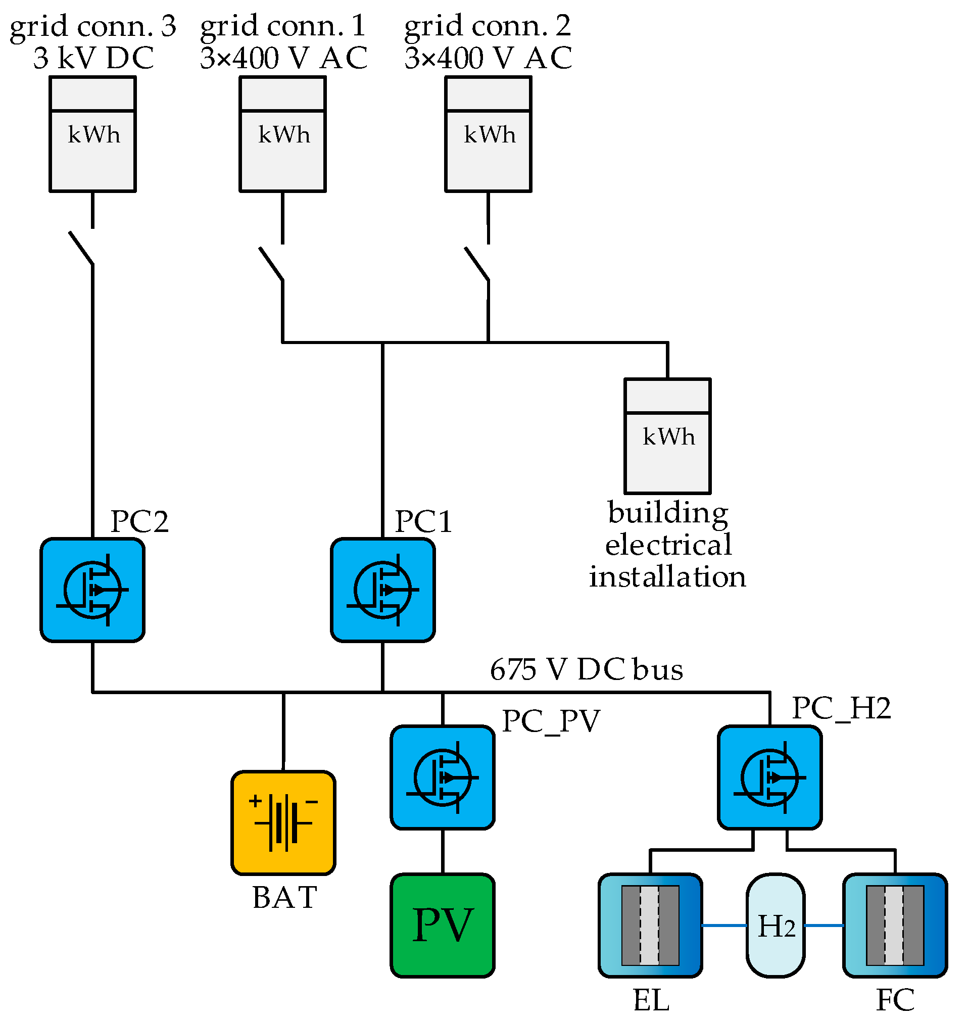
4]. The key is to provide two independent connections to the power grid, equipped with a guaranteed power supply system, most commonly consisting of a diesel generator set and a battery pack with inverters. The authors of the article are participating in a project aimed at constructing a complementary power system for railway signal buildings that will have a smaller carbon footprint and meet the technical requirements imposed by the Polish State Railways PKP PLK operator. The idea of the topology of the selected solution, which includes a few energy sources and power electronic converters, is shown in
Figure 1. The topology is characterised by a common 675 V dc-link voltage (battery pack voltage) to which different sources and additional energy storage are connected via the converters. In the proposed solution, the diesel generator set has been replaced with a hydrogen tank (additional energy storage) and a battery with increased capacity.
The main feature of the proposed power system structure with one common dc-link is the lack of a power converter for the battery pack and the presence of the bidirectional converter for hydrogen storage PC_H2 (the DAB converter). The direction of energy transfer in the PC_H2 converter depends on the selected operating mode. The chosen structure reduces the number of power converters, while the converters connected to the common dc-link must operate over a relatively wide range of voltage changes. The voltage in the dc-link depends on the state of charge of the battery pack. In the implemented project, a lithium iron phosphate (LFP) battery is used, for which the maximum voltage value of the LFP battery is assumed to be 3.6 V and the minimum voltage is 2.8 V [
5]. The voltage range of the applied battery is given later in the paper.
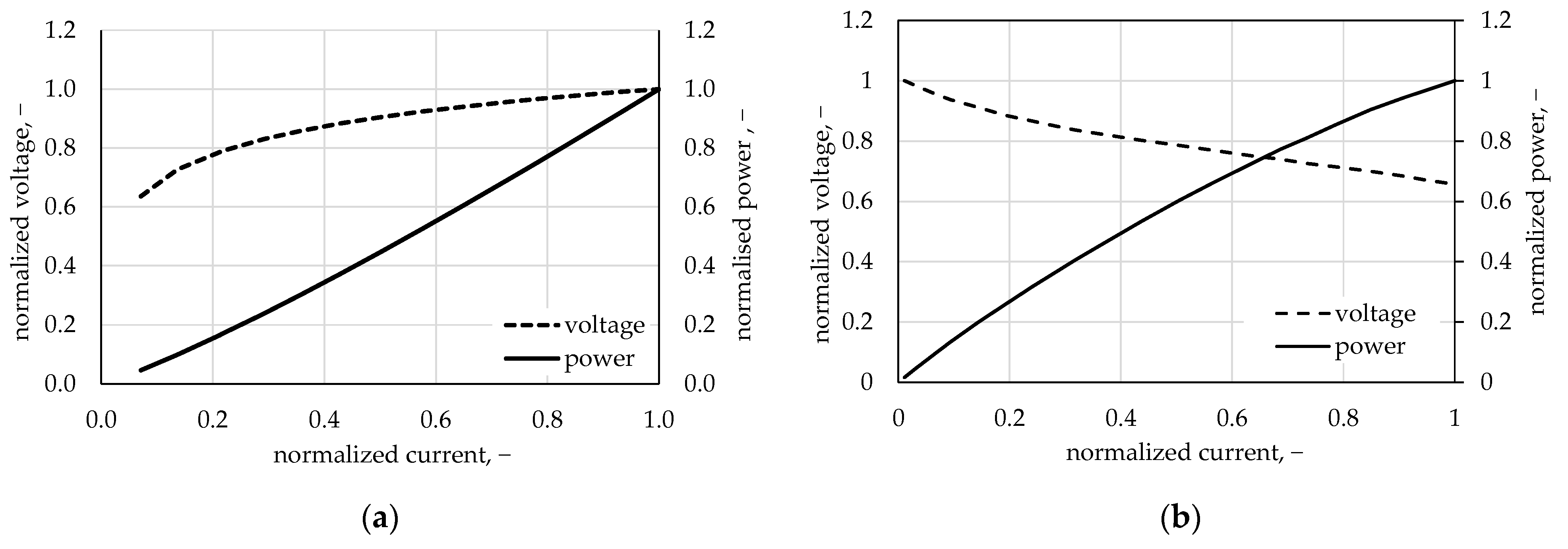
Two devices on the hydrogen storage side are connected to the PC_H2 converter: a fuel cell FC and a hydrogen generator EL. However, only one of them can operate at the same time. The characteristics of both devices are significantly different, with a notably wide voltage range in the useful part of the power output characteristics. The hydrogen flow generated by the hydrogen generator is linearly dependent on the supply current.
Figure 2a shows normalised characteristics of a PEM (Proton Exchange Membrane) hydrogen generator [
6], while normalised characteristics for a PEM fuel cell are shown in
Figure 2b [
7]. Similar to the generated hydrogen flow in the hydrogen generator, the electric power generated by the fuel cell is almost linearly dependent on the current (in the useful part of the characteristic). The next part of the article provides the voltage range from the hydrogen storage side.
Based on project assumptions, a 10 kW converter is needed as an interface between the battery pack and a fuel cell (or hydrogen generator). Both dc sources are characterised by a wide range of voltage changes. The selected LiFePO4 battery pack, 138 kWh, has a rated voltage of 691 V, and the output voltage varies from 561 V (minimal battery pack voltage) to 788 V (maximal battery pack voltage). The voltage on this side is assumed to range from 560 V to 790 V.
On the hydrogen tank side, a stack of fuel cells (serial/parallel connected) with a rated voltage of 170 V was assumed with the possibility of voltage change in the range of 60–100% (
Figure 2). An additional 10% of the range is added for safety reasons. Finally, it is chosen that for the fuel cell/hydrogen generator, the voltage can vary from 90 V to 190 V.
Under such conditions, the power electronic converter between the fuel cell/hydrogen generator and the battery storage needs to fulfil the demand for bidirectional energy flow and the need to ensure the proper output (battery side)/input (fuel cell side) voltage ratio. The development of distributed and renewable energy sources, and the need for energy storage, drives the development of DC–DC electronic converters. This trend is noticeable in current scientific publications. A particularly interesting converter for bidirectional energy flow is the Dual Active Bridge. The DAB converter is a DC–DC converter that consists of four main components: two transistor H-bridge converters, a transformer, and an inductor (
Figure 3). This converter allows bidirectional energy flow by controlling the phase shift between H-bridge converter gate signals [
8,
9]. The inductance value of the inductor
L1 limits the maximum power transferred through the converter. The inductor
L1 can be placed on the input (low voltage) or the output (high voltage) side of the transformer. It is decided to place the inductor on the output side due to its lower current value. This facilitates the design of the inductor, limits the number of high-current connectors on the low-voltage side, and reduces conduction losses inside the inductor winding.
The turns ratio of the transformer
n =
N2/
N1 determines the rated output-to-input voltage ratio of the converter. Considering voltage values in the middle of the described ranges (140 V and 675 V), it was decided to use a transformer with a turns ratio equal to 5. The DAB converter usually operates with a rated output-to-input voltage ratio or close to this operating point. Due to changes in the input (fuel cell) and output (battery) voltage levels, the designed converter should be able to operate with an output-to-input voltage ratio significantly different from 5 and ranging from 2.9 to 8.8. Such operation worsens the efficiency and increases the currents of the converter components due to the flow of reactive power on both sides of the converter [
10]. Considering reactive power during the design stage of the converter is very important.
The DAB converter is often used in applications with batteries interconnected to different voltage levels [
11,
12]. This converter is also used in electric car charging applications, and its bidirectionality is particularly useful for Grid-to-Vehicle and Vehicle-to-Grid applications [
13,
14]. Among other applications of the DAB converter are applications with fuel cells and hydrogen generators [
15,
16]. The DAB converter shows high efficiency, but only if the voltage is matched, i.e., when the voltages
VL and
VH meet the relation (
N2/
N1)
VL =
VH. In the case of voltage imbalance, other measures to improve the efficiency of systems are applied. In addition to the basic converter topology using two H-bridges and a single transformer, the literature includes studies of modified topologies. In [
17], the primary control method was combined with a structure using a transformer with variable leakage inductance and variable switching frequency. The unique design of the transformer made it possible to achieve higher efficiency for operation at low power. Another modification is inserting a blocking capacitor in series with the transformer winding [
18]. Combined with the revised control strategy, the operating region can be expanded to achieve greater efficiency.
The most commonly used control method for DAB converters is the single phase shift (SPS) method [
8,
9,
19]. In this method, the duty cycles for both H-bridges are equal to 0.5, and
vL and
vH converter voltages are square-wave. The phase shift between rectangular H-bridge voltages
vL and
vH is needed to control the energy flow. Other methods of power control with a higher number of degrees of freedom can be found, like EPS (Extended Phase Shift), DPS (Dual Phase Shift), and TPS (Triple Phase Shift) [
11]. The EPS method uses the inner phase shift of one H-bridge converter and the phase shift between voltages generated by H-bridges. In the DPS method, two inner phase shifts of both H-bridges (with the same value) are used together with the phase shift between voltages generated by converters. In the TPS method, both inner phase shifts are used independently, together with the phase shift between voltages generated by converters.
The issue with ensuring zero voltage switching ZVS in case of voltage changes is presented in [
8]. Two versions of the EPS method have been implemented in [
20] to increase the range of ZVS switching in the DAB converter.
Control methods like EPS, DPS, and TPS are also used to reduce backflow power (reactive power) caused by voltage mismatch. In [
21], an improved version of the EPS method, optimised based on the Lagrange method, has been investigated. The results show the possibility for good backflow power suppression but with a quite complicated computation of the duty cycle. The use of the DPS method is presented in [
22]. In this paper, the determination of phase shifts that minimise peak current has been proposed. The TPS method used for DAB converter control can be found in [
11,
23,
24,
25]. In [
23], values of phase shifts in the TPS method were first optimised using the finite control set (FCS) method using a converter model, and implemented using look-up tables. In [
24], TPS phase shift selection for minimum current stress was performed using AI methods. The neural network NN controller for mode of operation selection in the TPS method is also implemented in [
10]. Other methods, based on the converter model and the use of particle swarm optimisation with its implementation using TPS, can be found in [
25].
In [
26], other types of modulation (called triangular and trapezoidal) can be found. These modulations can increase efficiency but need much higher computation complexity.
Finally, it can be seen that more sophisticated control methods give good results but need deep knowledge of all component parameters used in the converter and require considerable computational effort to achieve the assumed goal.
The paper deals with the design of a 10 kW DAB converter for connecting a battery storage and a fuel cell (or hydrogen generator), operating in a wide range of input and output voltage changes. The SPS control method was selected as a basis for designing and analysing converter operation in demanded conditions. The paper presents aspects of converter design, the selection of the most critical components, and the laboratory test results. One of the primary goals of this paper is to find a method to increase the efficiency of the applied DAB converter. The possibilities of improving efficiency are examined by applying modifications to the converter topology on the low-voltage side. Among these modifications, the number of switched transistors connected in parallel is reduced, turning off one of the two low-voltage side H-bridge converters, and disconnection of the transformer. Finally, the reduction of power losses by applying the control method is proposed.
2. Design of DAB Converter Components
A simulation model of the DAB converter was prepared using the GeckoCIRCUITS simulator. The data obtained during the simulation were necessary for adequately designing and selecting the converter components.
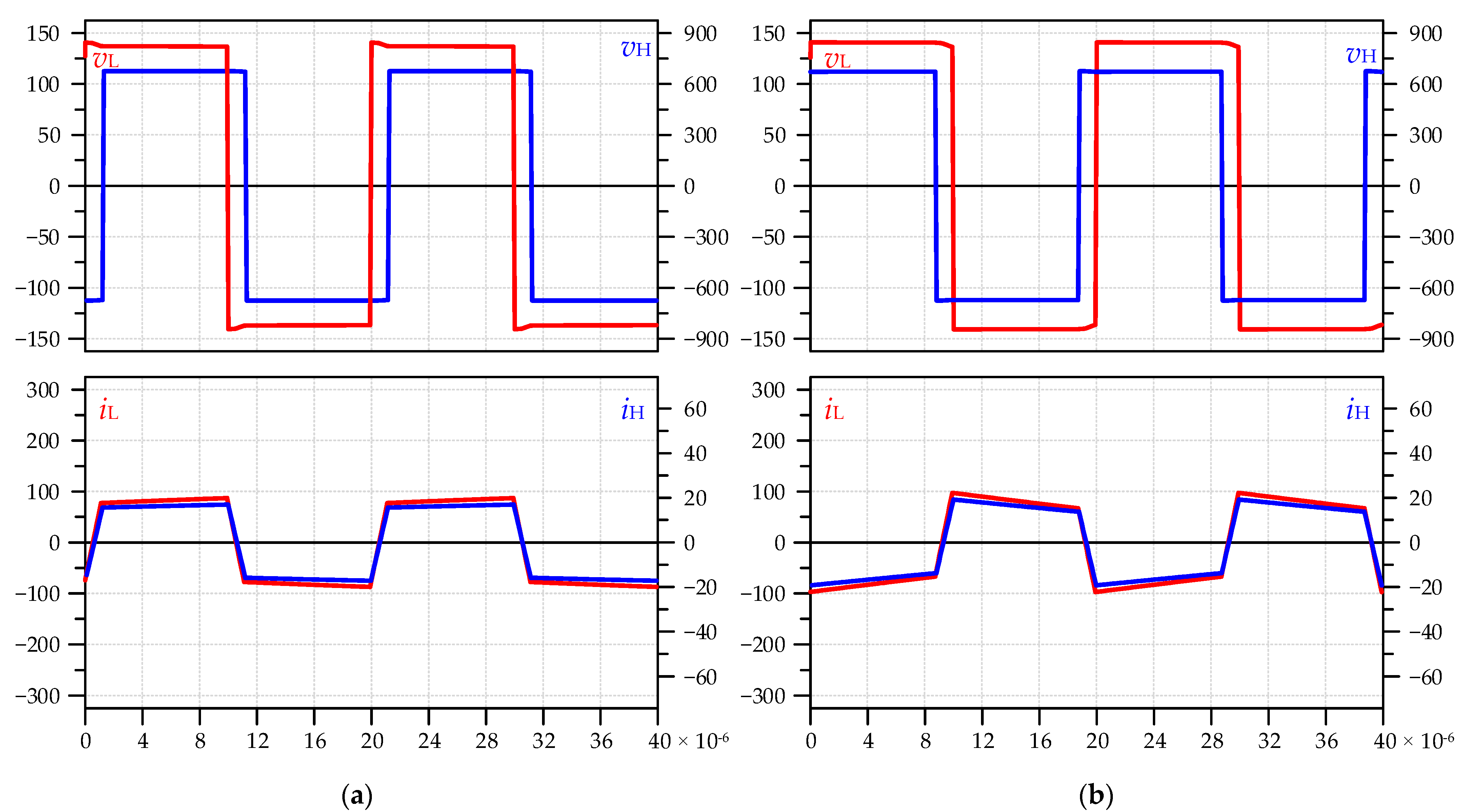
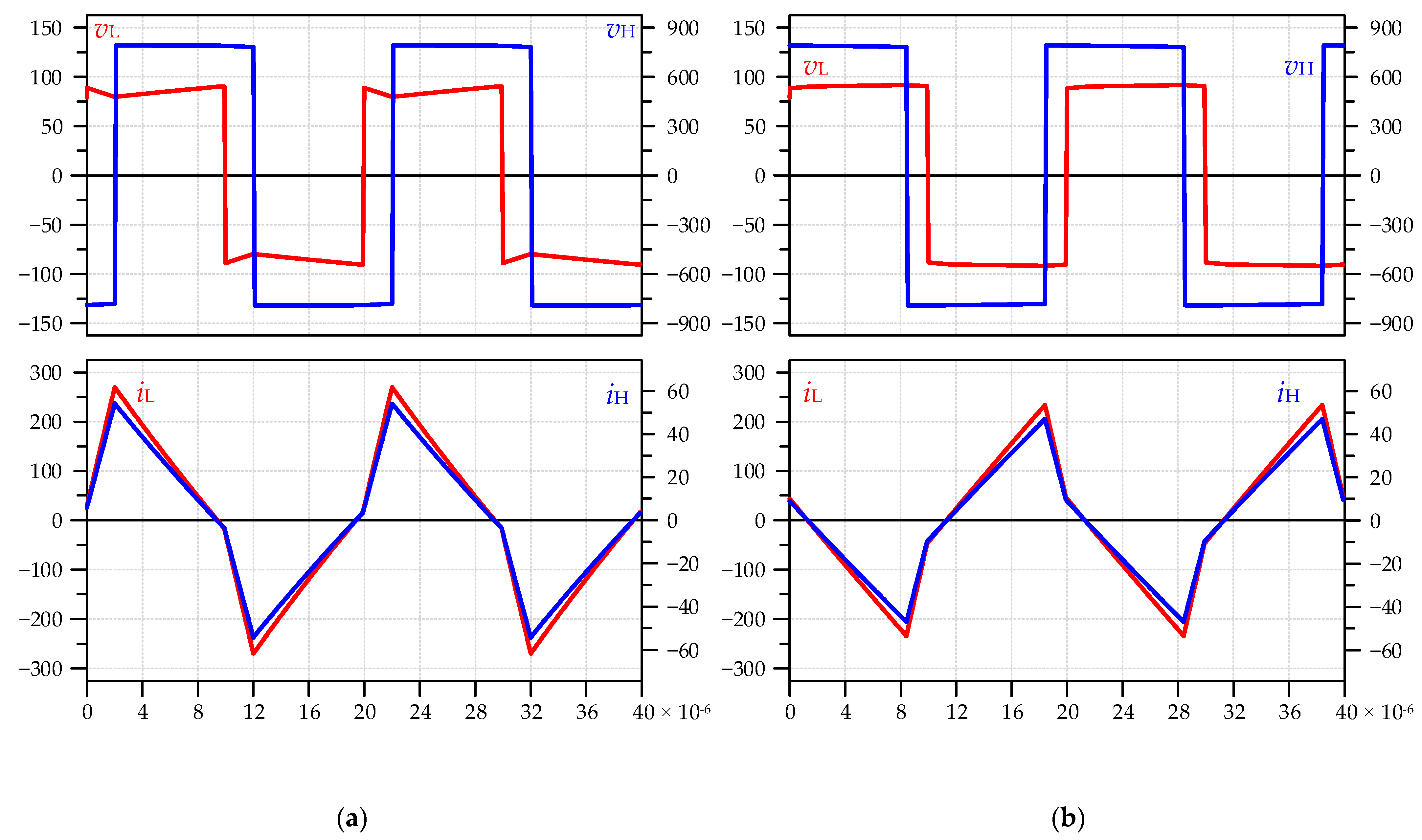
Example waveforms of voltages and currents of both H-bridge converters are depicted in
Figure 4,
Figure 5 and
Figure 6. These results were obtained for operation with a power of 10 kW during charging (a) and discharging (b) the battery and under various voltage conditions. When the low-side (fuel cell) voltage
VL equals 140 V, and the high-side (battery) voltage
VH equals 675 V (
Figure 4), the voltage ratio
VH/
VL is close to 5, which is the value of the transformer turns ratio. In this case, the currents are trapezoidal, and their maximum values are relatively low. In the case of the voltage mismatch (
VL = 140 V,
VH = 560 V), the currents reach higher maximum values—
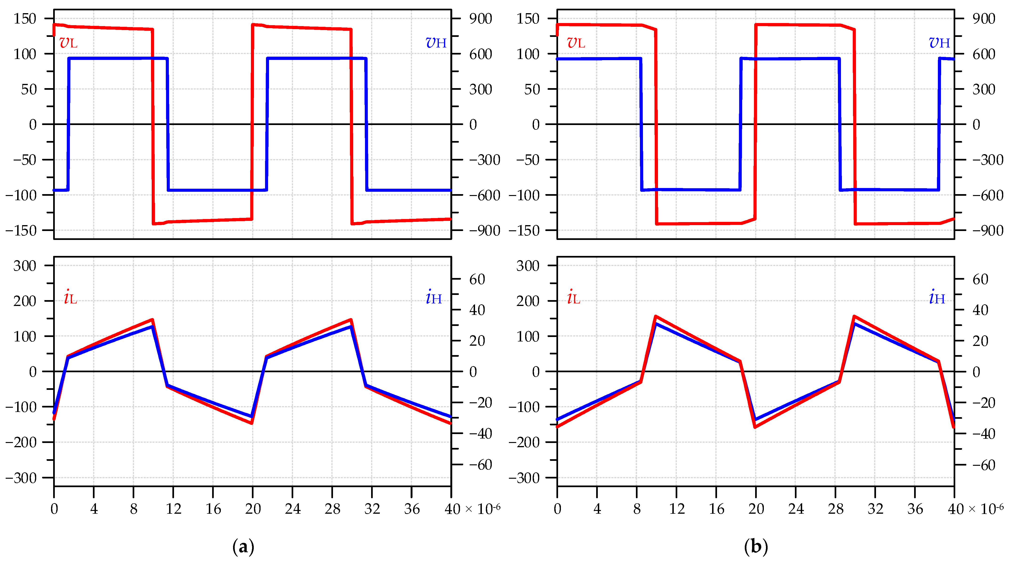
Figure 5. The results of the operation with the lowest voltage value at the fuel cell side (
VL = 90 V) and the highest voltage value of the battery (
VH = 790 V) are depicted in
Figure 6. In this case, due to the output-to-input voltage ratio being much different than the transformer turns ratio, the transformer currents are triangular and reach the maximum possible values (
Table 1). These values must be considered when designing the transformer, the inductor, and selecting the bridge transistors and dc-link capacitors.
Due to issues with designing a transformer with a power of 10 kW, it was decided to use two separate 5 kW transformers working in parallel. Each is supplied with a separate H-bridge converter and uses a separate inductor. This topology has been named the double low voltage stage (LVs) DAB converter. In the case of using two parallel circuits at the fuel cell side, the maximum current values of most components can be only half of the values of a single DAB converter with a single transformer. The exception is the battery side H-bridge, whose maximum currents remain the same as when using a single 10 kW transformer.
Table 1 shows that currents at the low-voltage side are five times higher than currents at the high-voltage side. The current at the low-voltage side reaching 274 A causes considerable conduction losses in all converter components.
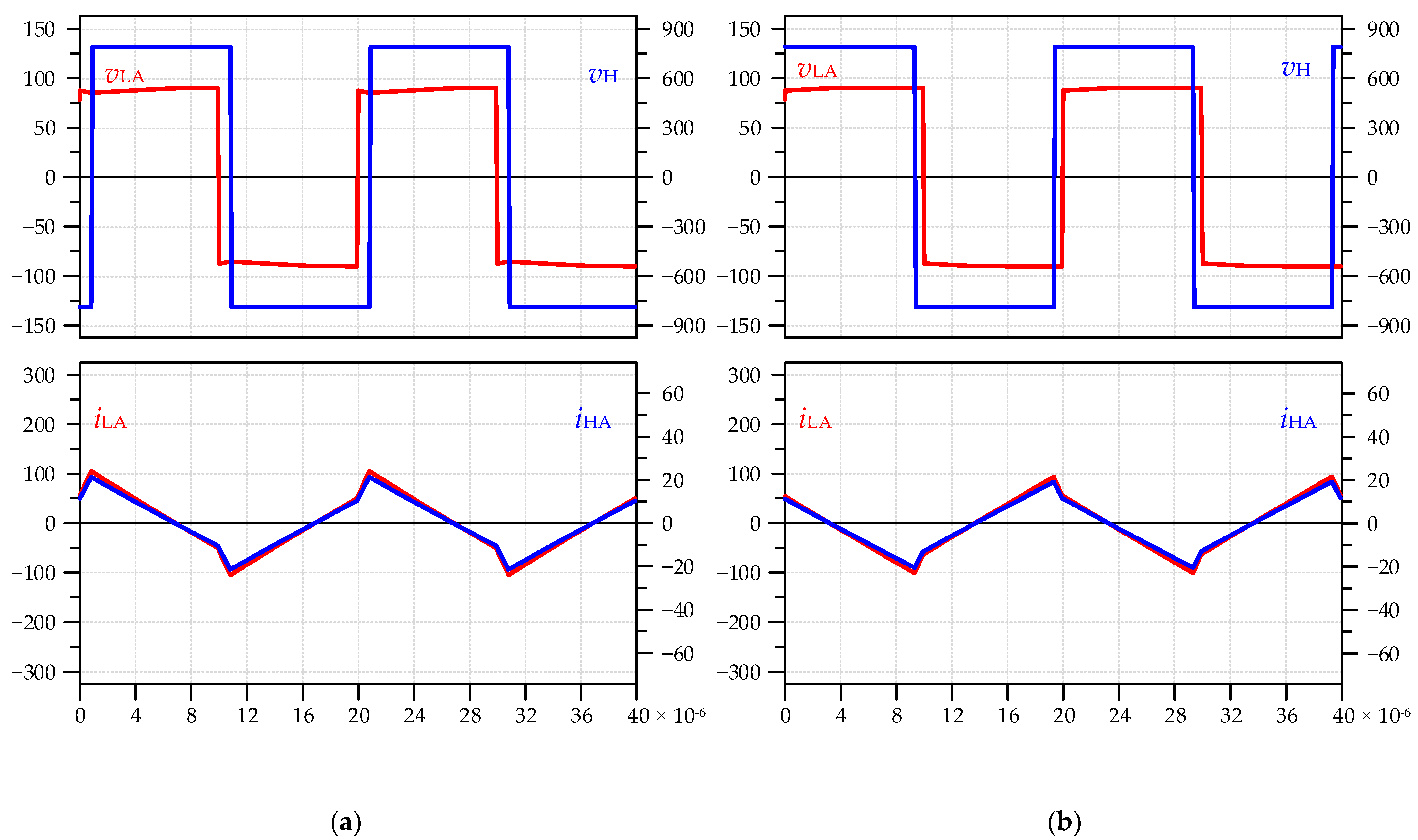
The final schematic of the designed double LVs DAB converter is depicted in
Figure 7, and input and output voltages and current waveforms are shown in
Figure 8.
The double LVs DAB converter ensures the reduction of currents in low-voltage side converter transistors and facilitates the construction of the DAB transformers using magnetic cores E71/33/32. The same cores have been used in the inductors. The double LVs DAB converter is additionally flexible and allows for changes, e.g., the number of operating transistors, switching off one of the low-voltage side converters, or easy disconnection of one transformer, which is analysed in Chapter 4. All topological modifications are intentionally applied to reduce converter power losses.
2.1. Magnetic Component Design
The selection of magnetic component parameters is based on the DAB converter’s operating parameters, particularly low-voltage side voltage
VL, high-voltage side voltage
VH, rated power
PN, and the switching frequency
fS.
VL and
VH voltages range from
VLmin to
VLmax and
VHmin to
VHmax, respectively. The values of all parameters used for designing transformers and inductors of both converters are listed in
Table 2.
The exact value of the transformer voltage and current can be obtained after selecting the inductor inductance
L and the transformer turns ratio
n. The selection procedure for the transformer parameters starts with the equation for the transferred power through the DAB converter (1).
where
D is a phase shift ranging from 0 to 0.5.
The transformer parameters are selected for known values of maximum currents and voltages in various operating conditions of the DAB converter. Because the best operating conditions in terms of the lowest power losses in a DAB converter occur under the assumption that the dc voltages are matched
nVL =
VH, and because it is expected that the converter will most often operate with rated voltages, it is assumed that the transformer turns ratio is given as follows (2):
The maximum inductance
Lmax (3) can be determined based on (1) with the assumption that the power is equal to its rated value
PDAB =
PN, the phase shift
D =
Dmax = 0.5, and that the voltages
VH and
VL are equal to
VLmin and
VHmin. If the inductance
Lmax is exceeded, for example, due to the presence of a higher leakage inductance of the transformer, this will limit achieving the maximum power.
In this paper, the inductor inductance is selected to be L = 75 μH with the assumption that the leakage inductance of the transformer increases the total inductance presented in (1) but is lower than the inductance given in (3). The reduced value of inductor inductance ensures the proper operation of the DAB converter with a margin for parasitic parameters’ influence and control during transients.
2.2. Transformer Design
The numbers of turns of transformer windings at the low-voltage side
N1 and high-voltage side
N2 are calculated together, considering the core size, material, and winding cross-sections. E-shaped cores made of 3C94 ferrite are chosen. Based on the product of winding window area
Aw and the cross-sectional area of magnetic core
Ac,
Ap =
AwAc (4), the appropriate core size is determined.
where
kCu is the winding filling factor
kCu = 0.3,
Bmax is the maximum flux density of the core
Bmax = 0.3 T,
Jmax is the maximum current density of windings
Jmax = 4 A/mm
2,
ILrmsmax and
IHrmsmax are the maximum rms values of currents at the transformer low-voltage side and high-voltage side, respectively, as in
Table 1. The values of currents are obtained from the simulation as
ILrmsmax = 83 A and
IHrmsmax = 16.6 A.
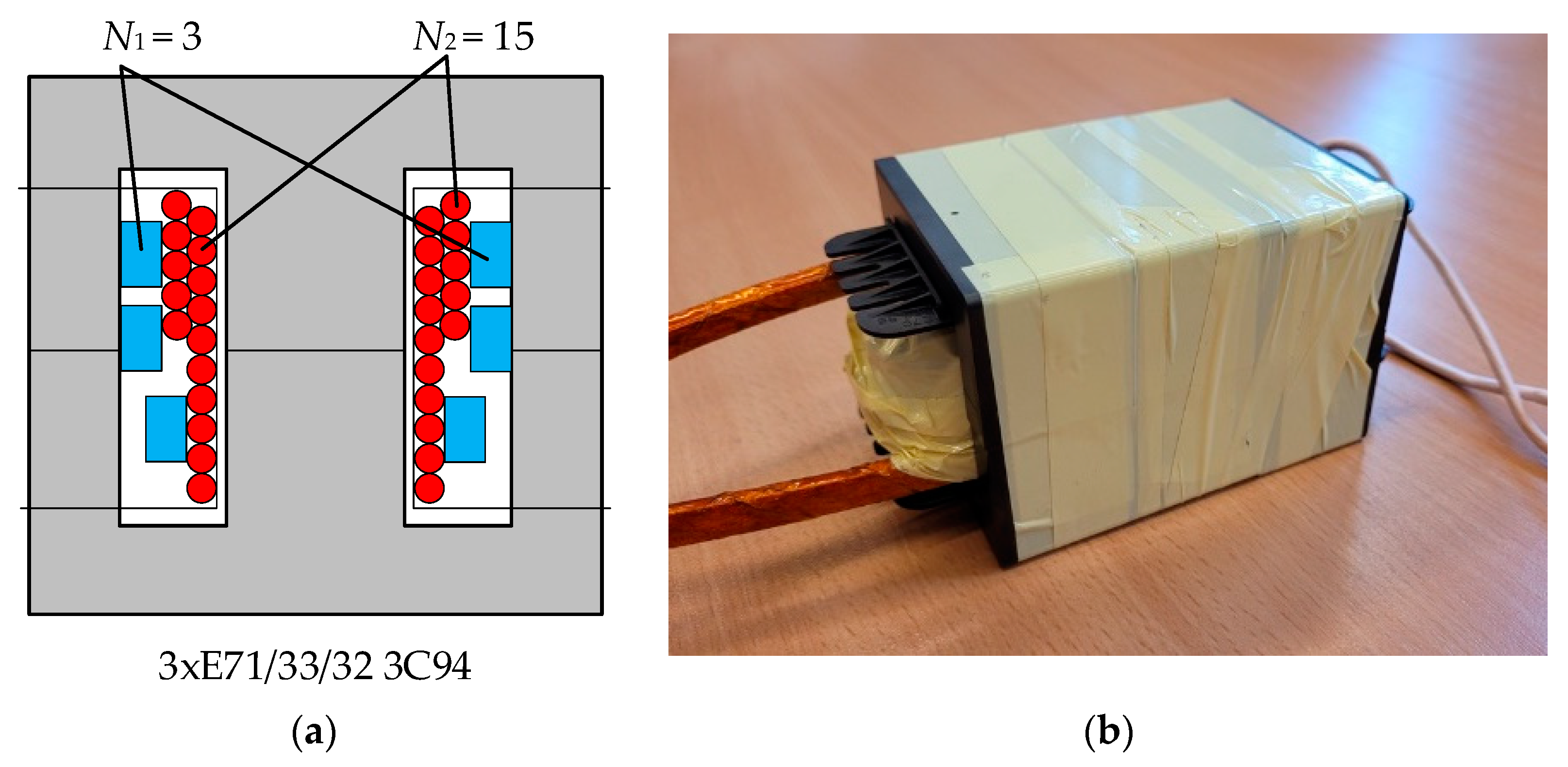
From (4), the product Ap = 802,333 mm4; therefore, the selected magnetic core has to have a higher value of Ap. The magnetic core, composed of 3 stacked cores E71/33/32, has been chosen for this paper. The total magnetic core area is Ac = 2049 mm2, the window winding area Aw = 569.4 mm2, and the resultant product Ap = 1,166,701 mm4.
The number of turns of the low-voltage side winding of the transformer
N1 is determined based on the condition for the value of magnetic flux density
B (5), which in the worst operating conditions, at
vL =
VLmax and for time
t =
TS/2, should not exceed the maximum value
Bmax = 0.3 T (6).
From (6), it is possible to derive the number of turns at the low-voltage side
N1 (7)
Assuming the number of turns
N1 = 3 means that the value of flux density in the transformer core in the steady state for time
t =
TS/2 will be approximately equal to ½
Bmax, which ensures the condition of non-saturation of the transformer core. The number of turns on the high-voltage side
N2 is determined based on the number of turns
N1 as in (8)
The selection of the cross-section of the transformer windings was made based on the simulation-determined maximum rms values of winding currents given (as in
Table 1) for power
PN = 5 kW, with the limitation that the current density does not exceed
Jmax = 4 A/mm
2, and for the switching frequency
fS = 50 kHz. Litz-type wires with a strand diameter of 0.1 mm are used for such a frequency. The winding cross-section areas
SCuL and
SCuH are determined in (9).
For the low-voltage side winding, a litz-wire of 2000 × 0.1 strands is selected with an equivalent cross-sectional area of 15.71 mm
2, and for the high-voltage side winding, a litz-wire of 630 × 0.1 strands is selected (with the equivalent cross-sectional area of 4.95 mm
2). The winding arrangement and photograph of the transformer are presented in
Figure 9. The selection of the litz-wire 2000 × 0.1 with a cross-sectional area of 15.71 mm
2 leads to an increase in the current density at the highest current to 5.3 A/mm
2, and is accepted by the authors.
2.3. Inductor Design
The inductor selection is based on selecting the magnetic core and the inductor winding. Due to the specific design of the DAB converter, the same magnetic core as for transformer E71/33/32 is selected for the inductor. The magnetic core has an air gap chosen with the number of turns NL to satisfy the value of inductance L = 75 μH and relatively high maximum current, which does not saturate the core.
Based on the product
Ap =
AwAc for designing the inductor, the selected magnetic core has to fulfil (10).
where
kCu = 0.2,
Bmax = 0.3 T,
Jmax = 4 A/mm
2,
IHmax and
IHrms are the maximum peak and rms values of the inductor current, and
kI is a safety margin which is
kI = 1.5. The values of currents are given in
Table 1.
The area product of a single E71/33/32 core is Ap1 = 388,900 mm4, and this value satisfies (10). Still, during the experimental tests of the converter, it was shown that the inductor core is overheated; thus, a set of two E71/33/32 cores is chosen as the inductor core. The number of turns and the air gap length are calculated to satisfy inductor inductance L = LA = LB = 75 μH and maximum current 27.5 A. The air gap length is selected to be lg = 1 mm, and the number of turns is NL = 8. With such parameters, the maximum current that does not saturate the magnetic core is above 55 A.
2.4. Bridge Design
The voltage ratings of transistors and dc-link capacitors on both sides result from the voltage ranges of the lower and upper voltage sides assumed in the design. The results of preliminary simulation tests made it possible to determine current requirements. In the case of a low-voltage bridge, transistors with a drain-source voltage of at least 250 V are required. It is safe to assume 150 A as the maximum transistor current. In this voltage range, the best-suited transistor technology seems to be the silicon MOSFET. However, this is not so obvious considering the dynamic parameters and losses of SiC MOSFETs. In particular, the low value of the reverse charge
Qrr of the body diode makes these transistors recommended for hard-switching converters. This means that SiC technology should also be considered in the converter design on the low voltage side, even though the lowest available voltage class is 650 V.
Table 3 shows the parameters of several selected transistors. Since the parameters characterising switching losses are presented in the datasheet for the rated voltage, their use at lower voltage leads to even lower switching losses.
With the assumed rated currents, the first choice for the transistor package should be a module type. Among SiC transistors, module packages are only available for the higher voltage ratings. Therefore, a design based on discrete transistors is chosen. Thanks to package standardisation, the risk of the availability of a specific model on the market can be reduced. On-state resistances of several dozen milliohms directly affect conduction losses. For example, for 20 mΩ and a current of 60 A (which is still a permissible value), the power dissipated in a single transistor would be 72 W. Such a value is unacceptable; therefore, connecting several transistors in parallel is necessary. At the same time, increased switching losses must be taken into account.
To limit the inductance of the gate circuit, only packages containing an additional terminal at the source, serving as a reference point in the gate circuit, have been considered. This decreases the inductance inside the gate circuit and thus reduces switching losses. It also reduces the susceptibility to accidental switching caused by voltage induced by a rapid change of the source current. Therefore, the TO-247 package has been declined (also due to the small cross-section of the drain and source pins). In turn, systems in screw-mount packages like SOT227B are characterised by a relatively high diode reverse charge. At the frequency of
fS = 50 kHz, this may lead to high overvoltages. In that case, the focus has been on devices in TO263-7L packages. A large equivalent cross-section for drain and source terminals in a transistor with five parallel source legs ensures low resistance and inductance. At the same time, the expected current density is significantly lower than in the TO247-4 package. Finally, the IMBG65R022M1HXTMA1 from Infineon, recommended by the manufacturer for hard-switching topologies, has been selected as the low-voltage H-bridge converter transistor [
27]. Four transistors, which are connected in parallel, are used as a single transistor.
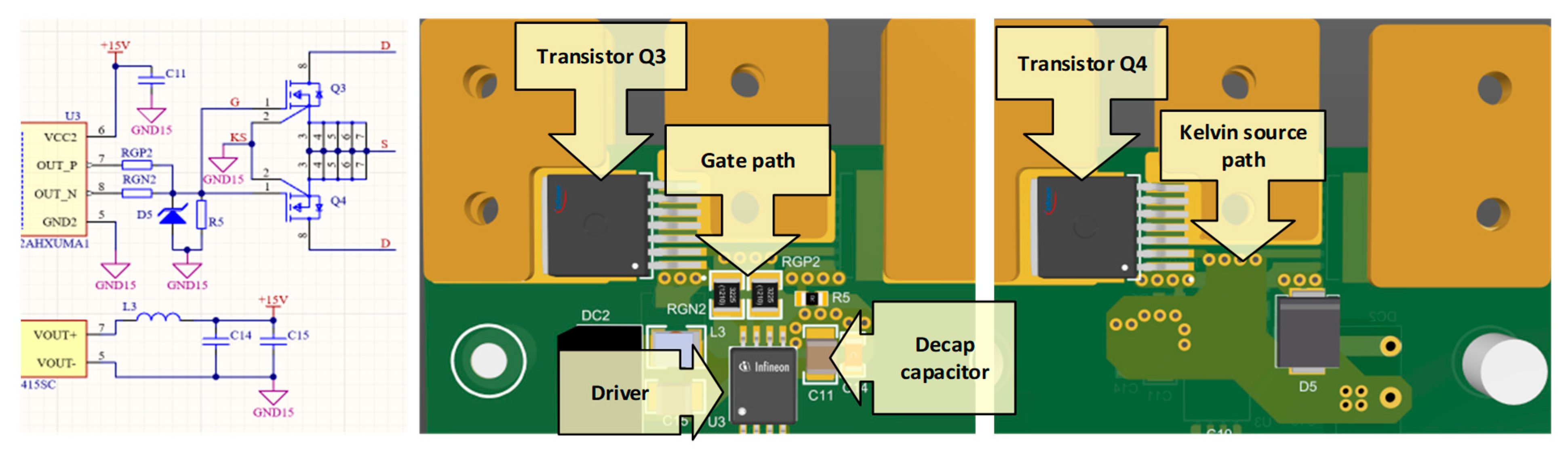
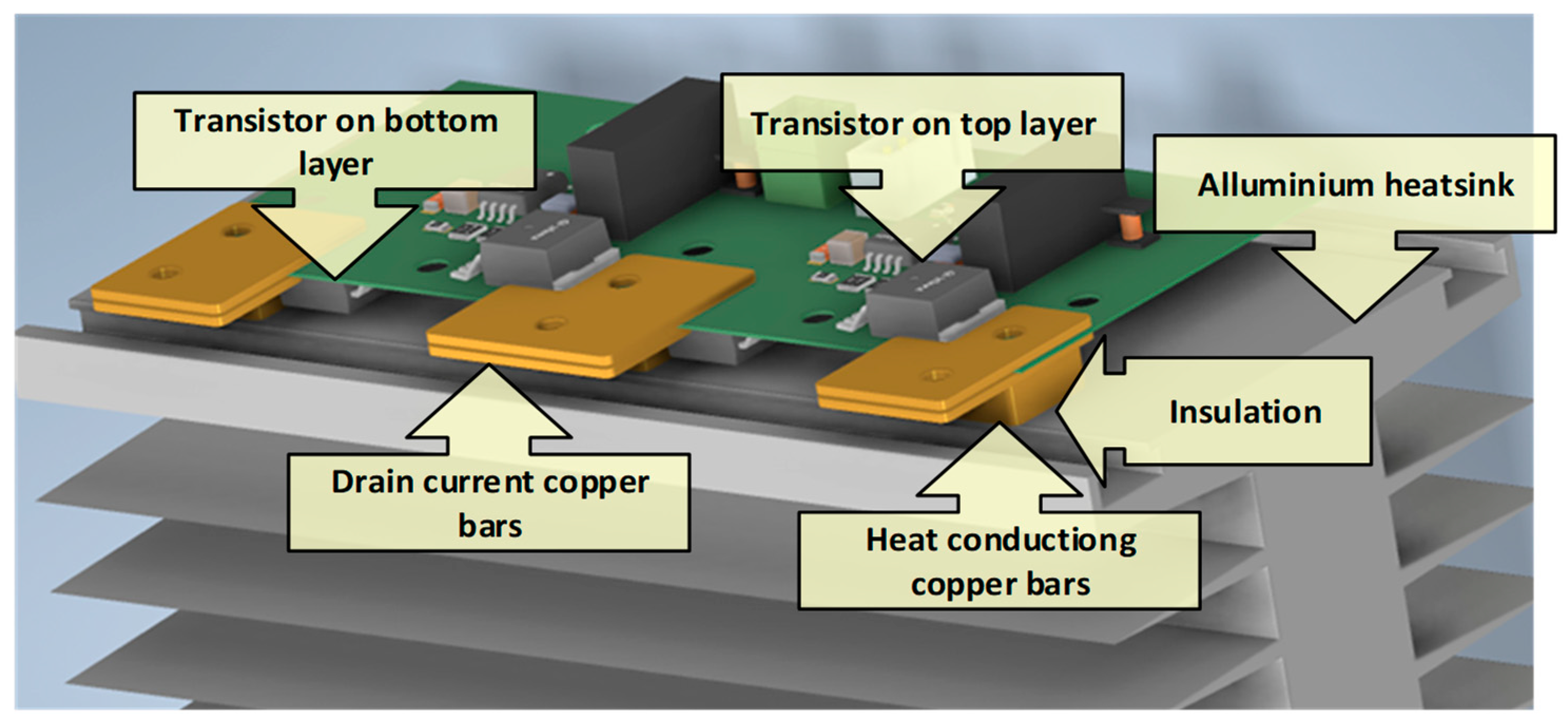
Two drivers 1EDC60H12AH, each providing a maximum 6 A gate current, are selected to drive these transistors. The driver circuit is designed with a focus on the minimisation of connection length for reducing parasitic inductance. In the case of TO263-7L packages, the maximum proximity of the transistors to the driver while providing enough space for the high-current circuit is achieved by placing two transistors on opposite layers of the printed circuit board. The symmetry of the gate circuit can then be performed, ensuring synchronous switching of both transistors. The arrangement of the devices on the PCB is shown in
Figure 10. The gate circuit consists of separate resistors for turning the transistor on and off (RGP2 and RGN2), a Miller clamp diode (D5), and a pull-down resistor (R5). The paths supplying current to the gate are mainly on the top layer. The return path from the Kelvin source terminals is routed by a wide track on the bottom layer, directly under the gate circuit, which minimises the stray inductance. The energy source for switching the transistors is a decoupling capacitor placed close to the driver.
The TO263-7L package is selected as appropriate for currents up to 150 A. The more considerable distance between the source and drain than in the TO247-4 package makes it easier to provide each terminal with a wide path with low resistance and inductance. The printed drain and source circuit paths were prepared without solder masks to be reinforced with additional 1 mm thick copper plates. The only construction issue of the TO263-7L package is the dissipation of heat. This package transfers losses through the drain, and a properly designed printed circuit board should transfer the heat from the transistor and isolate the drain from the heat sink [
28].
Figure 11 shows a 3D model of the designed path dissipating heat to the heat sink where 1 mm copper plates connect the transistor drain to the dc-link. An additional 5 mm copper plate transports heat from the PCB circuit to the heatsink. A suitable thermal pad was used between the copper bar and the heatsink, ensuring isolation from the drain.
In the design of a dc-link circuit, it is necessary to ensure an acceptable level of voltage ripples at the expected dc-link ac current [
29]. Using SiC MOSFET transistors requires careful design of the connection between capacitors and transistors [
30]. The operation of the converter with voltage mismatch on both sides of the converter is associated with the occurrence of non-trapezoidal currents (
Figure 5 and
Figure 6). In this case, the rms value of the ac component of the dc-link at the low-voltage side reaches 42 A. For this reason, the construction of the dc-link with only polypropylene capacitors has been chosen.
Table 4 contains the parameters of selected capacitors considered for the dc-link circuit. An electrolytic capacitor is shown in the first column only for comparison with the polypropylene capacitors.
Among polypropylene capacitors, components with four terminals and low equivalent series resistance are noteworthy. The smaller dc-link circuit dimensions can be obtained using components with a small pin spacing. Therefore, capacitors with larger capacitance were declined due to their larger sizes and proportionally lower current ripple. Finally, the C4AQCBW5500A3OJ capacitor from KEMET was selected for a dc-link using seven parallel capacitors [
31]. This number ensures an acceptable voltage ripple level, and the dimensions of the DC circuit match the dimensions of the H-bridge PCB. The capacitors have been mounted on the PCB, and the traces have been prepared to increase the cross-sectional area with additional copper bars.
Figure 12 shows the 3D model of one of the low-voltage H-bridge converters. The high-voltage bridge has a similar structure. The PCB circuits corresponding to transistors are placed on separate heat sinks. A capacitor PCB is connected to transistor terminals between the created transistor modules of the positive and negative groups. In this way, the distances between transistors and capacitors are minimised. The entire circuit is completed by connecting the sources of the upper transistors and the drains of the lower transistors of each half-bridge. This is accomplished by using a large copper plate placed above the capacitors. In this way, it is also possible to minimise the equivalent inductance of the circuit. Since these plates are the midpoints of the half-bridges, they are also convenient places to connect the wire leads of a transformer or inductor.
3. Experimental Tests of the DAB Converter
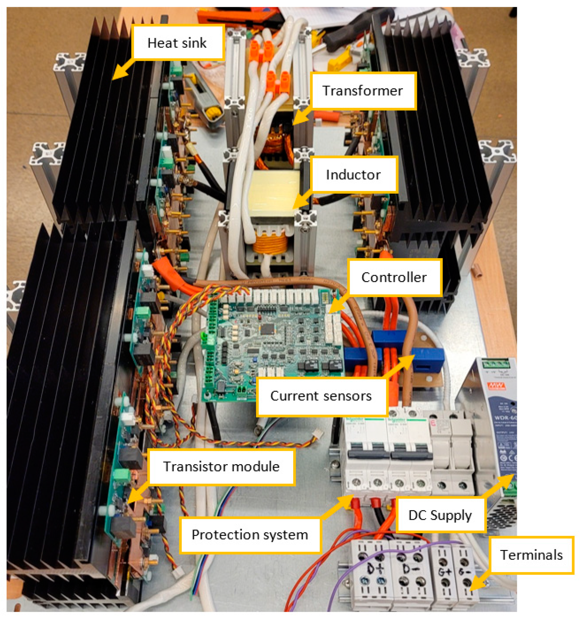
A photo of the designed DAB converter is shown in
Figure 13. As mentioned above, the converter consists of:
Two low-voltage side H-bridge converters (top left and right),
Two transformers and inductors (top centre),
One high-voltage side H-bridge converter (bottom left)
Microprocessor-based controller (centre),
Current sensors, protection system, and 24 V DC power supply (bottom right).
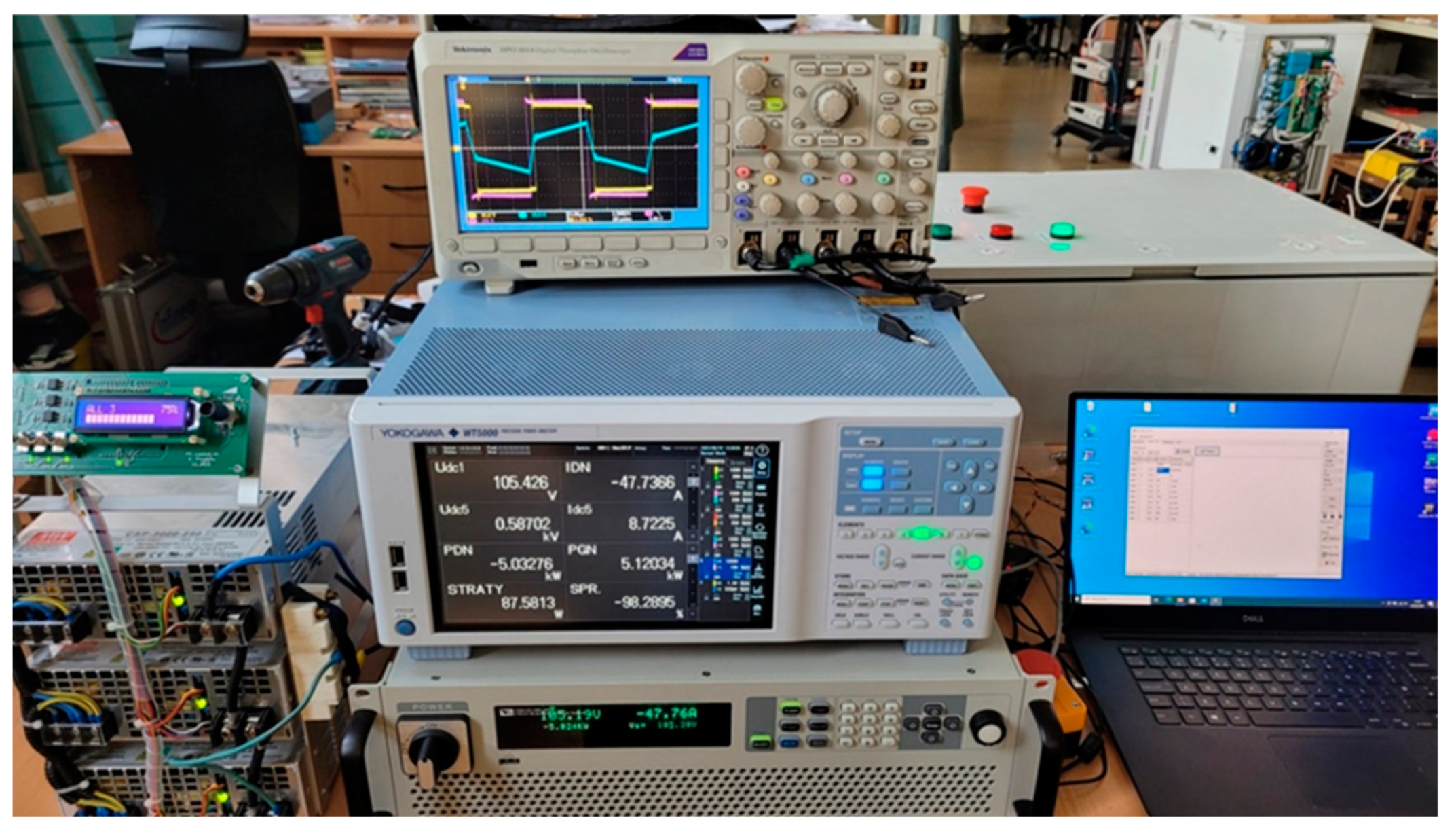
The DAB converter was placed into a housing and experimentally tested (
Figure 14). Two laboratory DC power supplies were used as battery and fuel cell models during the tests. A Yokogawa WT5000 power analyser was used to measure input and output voltages, currents, and powers. A PC was used for communication with the DAB controller via the RS-485 bus and MODBUS protocol. The experimental tests included efficiency and waveform measurements.
The DAB converter was tested under various voltage conditions. The microprocessor-based controller stabilised the power on the low-voltage (fuel cell) side. Tests were carried out for power varying from 1 kW to a value depending on the maximum current of the DC power supply used instead of the battery.
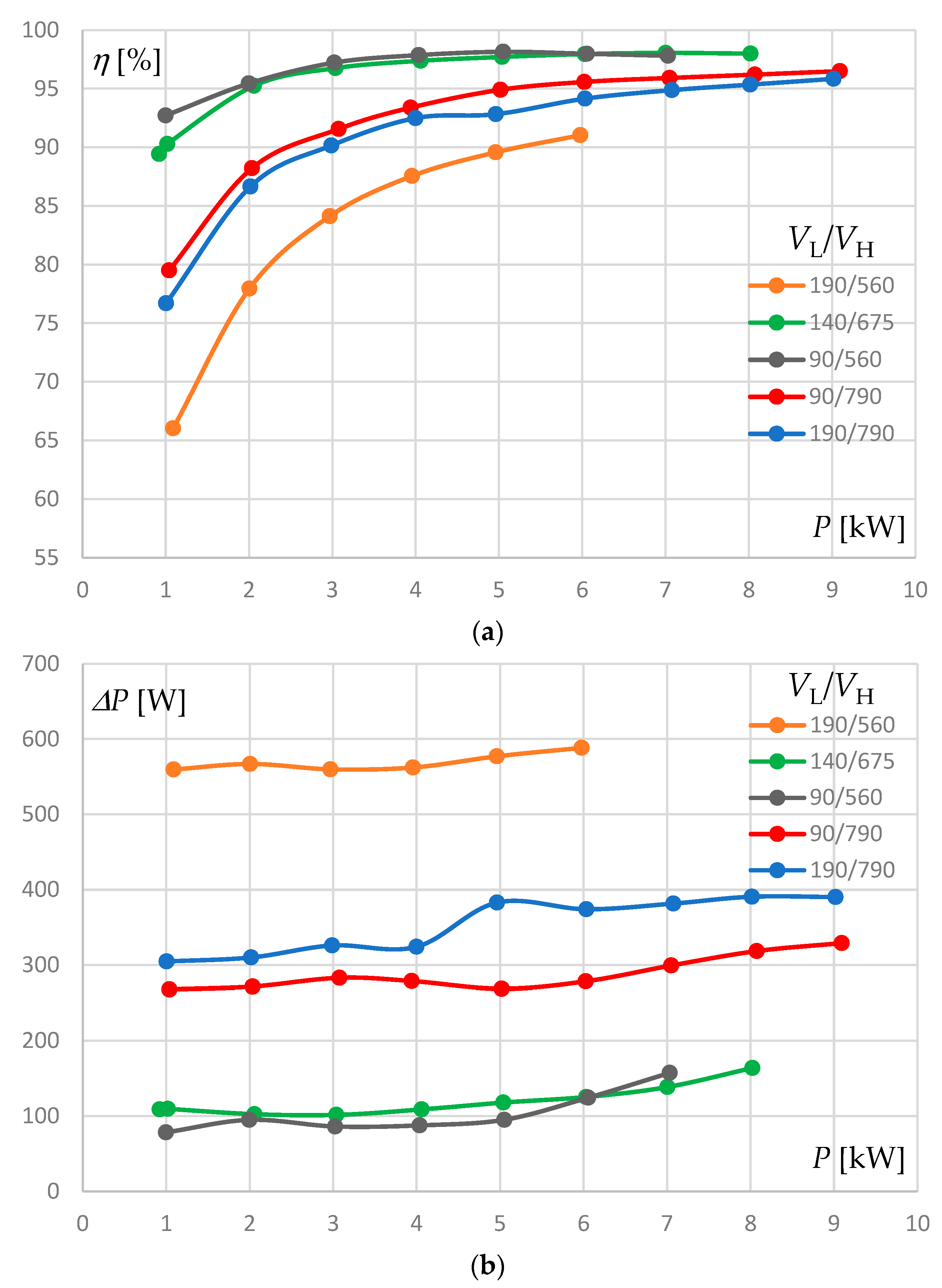
The efficiency and power loss characteristics of the DAB converter are depicted in
Figure 15. As expected, the best efficiency is achieved when the voltage ratio is close to the turns ratio of the transformer (green line), i.e.,
VL = 140 V and
VH = 675 V. This is because both low-voltage and high-voltage side converters operate with ZVS conditions [
8]. Similar relatively small power losses are obtained for
VL = 90 V and
VH = 560 V (grey line). For such voltages, the ratio
VH/(
nVL) = 1.244 and the ZVS condition is met at the low-side converters when the phase-shift is
D = 0.098, corresponding to the power transfer of 4400 W [
8]. It should be noted that these conditions are characterised by the lowest voltages,
VL and
VH, and switching losses in non-ZVS conditions are the lowest compared to other situations.
A voltage mismatch (red and blue lines in
Figure 15) leads to a reduction in efficiency. For example, when
VL = 90 V and
VH = 790 V (red line), the ratio
VH/(
nVL) = 1.756, and both low-voltage side converters experience non-ZVS conditions across the whole range of transferred power. The opposite situation occurs when
VL = 190 V and
VH = 790 V (blue line), and the ratio
VH/(
nVL) = 0.832. This causes the high-voltage side converter to operate without the ZVS condition. However, the worst conditions occur when
VL = 190 V and
VH = 560 V (orange line). Operating with the ratio
VH/(
nVL) = 0.589 causes the high-voltage side converter to experience hard-switching at relatively high currents, leading to increased power losses. Additionally, with increased
VL voltage, power losses in the transformer core increase.
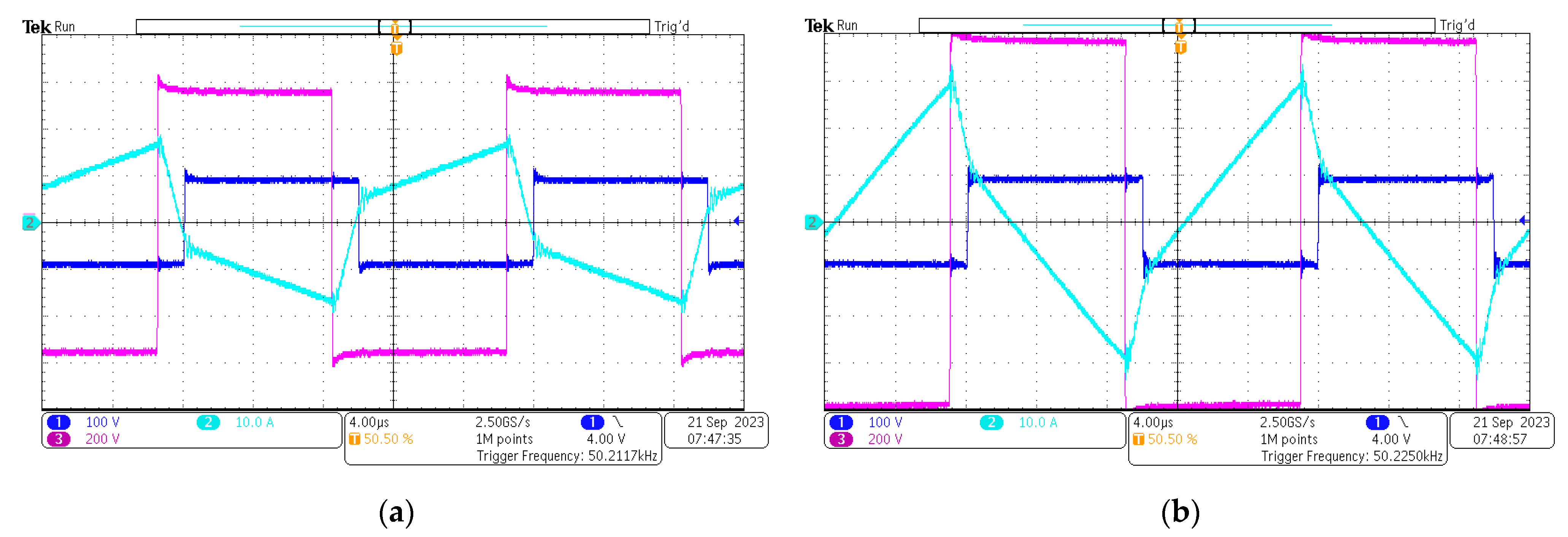
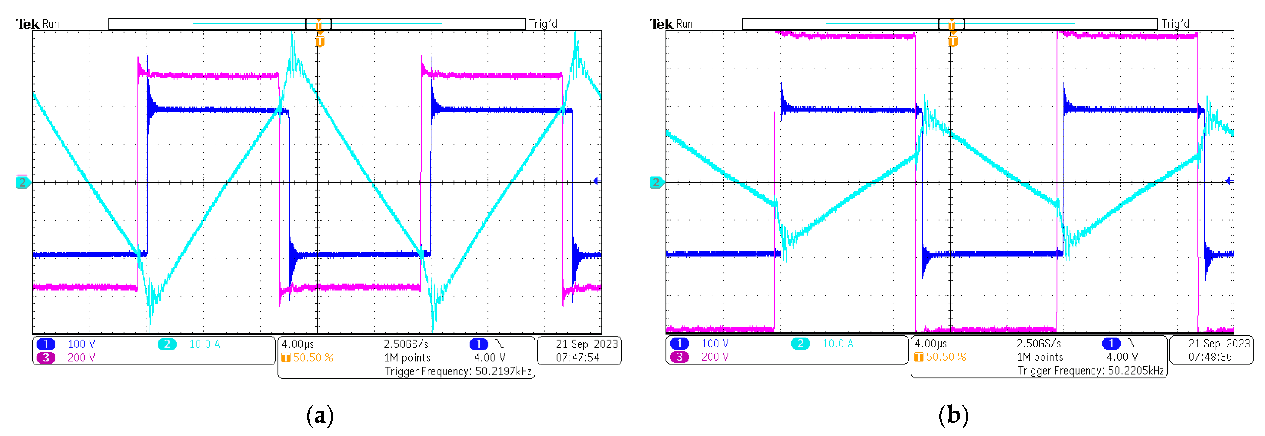
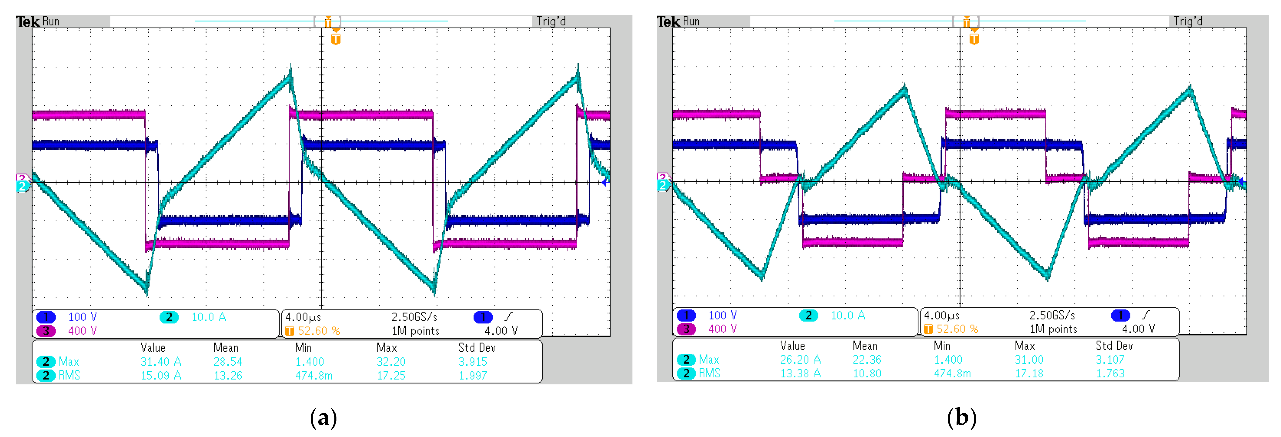
Waveforms of the fuel cell side H-bridge voltage (dark blue), battery side H-bridge voltage (magenta), and battery side H-bridge current (cyan) are depicted in
Figure 16 and
Figure 17. These waveforms are taken under the same voltage conditions as the efficiency measurements during battery discharge with a power of 6 kW. Bidirectional operation of the converter is depicted in
Figure 18. In this case, the converter operates with
VL = 140 V and
VH = 700 V.
The operation with ZVS conditions in converters on both sides is presented in
Figure 16a and
Figure 18. In
Figure 16b, the low-voltage side converters switch on with non-ZVS conditions. The opposite situation occurs in
Figure 17, where the high-voltage side converter switches with non-ZVS conditions in both examples.
4. Discussion on Efficiency Improvement
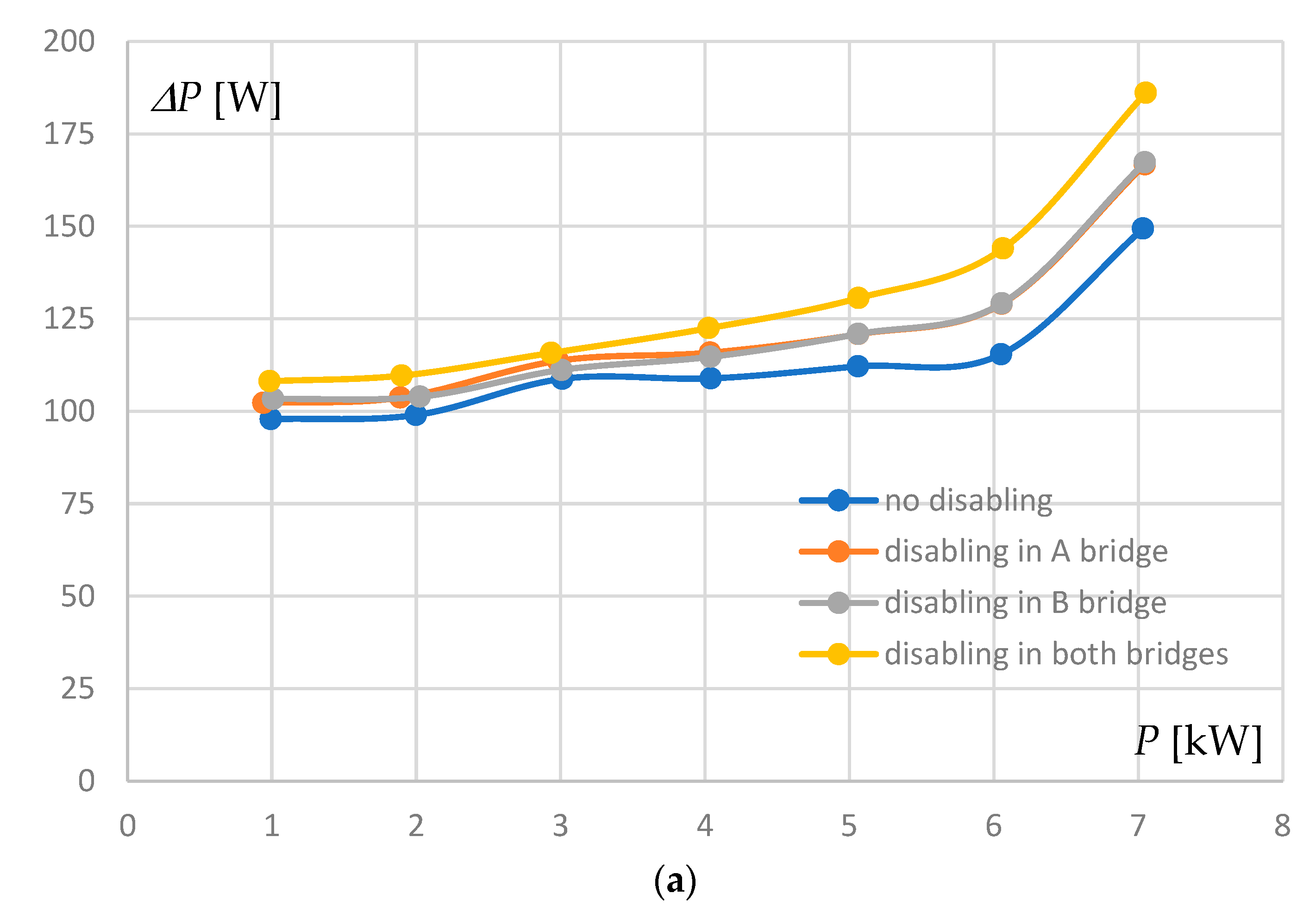
As mentioned in
Section 2.4, each transistor module of both low-voltage side H-bridge has four component transistors connected in parallel. The microprocessor controller provides a digital signal, which allows for the turning-off of two component transistors in each transistor module. This can be done for both fuel cell side H-bridges separately. Turning off the component transistors can be beneficial when the DAB converter works at low power and should reduce switching power losses. In the project, the power below which the modification is applied is equal to 50% of the rated power.
The characteristics of power losses of the DAB converter operated under the following conditions:
VL = 96 V,
VH = 610 V, are shown in
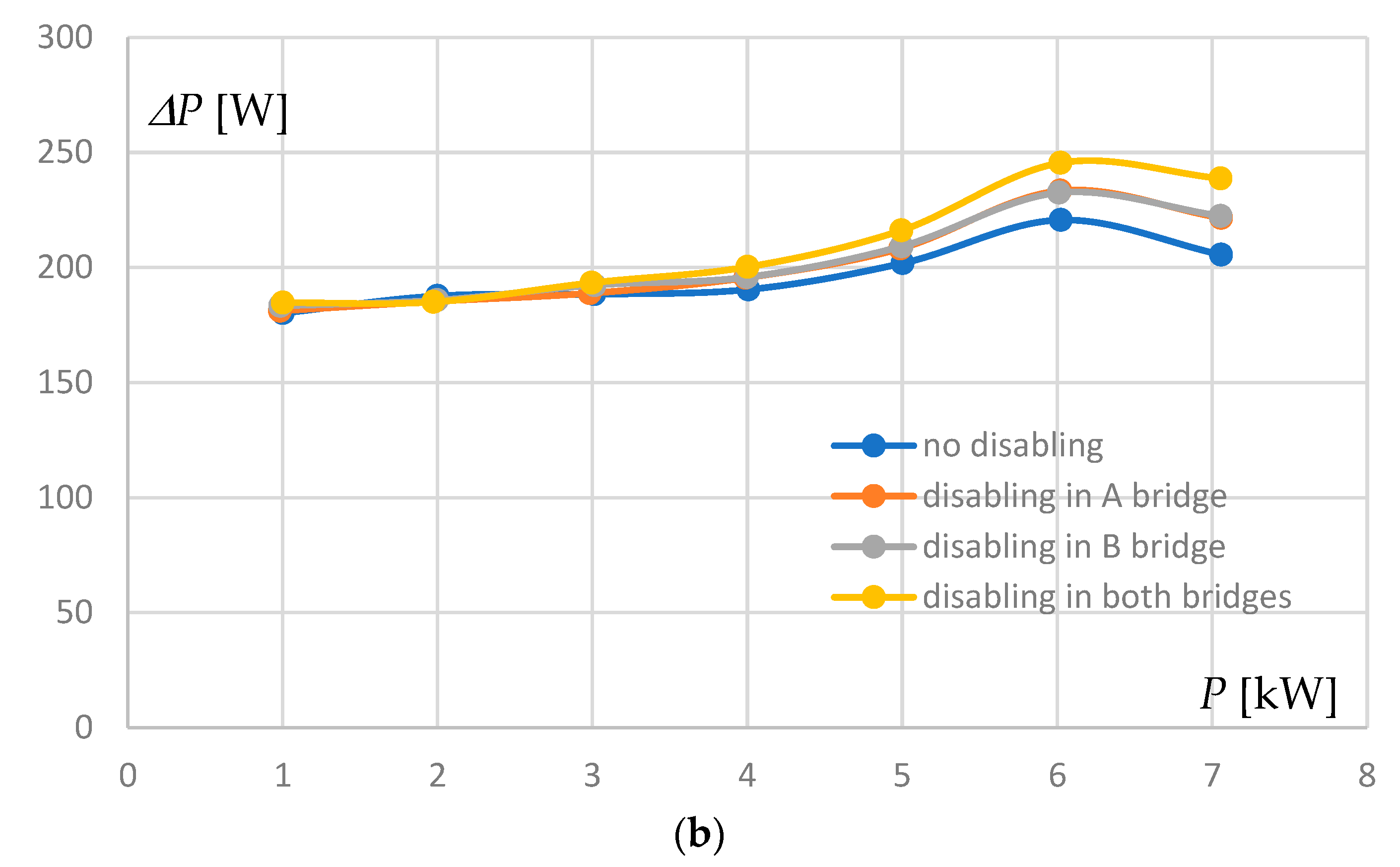
Figure 19a. When all transistors are used, power losses reach the lowest level (blue line). In the case of operation with a reduced number of parallel transistors in one of the low-voltage side H-bridges (referred to as “A”), power losses reach a higher level (grey line).
The same results are obtained when the second low-voltage side converter (referred to as “B”) operates with half of the component transistors (orange line). The highest power losses occur when disabling signals are applied to both fuel cell side H-bridge converters (yellow line). Similar results are obtained for voltages
VL = 156 V and
VH = 680 V (
Figure 19b).
This leads to the conclusion that conduction power losses in the H-bridge transistors are dominant compared to switching power losses. With a reduction in the number of switched-on transistors, the equivalent turn-on resistance is increased, leading to an increase in conduction power losses. The increase in conduction power losses is higher than the decrease in switching power losses due to the reduced number of switching transistors.
As shown in
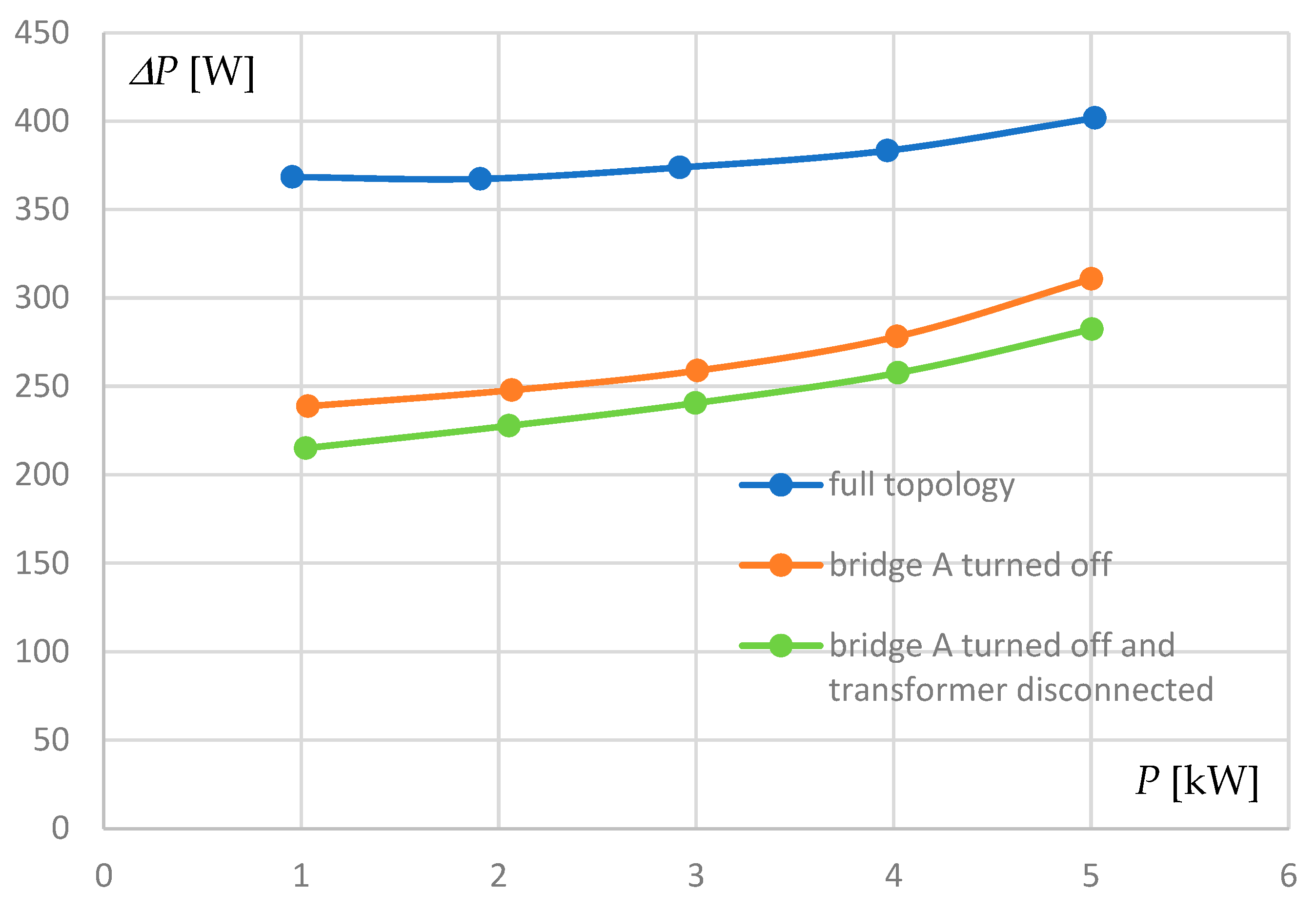
Figure 19, turning off the redundant transistors does not significantly reduce the power losses in the DAB converter. Another idea to increase the efficiency is to change the topology of the converter. An example characteristic of power losses for
VL = 170 V and
VH = 560 V is depicted in
Figure 20. The first step is to turn off one low-voltage side H-bridge while leaving the transformer connected (orange line). The second step is to disconnect the transformer (green line). Resultant power losses are lower in both cases than in the original topology (
Figure 7). Reducing power losses using the disconnection of part of the converter is practical up to half of the rated power. The above tests were carried out for different
VL and
VH values, and the results are similar—in each case, the lowest level of power losses is obtained when working with only one transformer.
Figure 20 also shows the reduction in power losses resulting from disconnecting the transformer from the non-operating H-bridge converter A. It should be mentioned here that when the A converter is turned off, its transformer currents also do not flow, and the observed reduction in power losses (between 20 and 30 W) results mainly from reducing transformer core losses.
Another method to increase the efficiency is to change the control strategy. All previous results are obtained for the SPS method, where voltage
vL and
vH are rectangular (
Figure 3), and power control is based on phase shift changes. Another control method that gives preliminary promising results is proposed as a different solution. The authors of the paper name the method an Extended Phase Shift matched (EPSm). In the EPSm method, besides the phase shift between H-bridges, the additional reduction of the internal duty cycles of low-voltage and high-voltage side converters
DL or
DH is used. These duty cycles depend on the
VH/
VL ratio as in (11).
The idea of this method is similar to other control methods like EPS, DPS, or TPS. In contrast to them, where DH and DL computations are complex, in the EPSm, the duty cycles DH and DL are computed to match the voltages n vL to vH. It operates with the duty cycle calculated separately in each of the H-bridge converters as in (11).
The effectiveness of the EPSm method is compared to the SPS method using a simulation model. The results are presented in
Figure 21 and
Figure 22, including gate control signals of the upper transistor in each half-bridge, H-bridge voltages, and one of the inductor currents.
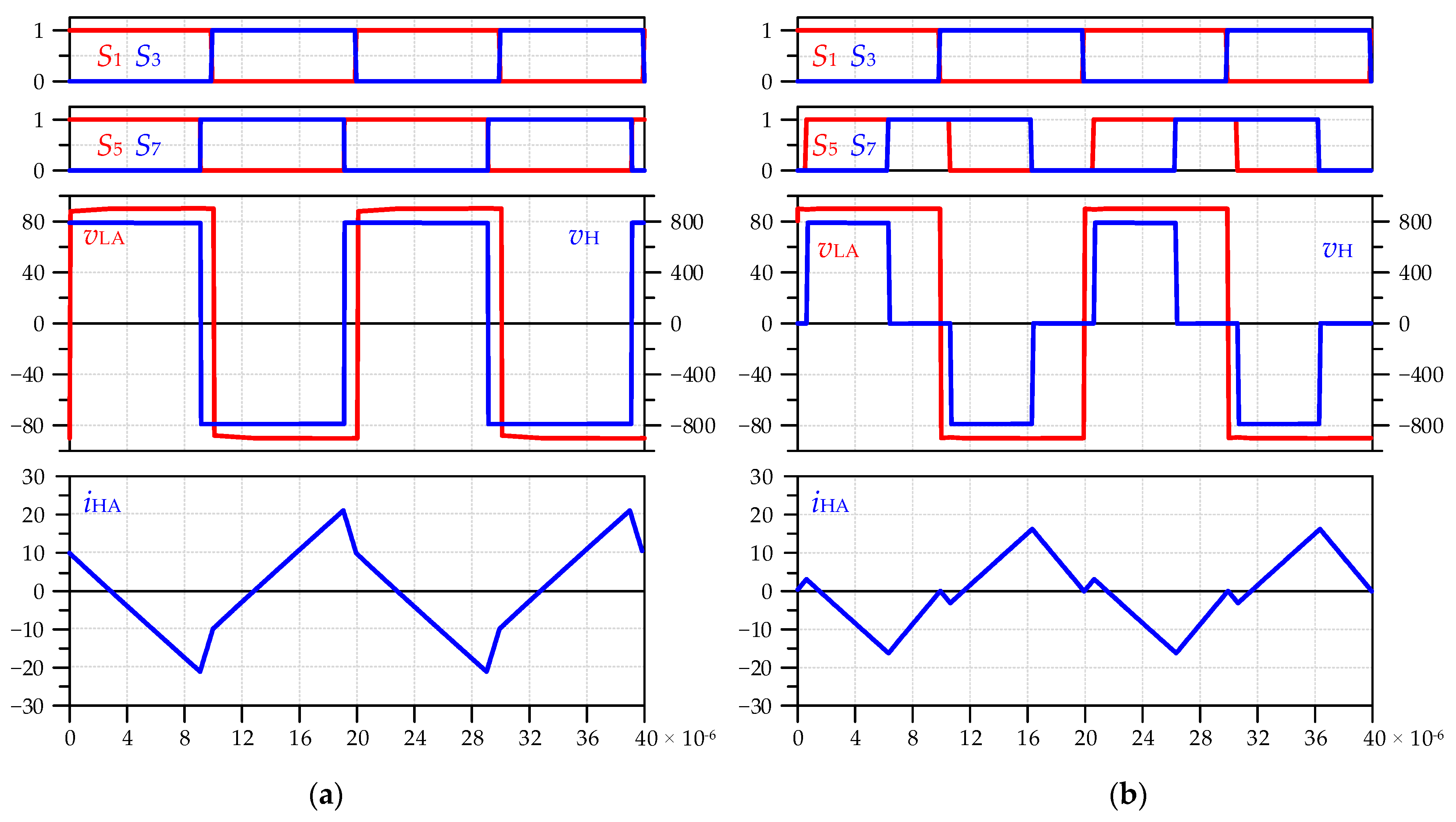
Figure 21 presents waveforms during the operation with
VL = 90 V and
VH = 790 V, and battery discharging at a power of 6 kW. One can see that the EPSm method reduces inductor circulating current by means of the reduction of the
DH duty cycle and fitting the values 0.5·
nVL and
DH·
VH. It can also be seen that the fuel cell side bridge transistors are switched at a current close to zero.
In
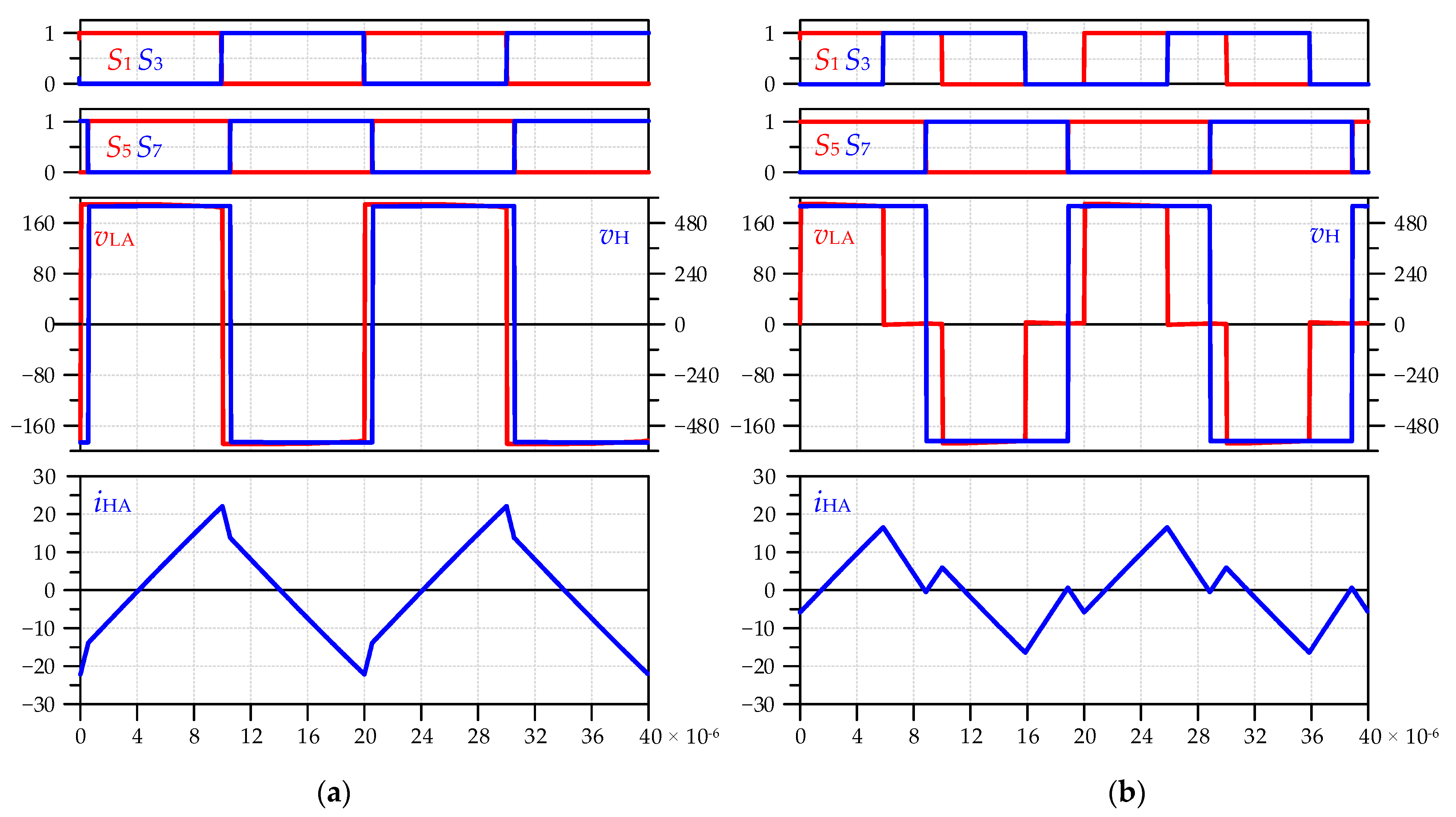
Figure 22, the operation with
VL = 190 V and
VH = 560 V for battery charging with a power of 6 kW is presented. Once again, the inductor current is reduced using the EPSm method, but for such conditions, the duty cycle
DL is reduced to fulfil the need of fitting the values
DL·
nVL and 0.5·
VH. For the situation presented in
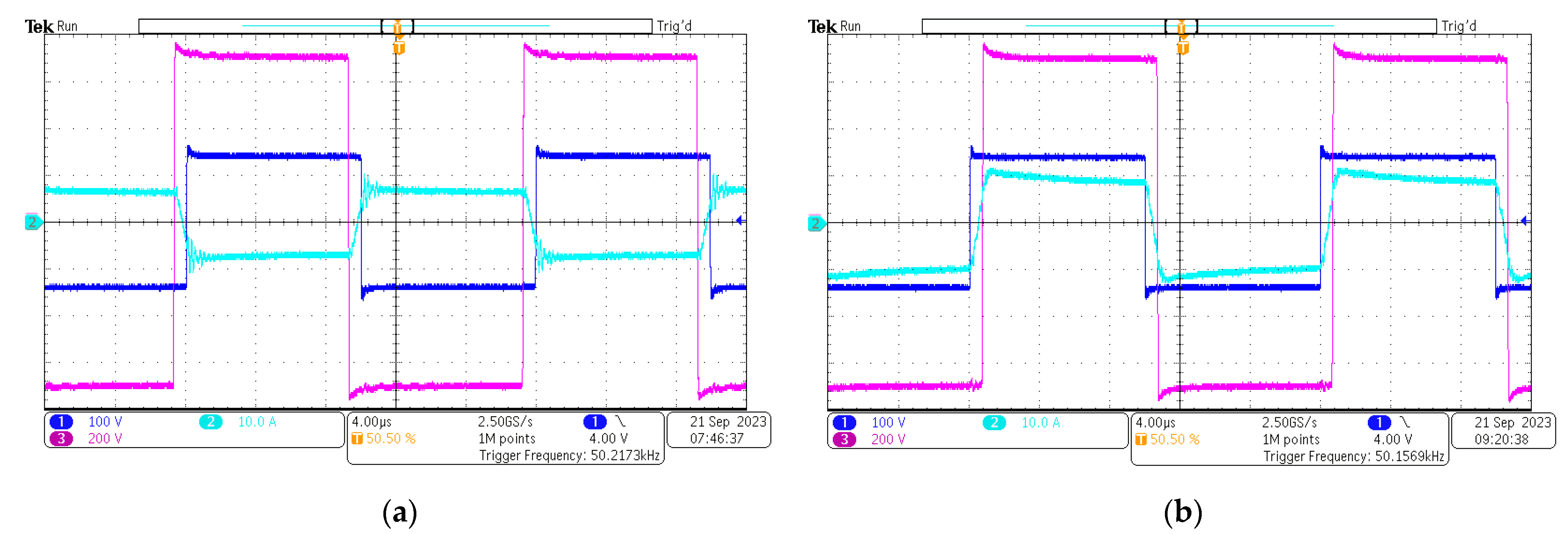
Figure 22, the battery side bridge transistors are switched with the current being close to zero.
Waveforms of the fuel cell side H-bridge converter voltage (dark blue), battery side H-bridge converter voltage (magenta), and the battery side H-bridge current (cyan) are shown in
Figure 23. These waveforms were taken in the laboratory under the following conditions:
VL = 96 V,
VH = 680 V, and
P = 6 kW. As can be seen, the maximum current for the SPS method (
Figure 23a) reaches a higher value than for the EPSm method (
Figure 23b). A comparison of power losses for both control methods, measured under the same voltage conditions, is depicted in
Figure 24. The EPSm method can reduce power losses by up to 50%. Experiment results with the implementation of the EPSm method are interesting, and the authors plan to conduct a thorough analysis in future investigations.
5. Conclusions and Future Research
A 10 kW DAB converter, operating as an interface between the LiFePo4 battery and the fuel cell/hydrogen generator, was designed, built, and tested. This converter enables bidirectional operation in a wide input and output voltage range. Power loss characteristics have been measured under various converter operating conditions. The obtained results show how important the operation of the converter in ZVS conditions is for the reduction of power losses.
The topology of the designed converter prototype is flexible and allows for change, e.g., the number of operating transistors. Attempts to reduce power loss by changing the topology were revealed to be partially successful. The disconnection or disabling of one of the low-voltage H-bridge converters provided better results than only turning off component transistors in still-operating converters. Disconnecting the transformer with one of the low-voltage side converters was also beneficial.
The proposed new control strategy, referred to as the EPSm method, allows for further efficiency improvements. The main feature of this method is the calculation of internal duty cycles (DL, DH) according only to the values of fuel-cell and battery voltages. A thorough analysis of this control method will be investigated in the future.
The authors also plan to build up an analytical model of power losses in the converter prototype. This model aims to explain the behaviour of power losses when changing the number of working transistors. Future work will also focus on the possible appearance of a dc component on both the low-voltage and high-voltage sides. It should be mentioned that no dc component has been observed in the constructed converter prototype.


 ,
, 


