Article

A Novel Variable On-Time Control Scheme for Boundary Conduction Mode SEPIC PFC Converter

1
School of Electrical Engineering, Southwest Jiaotong University, Chengdu 611756, China
2
School of Electrical Engineering and Information, Southwest Petroleum University, Chengdu 610500, China
*
Author to whom correspondence should be addressed.
Electronics 2023, 12(8), 1807; https://doi.org/10.3390/electronics12081807
Submission received: 22 February 2023 / Revised: 4 April 2023 / Accepted: 8 April 2023 / Published: 11 April 2023
(This article belongs to the Topic Power Electronics Converters)

Abstract

:
Power factor correction (PFC) can be achieved by a single-ended primary inductor converter (SEPIC) operating in boundary conduction mode (BCM) with conventional constant on-time (COT) control, but it is challenging to achieve low total harmonic distortion (THD) and high-power factor (PF), particularly at high input voltage. A variable on-time (VOT) control strategy for BCM SEPIC PFC converter without input voltage feedforward and multiplier circuits is proposed to realize unity PF in this paper. By using a variable slope sawtooth generator whose slope is controlled by the duty cycle of the main switch to adjust the conduction time of the main power switch of the converter, the proposed VOT control scheme can use a simple and easy-to-implement circuit to enhance the PF and decrease the THD significantly, especially at high input voltage. The simulation model and 100W experimental prototype are built to verify the feasibility of the suggested control method. Simulation and experiment results demonstrated that the novel VOT control scheme remarkably enhances PF and decreases THD without affecting the efficiency by contrast with the conventional COT control.

1. Introduction

In recent years, the demands for power supplies with power factor correction (PFC) converters have increased to realize low input current harmonic and high-power factor (PF) to conform to the necessary harmonic limits standards, e.g., IEEE STD 519 and IEC61000-3-2 [1,2,3,4,5]. To realize PFC, many different PFC circuit topologies, including Buck, Boost, Cuk, Buck-Boost etc., have been researched to satisfy different application condition requirements [6,7,8,9,10,11,12]. The input current ripple of the Boost converter is small because of the series connection of the inductor at the input side, so the Boost converter can realize high PF and has been widely used [8,9,10]. However, Boost PFC topology cannot achieve the output voltage, which is lower than the magnitude value of AC input voltage. It is hard to handle high input inrush current and short output protection during starting up. To meet applications where the output voltage is lower than the input voltage Buck PFC converter is researched in [6,7], it is easy to achieve short output protection, but it is hard to realize high PF because there is a large input current dead time when the output voltage is higher than the instantaneous input voltage of each AC line period. To achieve a voltage between the maximum and minimum input voltage range, Buck-Boost and Cuk PFC converters are investigated in [11,12,13,14], but applications of Buck-Boost and Cuk PFC are limited since the output voltage is negative. Similar to the Boost converter, the current ripple at the input terminal of a single-ended primary inductor converter (SEPIC) is small because the converter has an inductor connected in series at the input terminal, so the SEPIC converter is suitable to achieve PFC [15,16]. Compared to Boost, Buck, Buck-boost, and Cuk PFC converters, SEPIC PFC converter can easily achieve positive polarity output voltage, short output protection, more comprehensive output voltage range [16,17,18]. Therefore, SEPIC PFC converter has gained more and more applications such as light emitting diode driving circuits, onboard chargers for plug-in electric vehicles, brushless DC motor drives, air-craft power supplies etc. [19,20,21,22,23,24,25,26,27,28,29,30,31].
According to whether the freewheeling diode is always conducting during the power switch of the SEPIC converter is turned off in a switching cycle, SEPIC topology can operate in discontinuous conduction mode (DCM), boundary conduction mode (BCM) and continuous conduction mode (CCM) [24,25,26,27,28]. For CCM operation mode, the SEPIC PFC converter usually requires an outer voltage control loop and an inner current control loop to control the shape of the input current and pre-regulate the output voltage. Furthermore, the additional multiplier is usually required to handle rectified input voltage sensing signal and error signal of output voltage, which increases the complexity of the control circuit [16,17,25,26]. On the other hand, the SEPIC PFC converter operating in DCM can achieve PFC using a simple voltage follower with one voltage control loop [27,28,29,30,31,32]. However, the efficiency is poor due to the large RMS current and peak current of the power switch and diode, which limits its application in higher output power. Compared with DCM, the SEPIC PFC converter operating in BCM can use a single voltage control loop to achieve PFC. However, it has higher efficiency, especially for higher output power applications [23,24]. Therefore, SEPIC PFC converters operating in BCM have been increasingly widely used.
It is well known that a Boost PFC converter operating at BCM with constant on-time (COT) control can obtain perfect sine-wave input current and unity PF. Therefore, many researchers use COT control as the control strategy for SEPIC PFC converters operating in BCM [20,24,33]. As shown in the test data of [20], PF is 0.97 with 200 V forward voltage and 350 mA rated current LED load at 220 Vac input voltage; as shown in the test data of [24], PF is 0.91 with 1.4 A rated output current and 60 W output power LED load at 230 Vac input voltage; as shown in the test data of [33], with 264 Vac input voltage and 210 W output power, PF and total harmonic distortion (THD) are 0.924 and 18.1% respectively. Therefore, from experimental data and waveforms in [20,24,33], the BCM SEPIC PFC converter with COT control scheme results in a slightly distorted input current, low PF, and high THD, especially with high input voltage. To achieve unity PF and reduce the THD of the PFC converter with the COT control method, a variable on-time (VOT) control method has been proposed for BCM Flyback or Buck PFC converter [6,34,35,36].
Moreover, a VOT control method for SEPIC PFC converter operating in BCM is proposed to achieve unity [37]. The method uses output and input voltage to calculate and adjust the on-time of the power switch. From experimental results in [37], the PF maintains to be bigger than 0.995 with 100 W output power at 90~265 Vac entire input voltage. With these VOT control strategies mentioned in [6,34,35,36,37], the PF and input current harmonic are ameliorated. Still, the extra multiplier, input voltage feedforward, and operational amplifier circuits make the control circuit complicated and expensive.
This paper proposes a novel VOT control strategy for SEPIC PFC converter operating in BCM without input voltage feedforward and multiplier circuits to realize unity PF. By using a variable slope sawtooth generator whose slope is controlled by the main power switch’s duty cycle to adjust the main power switch’s on-time, the proposed control scheme can use a simple and easy-to-implement circuit to achieve unity PF at the entire input voltage range. The operation principles and performance comparison of VOT and COT control schemes for SEPIC PFC converter operating in BCM are investigated and developed. Finally, the simulation and test results based on the 100 W prototype are presented to validate the feasibility of the proposed VOT control and the correctness of the performance comparison analysis.
This paper consists of 6 sections as follows. Section 2 analyses the SEPIC PFC converter operating in BCM with a traditional COT control scheme. In Section 3, a variable-on-time control scheme with a variable slope sawtooth generator for SEPIC PFC converter operating BCM is proposed and analyzed. Utilizing the proposed control scheme, the performance of PF and THD can be improved. Section 4 analyses performance comparisons of the two control schemes’ input current, power factor, output voltage ripple, switching frequency, and current stress. In Section 5 and Section 6, experimental verification results and a conclusion are given, respectively.

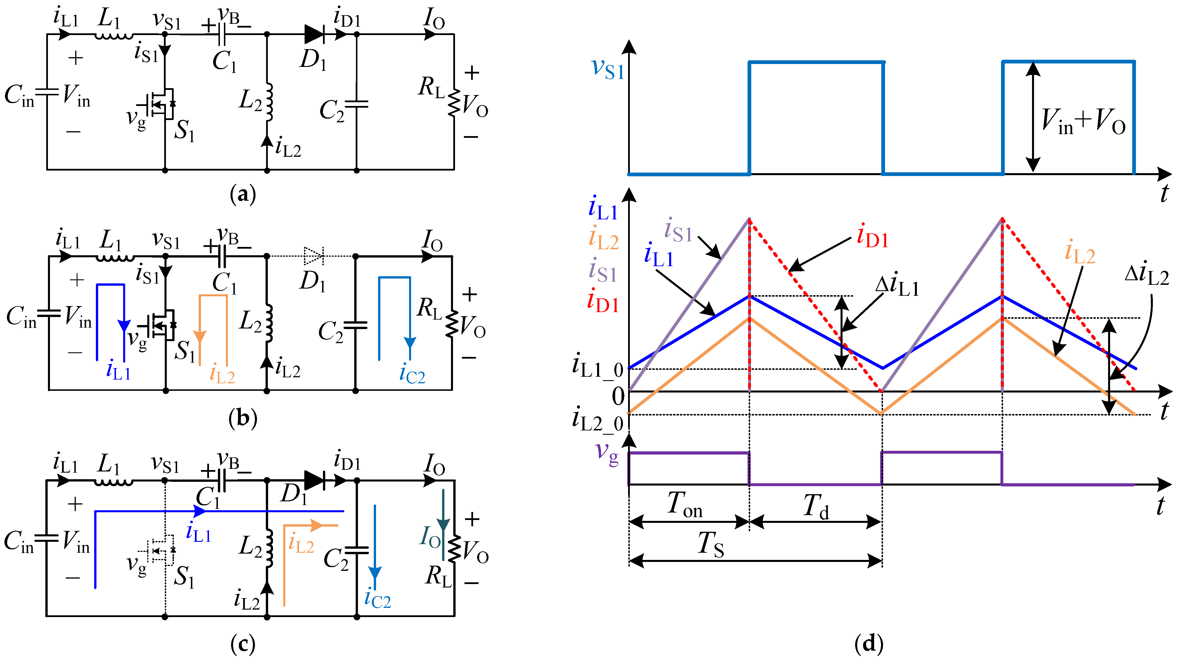
2. Boundary Conduction Mode SEPIC Power Factor Correction Converter with Constant-On-Time Control

Figure 1a presents the circuit diagram of SEPIC DC-DC converter topology, which is consisted of input capacitor Cin, inductors L1 and L2, main switch S1, freewheeling diode D1, middle capacitor C1, output capacitor C2 [38,39]. When the SEPIC converter operates at BCM mode, the SEPIC converter has two operation modes. Equivalent circuits of two operation modes and operation waveforms of the circuit are presented in Figure 1b–d.
Operation mode A: The main power switch S1 is switched on at the start of each switching cycle, diode D1 is reverse-biased, SEPIC converter works at operation mode A when S1 is on. Figure 1b,d shows the equivalent circuit and key waveforms for mode A. In operation mode A, the voltage of vS1 is zero because S1 is on; Cin, L1, and S1 form a current loop, the input voltage Vin applies to inductor L1, the inductor current iL1 ramps up with the slope of Vin/L1 from the initial value iL1_0; C1, S1, and L2 form a current loop, the middle capacitor voltage vB applies to inductor L2, the inductor current iL2 ramps up with the slope of vB/L2 from the initial value iL2_0; Output capacitor C2 and output load RL form a current loop, output capacitor C2 provides energy to load resistor; Both inductor currents of L1 and L2 flow through switch S1, the currents flowing through S1 ramp up from zero [38,39].
Operation mode B: When the turn-on time reaches the target value, S1 is turned off, operation mode A ends, and the converter enters operation mode B Figure 1c,d show the equivalent circuit and key waveforms for mode B. In operation mode B, S1 is turned off, and D1 is forward-biased, which makes both inductors L1 and L2 release energy to the middle capacitor C1 and output load through diode D1. In operation mode B, the voltage of vS1 is Vin + VO because D1 is forward-biased and vB is equal to Vin; Cin, L1, C1, D1, C2, and RL form a current loop, the output voltage VO applies to inductor L1, the inductor current iL1 decreases with the slope of VO/L1 from the peak value; L2, D1, C2, and RL form a current loop, the output voltage VO applies to inductor L2, the inductor current iL2 decreases with the slope of VO/L2 from the peak value; Both inductor currents of L1 and L2 flow through diode D1, when the current iD1 decreases to zero, S1 is turned on, the next switching cycle is started again [38,39].
The block diagram of the SEPIC PFC converter operating in BCM with the conventional COT control is presented in Figure 2a. It consists of rectifier bridge DRec, inductors L1 and L2, main switch S1, freewheeling diode D1, middle capacitor C1, output capacitor C2, error amplifier EA, comparator CMP, sawtooth generator, zero current detection, SR flip-flop etc. In addition, Lf and Cf are used as low-pass input filters.
Figure 2b presents the operation waveforms of the SEPIC PFC circuit working in BCM with traditional COT control during half AC line period. At the start of each switching cycle, S1 is turned on; when the voltage vSaw of the sawtooth generator at the positive input terminal of comparator CMP increases to Vcomp, S1 is turned off. According to Figure 2b, the output voltage Vcomp of the error amplifier maintains constant in half the AC line period because the bandwidth of the control loop is usually much lower than the AC line frequency for the PFC converter [34,35]. Furthermore, since the slope of the sawtooth generator of COT control is fixed, the on-time of S1 is almost fixed when the converter operates in a steady state with a stable input voltage and output load.
By analyzing the operation principle, the inductor current peak-to-peak ripple of L1 and L2 of SEPIC PFC converter operating in BCM can be given by
Δ i L 1 ( t ) = V M sin ( ω t ) T on L 1
Δ i L 2 ( t ) = v B ( t ) T on L 2
where VM and vB(t) is the amplitude of input voltage and the voltage of the middle capacitor C1 respectively, Ton is the on-time of S1. In the derivation of the following equation, iL1_0(t) and iL2_0(t) are the initial values of L1 and L2 currents for each switching cycle, respectively, iL1_avg(t) and iL2_avg(t) are the average values of the current flowing through L1 and L2.
During the steady operation, the average voltage of middle capacitor C1 in one switching cycle is equal to the rectified input voltage [33], so there is.
v B ( t ) = V M sin ( ω t )
Because the rectified input current is equal to the average current of the inductor L1, the input current iin(t) can be expressed as follows.
i in ( t ) = i L 1 _ avg ( t ) = i L 1 _ 0 ( t ) + Δ i L 1 ( t ) 2
The SEPIC converter operates in BCM. Once the current of D1 decreases to zero, S1 is turned on, and the initial current of main switch S1 should be zero, so there is.
i L 1 _ 0 ( t ) + i L 2 _ 0 ( t ) = 0
The charge balance of the middle capacitor C1 in a switching period can be expressed as
Δ i L 1 ( t ) 2 + i L 1 _ 0 ( t ) T d ( t ) = Δ i L 2 ( t ) 2 + i L 2 _ 0 ( t ) T on
where Td(t) is the time that diode D1 is forward biased, and Td(t) can be obtained as
T d ( t ) = V M sin ( ω t ) T on V O
According to (1), (2), (3), (5), (6), and (7), iL1_0(t) can be expressed as
i L 1 _ 0 ( t ) = T on V M sin ( ω t ) 2 V O + V M sin ( ω t ) V O L 2 V M sin ( ω t ) L 1
From (1), (4), and (8), the input current iin(t) can be obtained as
i in ( t ) = T on V M sin ( ω t ) 2 1 + K 1 sin ( ω t ) 1 L 1 + 1 L 2
where K1 = VM/VO.
Equation (9) shows that the input current is not an ideal sine-waveform. Therefore, with the traditional COT control, unity PF cannot be achieved except with extreme condition K1 = 0.

3. Variable-On-Time Control Scheme

Observing Equation (9), the denominator of the equation contains (1 + K1sin(ωt)), which prevents the input current from being sinusoidal. Based on (9), suppose Ton can be controlled to be proportional to (1 + K1sin(ωt)), the unity PF may be achieved. Figure 3 illustrates a detailed block diagram for the developed procedure from COT control to VOT control, which can explain how the VOT control with variable slope sawtooth generator is proposed.
By analyzing (9) and Figure 3, to realize sinusoidal input current, the on time of S1 is supposed as
T on ( t ) = K Ton 1 + K 1 sin ( ω t )
where KTon is a constant parameter about turning on the time control circuit. Combining (9) and (10), the input current can be written as
i in ( t ) = K Ton V M sin ( ω t ) 2 1 L 1 + 1 L 2
Observing (11), it can be seen that the ideal sinusoidal input current can be achieved if the on-time of S1 can be varied, as in equation (10).
Combing definition of K1 and SEPIC converter operation theory [38,39], Equation (10) can be written as
T on ( t ) = K Ton V O + V M sin ( ω t ) V O = K Ton D ( t )
D(t) is the duty cycle of S1. Based on Equation (12) and the turn-on time circuit of COT control, it is conceivable to use a variable slope sawtooth generator to produce variable turn-on time, as shown in Figure 3. The variable slope sawtooth generator consists of a charging current iCHG, a voltage-controlled current source (VCCS), a timing capacitor CT, a reference voltage source V1, a low pass RC filter comprised of R3 and C3, and three signal switches S2~S4 etc.
Therefore, using a variable slope sawtooth generator to produce variable turn-on time, a novel VOT control scheme for SEPIC PFC converter operating in BCM, which can get unity PF, is proposed. Figure 4 illustrates the block diagram and key operation waveforms of the SEPIC PFC converter operating in BCM with VOT control. Compared to the COT control strategy shown in Figure 2a, only an additional variable slope sawtooth generator, shown in the blue dashed line of Figure 4a, is required in the VOT control strategy.
According to the circuit of the variable slope sawtooth generator in Figure 4a, the signal switch S4 is controlled by gate drive signal Q of S1, and the signal switch S2 and S3 are controlled by the inverting drive signal Q. Hence, the turn-on time of the signal switches S4 and S3 are Ton(t) and Ts(t)-Ton(t) respectively. The low pass RC filter comprised of R3 and C3 filters out the switching frequency so that the control voltage vC3 of the VCCS remains stable during a switching period. Therefore, the charging current iCHG(t) of the sawtooth generator can be expressed by
i CHG ( t ) = g 1 v C 3 ( t ) = g 1 V 1 T on ( t ) T S ( t ) = g 1 V 1 D ( t )
where g1 is the control ratio of the VCCS iCHG, Ton(t), TS(t), and D(t) are the turn-on time, the switching period, and the duty cycle of S1 respectively. According to Equation (13) and Figure 4, the slope of the sawtooth generator in the proposed converter is variable with D(t) of S1. Therefore, the turn-on time of switch S1 can be expressed as
T on ( t ) = V comp C T i CHG ( t ) = V comp C T g 1 V 1 D ( t )
Since the SEPIC PFC converter operates in BCM, there are
T S ( t ) = T on ( t ) + T d ( t )
D ( t ) = T on ( t ) T S ( t )
According to (1), (2), (3), (5), (6), (7), (15), and (16), the initial inductor current iL1_0(t) of L1 for the proposed VOT control scheme can be obtained as
i L 1 _ 0 ( t )   = D ( t ) V M sin ( ω t ) T on ( t ) 2 1 L 2 1 L 1 V M sin ( ω t ) V O
From (1), (4), (17), the input current iin(t) with VOT control can be derived as
i in ( t ) = V M sin ( ω t ) T on ( t ) D ( t ) 2 1 L 1 + 1 L 2  
By substituting (14) into (18), the input current iin(t) with VOT control can be obtained as
i in ( t ) = V comp C T V M sin ( ω t ) 2 g 1 V 1 1 L 1 + 1 L 2  
During operating at a steady state, the error signal Vcomp keeps almost constant during half line period because of the quite narrow control loop bandwidth. For a given converter, the timing capacitor CT of the sawtooth generator and the control ratio g1 of the VCCS iCHG are constant. Therefore, define KTon in (11) as
K Ton = V comp C T g 1 V 1
According to (11), (19), and (20), Equations (11) and (19) are the same. Therefore, the input current with VOT control is an ideal sine-waveform. Hence the proposed VOT control scheme can achieve the theoretical unity PF of the SEPIC PFC converter operating in BCM.

4. Performance Comparison

4.1. Comparison of Input Current and Power Factor

According to (1), (2), and Figure 2, the peak current through D1 of COT control can be given as
i D 1   _ PK _ COT ( t ) = Δ i L 1 _ COT ( t ) + Δ i L 2 _ COT ( t ) = V M sin ( ω t ) T on _ COT ( 1 L 1 + 1 L 2 )
where Ton_COT is the turn-on time of S1 with COT control.
The average current flowing through D1 during each switching period with COT control can be derived as
i D 1 _ AVG _ COT ( t ) = i D 1 _ PK _ COT ( t ) T d _ COT ( t ) 2 T S _ COT ( t )
where Td_COT(t) and TS_COT(t) is the forward bias time of diode D1 and the switching period of COT control.
As the average current of diode D1 is equal to the output current IO in half line cycle, the output current IO with traditional COT control can be given as
I O = 1 π 0 π i D 1 _ AVG _ COT ( t ) d ( ω t )   = K 2 V M 2 T on _ COT 2 π V O ( 1 L 1 + 1 L 2 )
where
K 2 = 0 π sin 2 ( ω t ) ( 1 + K 1 sin ( ω t ) ) d ( ω t )
From (9) and (23), the input current of COT control can be obtained as
i in _ COT ( t ) = π V O I O sin ( ω t ) K 2 V M 1 + K 1 sin ( ω t )
In the same way, the input current of VOT control can be derived as
i in _ VOT ( t ) = 2 V O I O sin ( ω t ) V M
To conveniently compare the input currents of both control schemes, the normalized input currents with the base of (2VOIO)/VM can be expressed as
i in _ COT * ( t ) = π sin ( ω t ) 2 K 2 ( 1 + K 1 sin ( ω t ) )
i in _ VOT * ( t ) = sin ( ω t )
According to (27) and (28), Figure 5 shows both control schemes’ normalized input currents waveform with different K1 in half-line cycles. Observing Figure 5, the input current of the VOT control scheme is in shape with sinusoidal, but the input current waveform of COT control deviates from sinusoid, especially when K1 is large.
According to (25), the PF of COT control can be derived as
P F COT = 2 P in _ COT V M I in _ RMS _ COT = 2 0 π sin 2 ( ω t ) 1 + K 1 sin ( ω t ) d ( ω t ) π 0 π sin ( ω t ) 1 + K 1 sin ( ω t ) 2 d t
According to (26), (29), and the circuit parameters listed in Table 1 of Section 5, the comparison of the PF of COT and VOT control schemes with the variation of input voltage can be depicted in Figure 6. Therefore, it can be known that compared with COT control, the SEPIC PFC converter operating BCM with the proposed VOT control scheme based on variable slope sawtooth generator can improve the PF and realize theoretical unity PF.

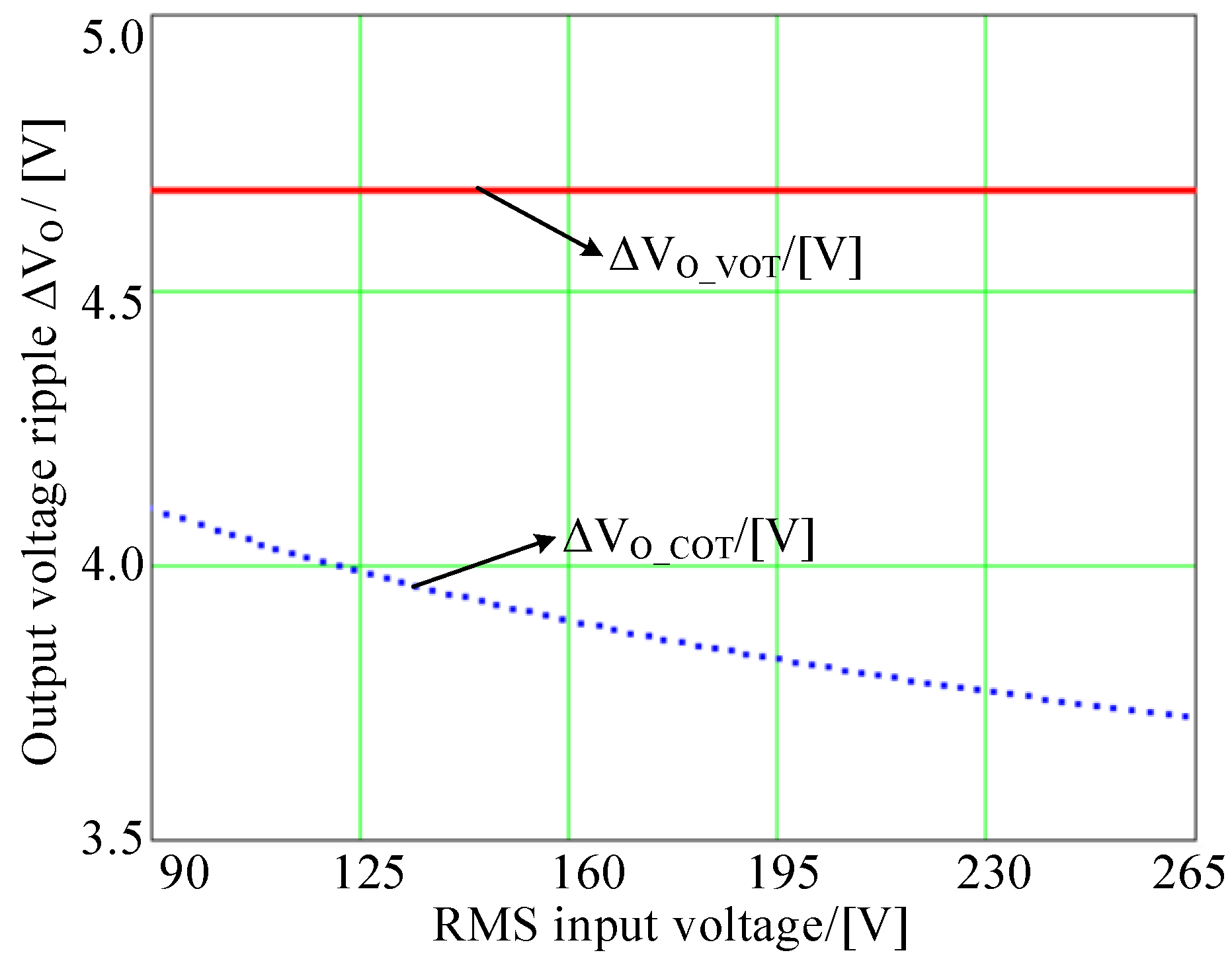
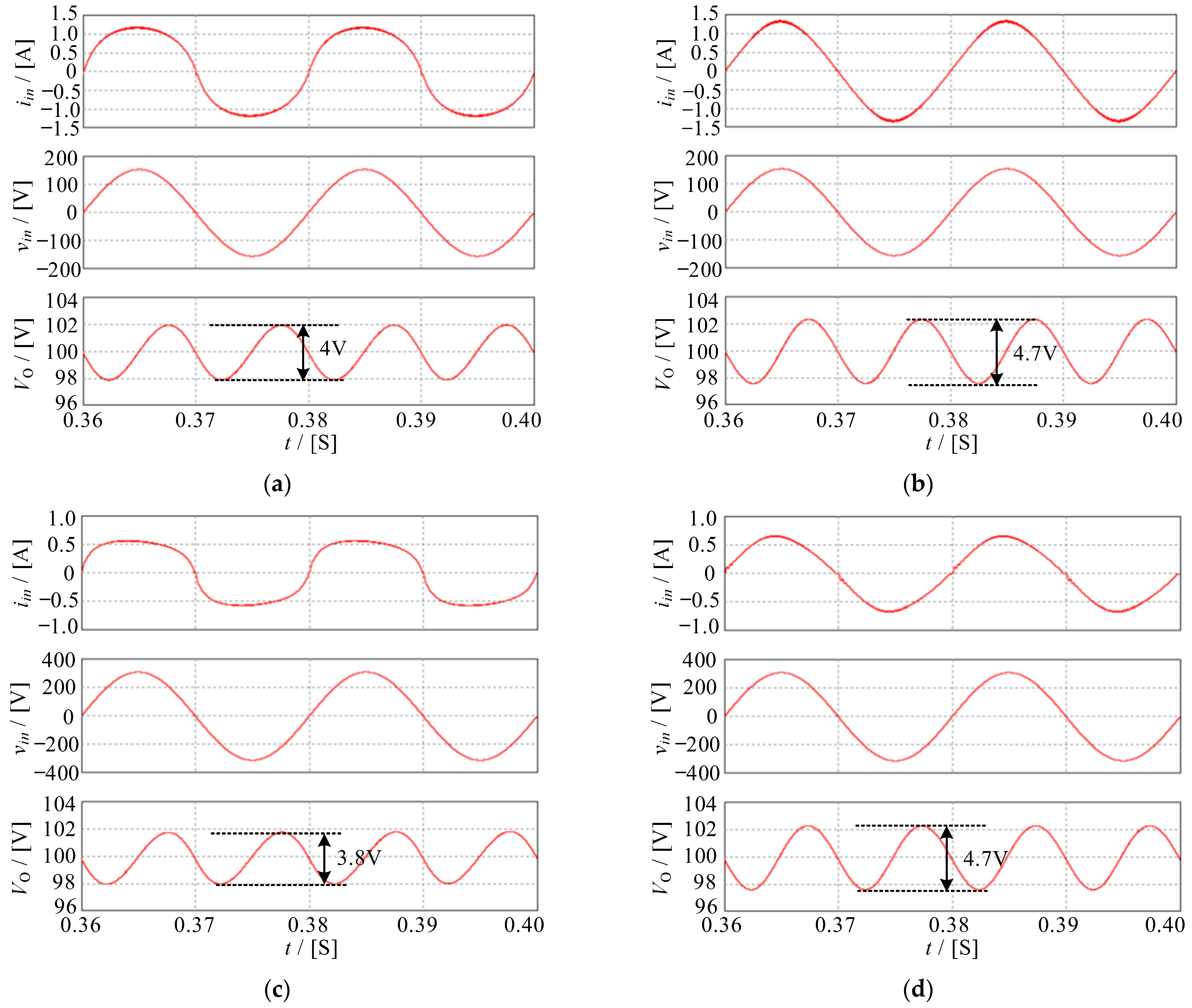
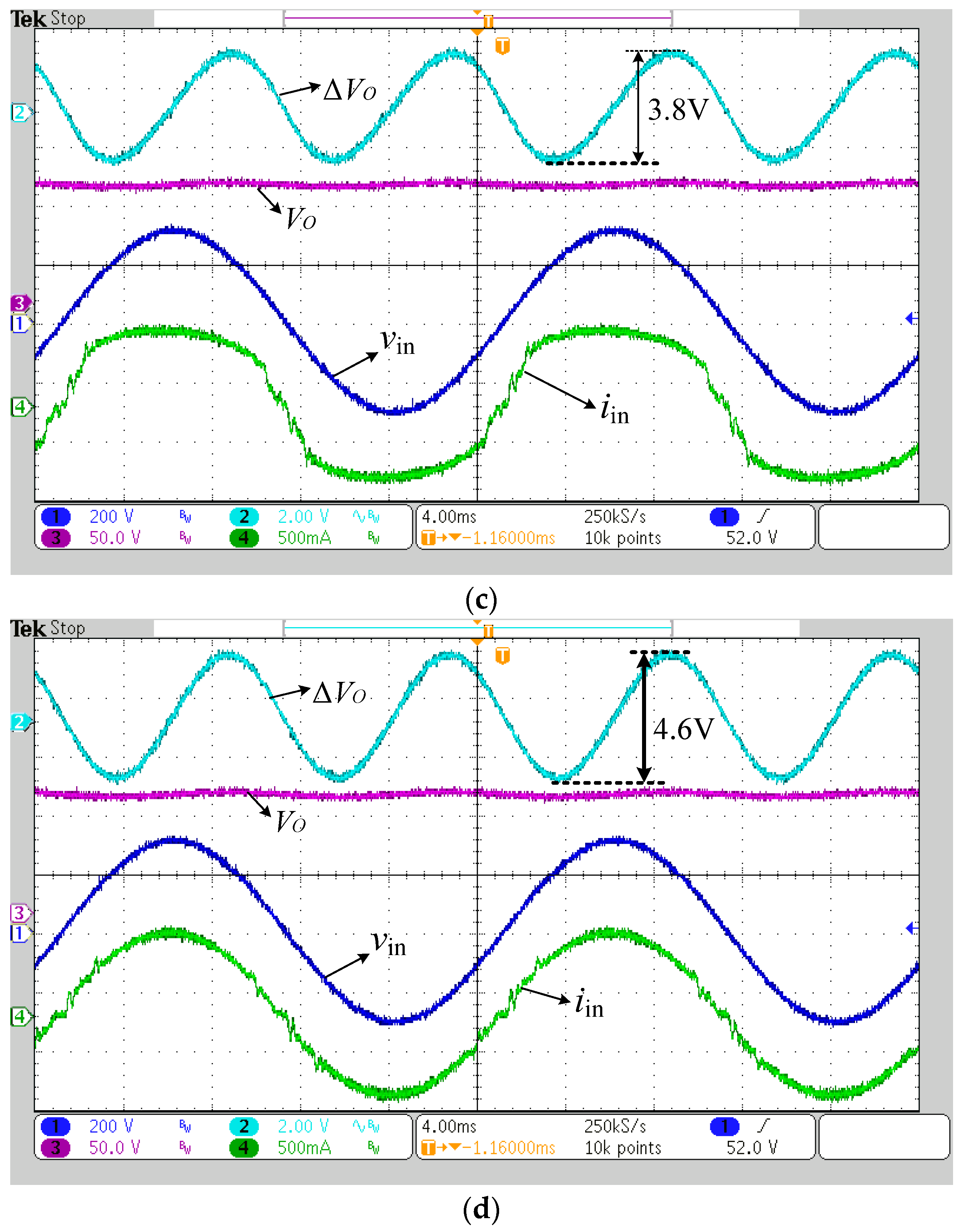
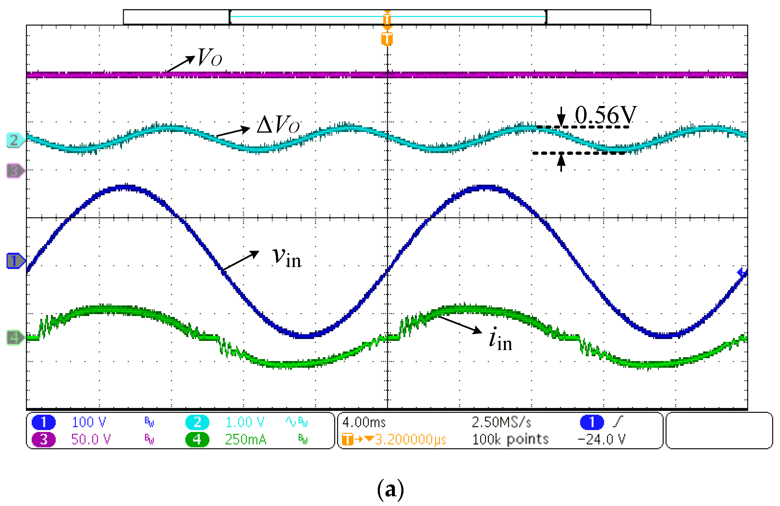
4.2. Comparison of Output Voltage Ripple

The instantaneous power imbalance between the output and input of the PFC converter leads to a double-line frequency ripple of output voltage [34]. By analyzing the circuit of Figure 2, the double line frequency output voltage ripple is produced by the second-order harmonic current of iD1 flowing into output capacitor C2.
According to the Fourier series formula, the second-order harmonic current’s magnitude of D1 with COT control, I D 1 _ COT 2 nd , can be derived as
I D 1 _ COT 2 nd = 2 π 0 π i D 1 _ AVG _ COT ( t ) cos ( 2 ω t ) d ( ω t )       = V M 2 T on _ COT π V O ( 1 L 1 + 1 L 2 ) 0 π sin 2 ( ω t ) cos ( 2 ω t ) ( 1 + K 1 sin ( ω t ) ) d ( ω t )              = K 3 I O
where
K 3 = 2 0 π sin 2 ( ω t ) ( 1 + K 1 sin ( ω t ) ) cos ( 2 ω t ) d ( ω t )    0 π sin 2 ( ω t ) ( 1 + K 1 sin ( ω t ) ) d ( ω t )
According to (23), (24), and (30), the output voltage ripple of COT can be derived as
Δ V O _ COT = I D 1 _ COT 2 nd 2 π f L C 2 = K 3 I O 2 π f L C 2
In the same way, the output voltage ripple of VOT can be presented as
Δ V O _ VOT = I O 2 π f L C 2
According to (32), (33), and the key parameters listed in Table 1 of Section 5, the output voltage ripple of both control schemes with different input voltage can be plotted in Figure 7. It can be known that compared with COT control, the output voltage ripple with the VOT control scheme is slightly larger.

4.3. Comparison of Switching Frequency

From (23), the turn-on time of S1 with COT control can be given as
T on _ COT = 2 π I O V O K 2 V M 2 ( 1 L 1 + 1 L 2 )
From (7) and (15), the switching frequency of COT can be derived as
f S _ COT ( t ) = K 2 V M 2 2 π V O I O ( 1 + K 1 sin ( ω t ) ) ( 1 L 1 + 1 L 2 )
In the same way, the turn-on time, and the switching frequency of S1 of VOT control can be given respectively as
T on _ VOT ( t ) = 4 V O I O ( 1 + K 1 sin ( ω t ) ) V M 2 ( 1 L 1 + 1 L 2 )  
f S _ VOT ( t ) = V M 2 4 V O I O ( 1 + K 1 sin ( ω t ) ) 2 ( 1 L 1 + 1 L 2 )
As the peak currents of the inductors L1 and L2 occur at ωt = π/2, it is important to analyze the switching frequencies of both control schemes at ωt = π/2 during designing both inductors L1 and L2. According to (35), (37), and the parameters listed in Table 1 of Section 5, the switching frequency of COT and VOT control at ωt = π/2 with the variation of RMS input voltage can be obtained in Figure 8.
From (35) and (37), with the base of V M 2 4 V O I O ( 1 L 1 + 1 L 2 ) , the normalized switching frequencies with both control schemes are derived as
f s _ COT * ( t ) = 2 K 2 π ( 1 + K 1 sin ( ω t ) )
f s _ VOT * ( t ) = 1 ( 1 + K 1 sin ( ω t ) ) 2
From (38) and (39), the normalized switching frequency variations curves with COT and VOT control schemes during half AC line period can be plotted in Figure 9.
Figure 8 shows that the switching frequency of both control schemes increases with the increase of the RMS value of input voltage at ωt = π/2. According to Figure 8 and Figure 9, with the same RMS input voltage, the switching frequency of VOT is lower than that of COT control when the transient input voltage is near the peak value, i.e., when ωt is π/2; the switching frequency of VOT is greater than that of COT when the transient input voltage is near the zero crossing. This is because the range of the VOT control’s switching frequency variation is wider than that of the COT control. Hence, compared with COT control, the cut-off frequency of the input low-pass filter of VOT control is lower. Moreover, to avoid extremely high switching frequency, both BCM SEPIC PFC converters with COT and VOT control schemes should limit the main power switch’s maximum switching frequency or minimum turning-off time.

4.4. Comparison of Peak Current of Main Switch

From the operation principle of SEPIC PFC converter operating in BCM, the peak currents of main switch S1 and freewheeling diode D1 are the same, so only the peak current of S1 is analyzed in this section.
According to (1), (2), (5), (34), and (36), the peak currents flowing through main switch S1 with COT and VOT control can be obtained as
i S 1 _ PK _ COT ( t ) = 2 π I O V O sin ( ω t ) K 2 V M
i S 1 _ PK _ VOT ( t ) = 4 I O V O sin ( ω t ) ( 1 + K 1 sin ( ω t ) ) V M
For the PFC converter, the peak current flowing through the main power switch S1 reaches a maximum when ωt is π/2. Therefore, according to (40), (41), and the key parameters listed in Table 1 of Section 5, the comparison of maximum peak currents flowing through S1 with both control schemes under different RMS input voltage can be depicted in Figure 10.
According to (40) and (41), with the base of (4IOVO)/VM, the peak current of main switch S1 with COT and VOT control is normalized as
i S 1 _ PK _ COT * ( t ) = π sin ( ω t ) 2 K 2
i S 1 _ PK _ VOT * ( t ) = sin ( ω t ) ( 1 + K 1 sin ( ω t ) )
According to (24), (42), and (43), the normalized peak current curve of S1 of COT and VOT control during half AC line period is depicted in Figure 11. It is indicated that for the same RMS input voltage, compared with COT control, the peak current flowing through S1 of VOT control is higher when the transient input voltage is close to the peak value, the peak current flowing through S1 of VOT control is smaller when the transient input voltage is near zero crossing.

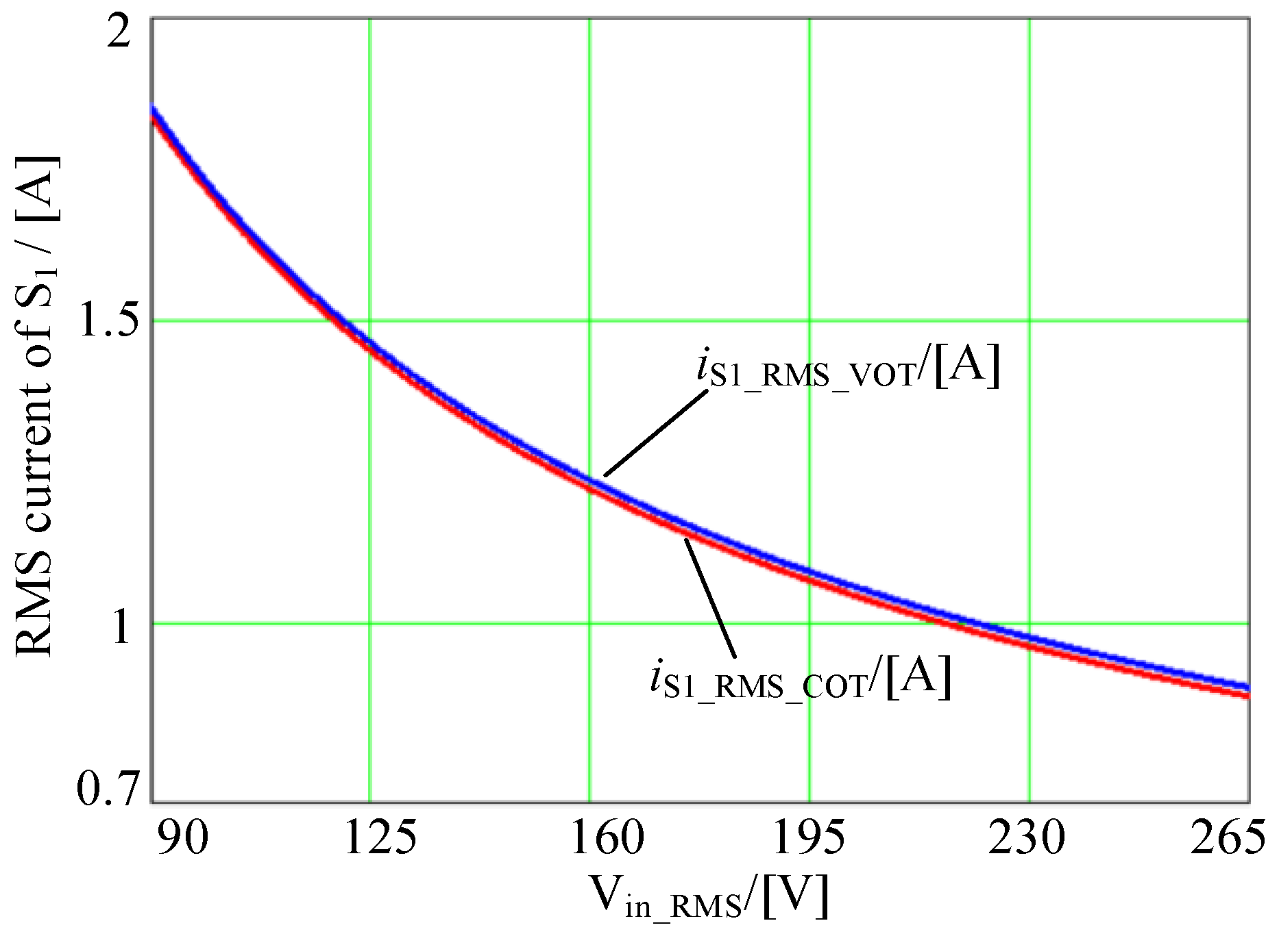
4.5. Comparison of RMS Current of Main Switch

According to (1), (2), (5), (7), and (34)–(37), the RMS current of S1 with COT and VOT control can be obtained as
I S 1 _ RMS _ COT = 1 π 0 π 0 T on _ COT ( V M sin ( ω t ) ( 1 L 1 + 1 L 2 ) u ) 2 d u T S _ COT ( t )    d ω t     = 2 I O V O V M π 3 K 2
I S 1 _ RMS _ VOT = 4 V O I O V M 0 π ( 1 + K 1 sin ( ω t ) ) sin 2 ( ω t )   d ω t 3 π
From (44), (45), and the key parameters listed in Table 1 of Section 5, the comparison of RMS currents of the main power switch with COT and VOT control under different RMS input voltages is given in Figure 12. Figure 12 shows that the RMS currents flowing through the main power switch with both control schemes are almost the same.
As mentioned above, when the instantaneous input voltage approaches the magnitude, the peak current flowing through S1 of COT control is smaller than that of VOT control, but the switching frequency of COT control is higher than that of VOT control; when the instantaneous input voltage approaches zero crossing point, the switching frequency of VOT control is higher than that of COT control, but the peak current of S1 of VOT control is smaller than that of COT control. Moreover, the RMS current of S1 of both control schemes is almost the same. Consequently, the power loss, including conduction loss and switching loss of the main power switch of both COT and VOT control, should be almost the same, and the efficiency of both control schemes should be almost the same.

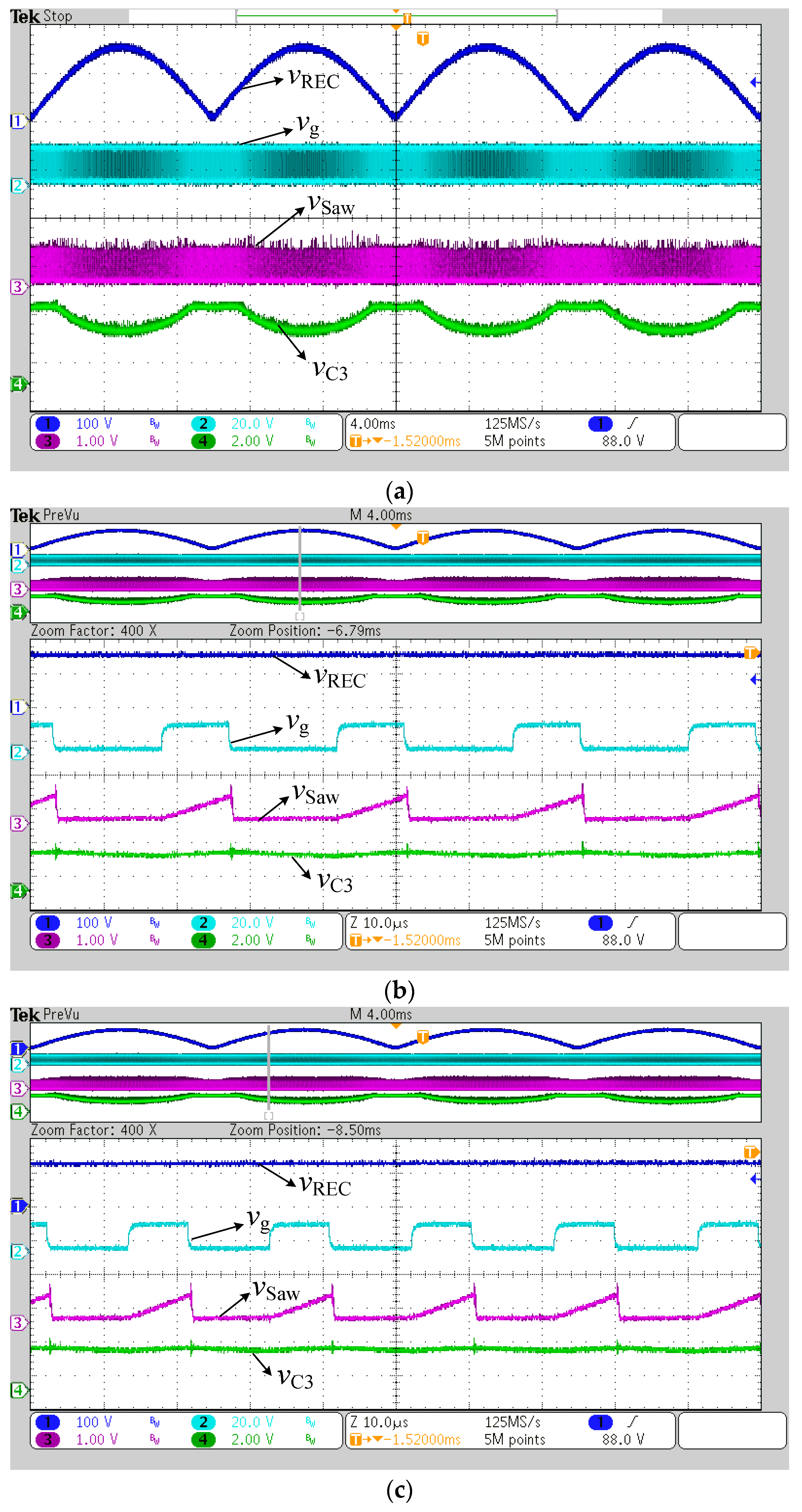
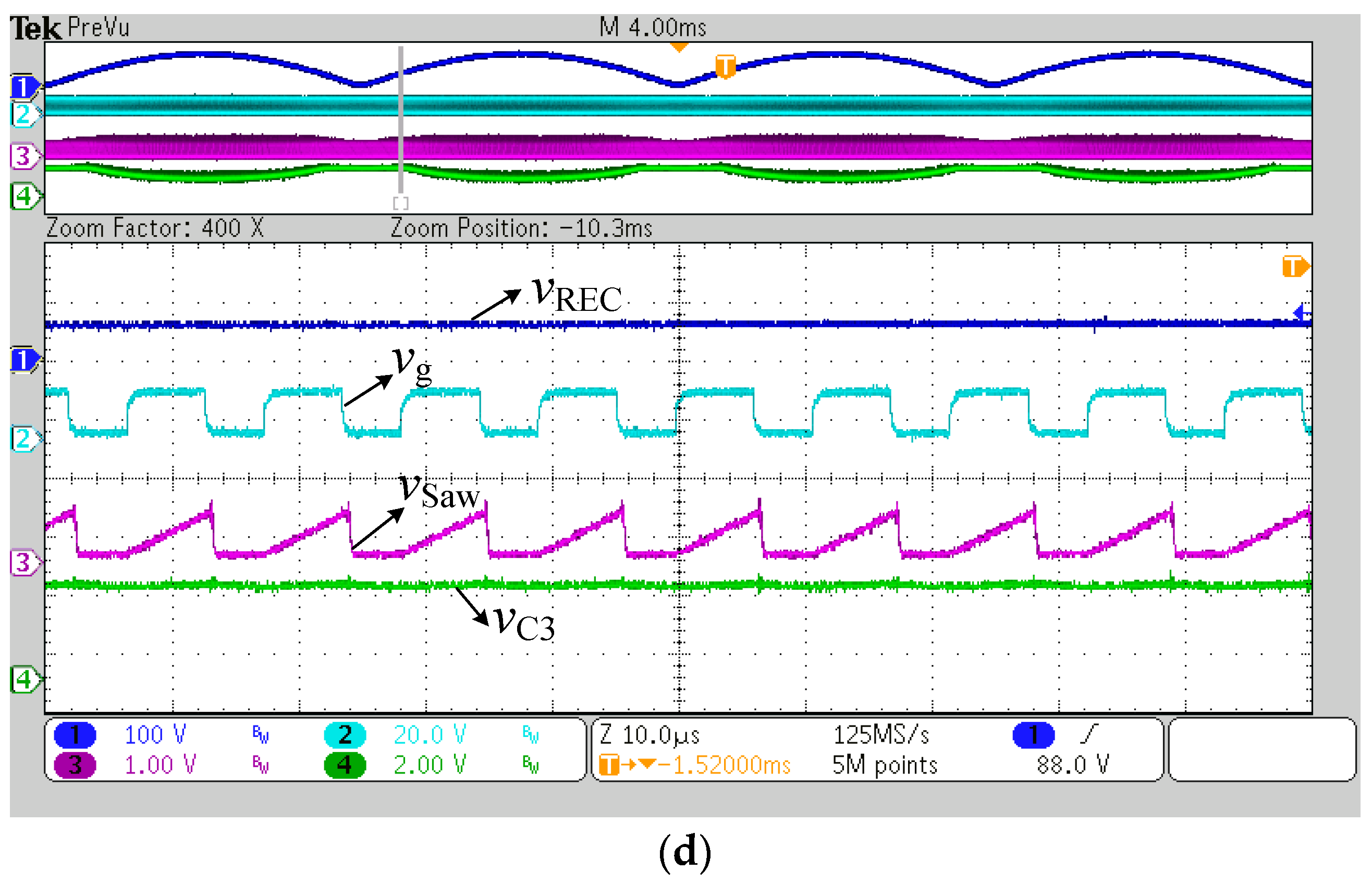
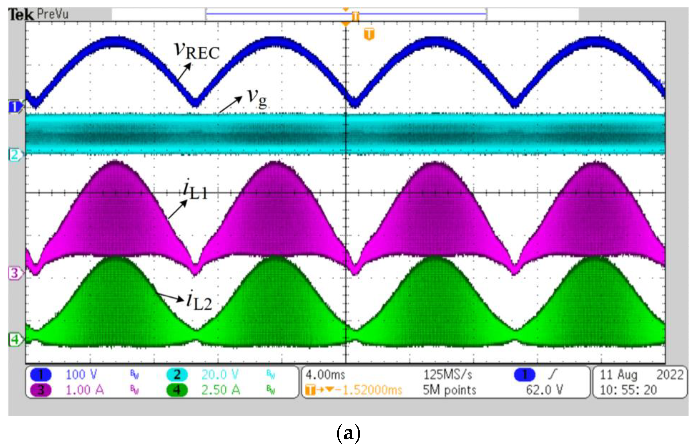
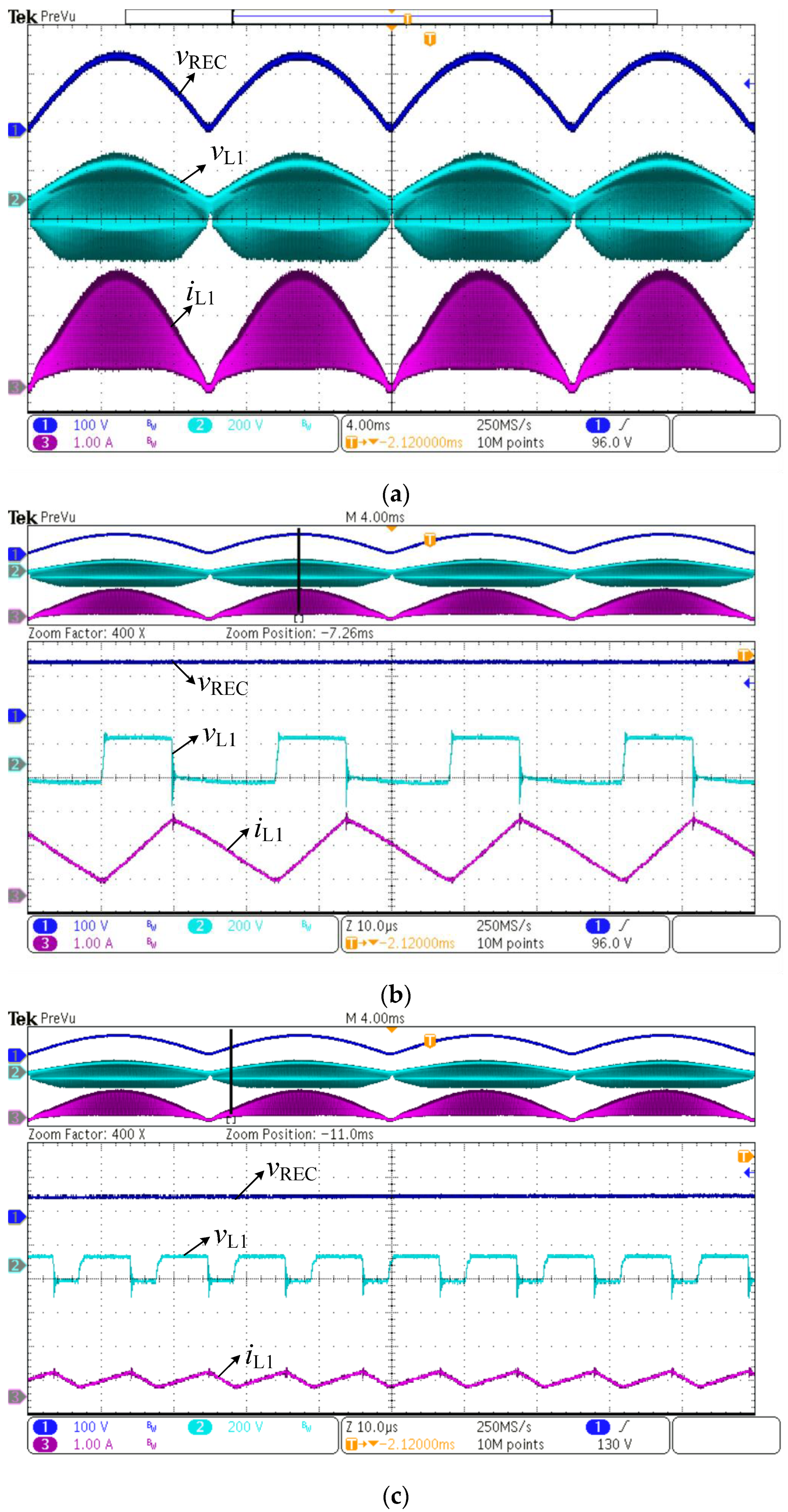
5. Analysis of Simulation and Experimental Results

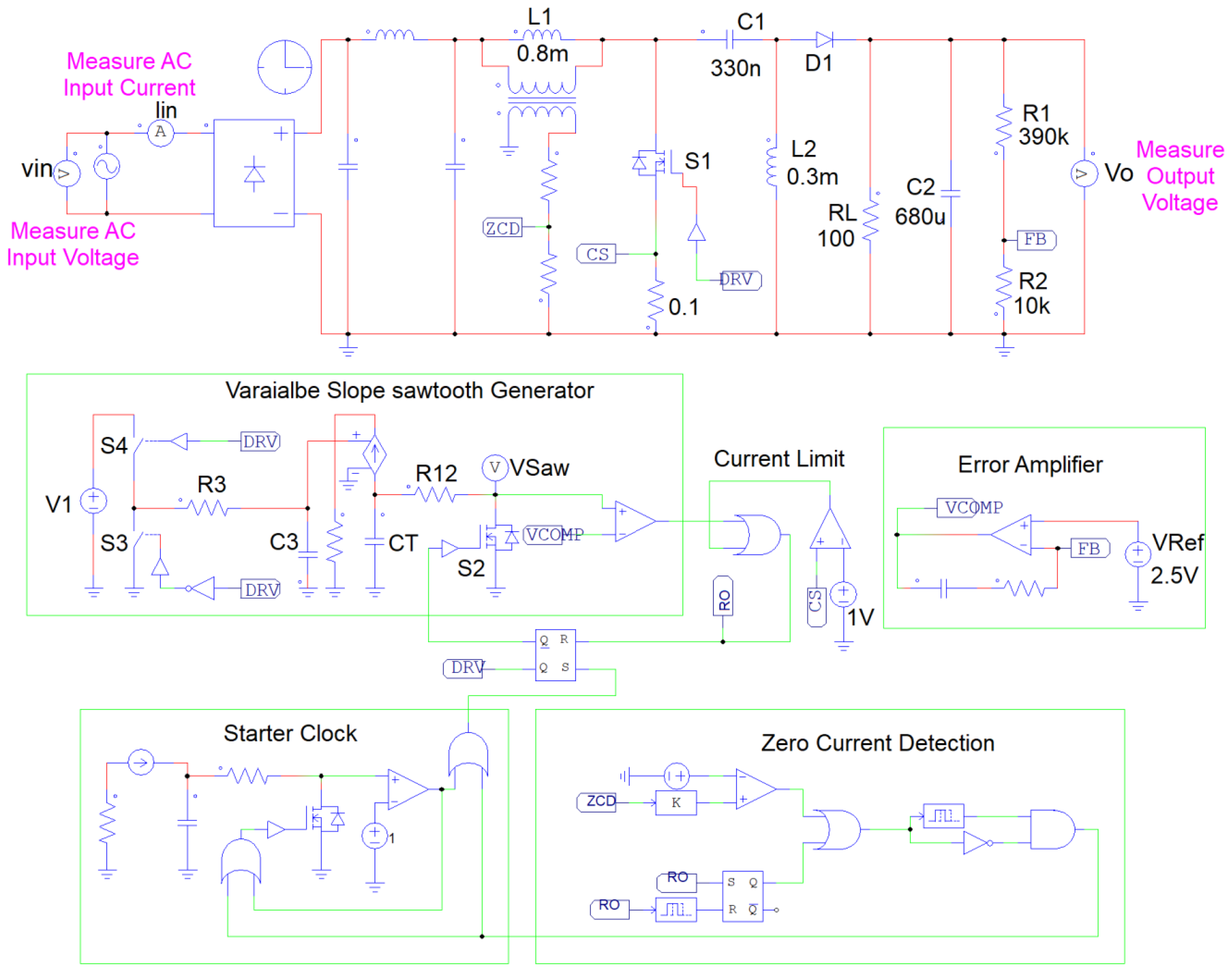
5.1. Analysis of Simulation Results

With the use of PSIM software, a simulation environment for power conversion and motor control, a computer simulation model shown in Figure 13 is designed to evaluate whether the VOT control of the SEPIC PFC converter operating at BCM is feasible. The specification and key circuit parameters are shown in Table 1. The differential probes are put at the AC input voltage terminal, and the output load terminal and the current probe are put in a series of AC input sources. After the RUN simulation model with PSIM, as shown in Figure 13, the simulation waveforms of input voltage, input current, and output voltage can be presented in Simview’s waveform windows of PSIM.
Table 1. Key Circuit Parameters.
Key ParametersVOT and COT
AC Input Voltage Range Vin_RMS90–265 V
Output Voltage VO100 V
Line Frequency fL50 Hz
Rated Output Current IO1 A
Output Filter Capacitor CO680 μF
Middle capacitor C11 μF
Inductor L1800 μH
Inductor L2300 μH
Main switch S1FCPF190N60
Freewheeling diode D1RHRP1560
Figure 14 gives the simulation waveforms of output voltage, input voltage, and input current at rated load current with 110 Vac and 220 Vac input voltage. As the simulation data indicates, the PF of COT with 110 Vac and 220 Vac is 0.991 and 0.977, respectively, while the PF of VOT with 110 Vac and 220 Vac is 0.999 and 0.995. The THD of COT when operating at 110 Vac and 220 Vac is 13.5% and 19.5%, respectively, while the THD of VOT when operating at 110 Vac and 220 Vac is 2.2% and 4.3%, respectively. The simulation results show that the input current of VOT is closer to the ideal sine-wave than that of COT, the THD of VOT is smaller than COT control, and the output voltage ripple of VOT is just a little larger than that of COT. The simulation results match the theoretical analysis results.

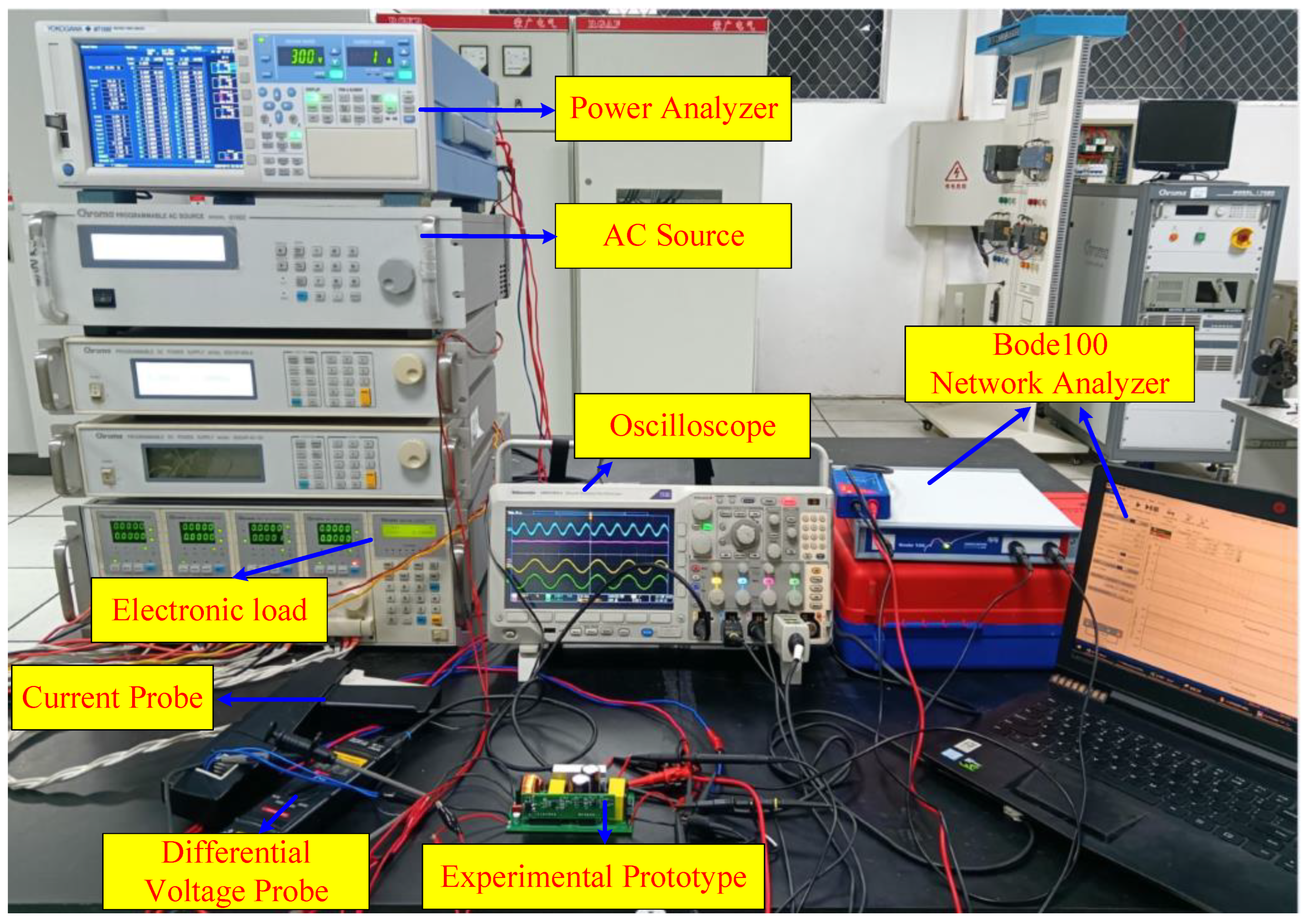
5.2. Experimental Results

The experimental verifications of both COT and VOT control methods are performed to prove the feasibility of the suggested VOT control for BCM SEPIC PFC converter and the theoretical performance comparison analysis results of both control schemes. The major parameters and specifications of the experimental board are shown in Table 1. The experimental prototype and platform are shown in Figure 15 and Figure 16, respectively. The block diagram of the experimental platform is presented in Figure 17. In the experimental platform, the programmable AC source Chroma 61602 provides an AC input voltage source to the BCM SEPIC PFC converter, the programmable electronic load Chroma 6314 A and 63,115 A provides the adjustable load for the SEPIC PFC converter, the power analyzer Yokogawa WT1800 measures the PF, THD, input current harmonic, and input power, the digital oscilloscope DPO3014 and its current and voltage probes measure voltage and current waveform of the SEPIC PFC converter, network analyzer Bode100 is used to test the loop stability of the converter.
The experimental comparison waveforms, including input current, output voltage with 110 Vac and 220 Vac input voltage and rated load, are shown in Figure 18a–d. The experimental comparison waveforms with 0.1 A and 0.5 A output load and 110 Vac input voltage are shown in Figure 19a–d. The input current waveforms of VOT control are more sinusoidal and nearly ideal sine-wave when compared to that of COT control, particularly with higher output power. With the rated load current, the output voltage ripple ΔVO of COT and VOT control with 110 Vac input voltage is 4 V and 4.6 V, respectively, ΔVO of COT and VOT control with 220 Vac input voltage is 3.8 V and 4.6 V, respectively, ΔVO of COT control is slightly smaller than that of VOT control, which is the same as the analysis result of Figure 7 and simulation result of Figure 14.
Figure 20a–d show the experimental waveforms of the sawtooth waveform vSaw, the control voltage vC3 of the VCCS, the rectified input voltage vREC, and gate driver signal vg of a main switch for the proposed VOT control with 110 Vac input voltage and rated output current. Figure 20b–d is the zoom-in waveforms of Figure 20a at different transient rectified input voltage. Comparing with Figure 20b–d, it can be known that with the transient rectified input voltage decreasing from peak to valley, the control voltage vC3 of the VCCS and the slope of the sawtooth generator increase, the turn-on time of S1 decreases, which is the same as the analysis result in Figure 4.
Figure 21 and Figure 22 show both inductor currents iL1 and iL2, the rectified input voltage vREC, and gate driver signal vg of the main switch of COT and VOT control with 110 Vac input voltage and rated output current. According to Figure 21b,c, it can be shown that the turn-on time of the main power switch S1 of COT control with different transient rectified input voltage is maintained at 8.8 μS. However, from Figure 22b,c, it can be shown that the turn-on time values of S1 of the proposed VOT control are 9.6 μS and 6.6 μS near the peak of the transient rectified input voltage and the zero-cross point of the input voltage, respectively. Therefore, it is verified that the turn-on time of S1 of COT control maintains constant, but the turn-on time of S1 of VOT control reduces with the transient rectified input voltage decreasing.
Figure 21b and Figure 22b show that the switching frequencies of COT and VOT control at ωt = π/2 are 44.5 kHz and 42 kHz, respectively, almost the same as the analysis result of (35), (37) and Figure 8. Figure 21c and Figure 22c show that the switching frequencies of COT and VOT control with 50 V transient rectified input voltage are 75.2 kHz and 91.7 kHz, respectively. Therefore, compared with COT control, the switching frequency of VOT control is lower when ωt is π/2, and the switching frequency of VOT control is higher when ωt is near zero, which is the same as the analysis result of Figure 9.
Figure 21b and Figure 22b also show that the maximum peak currents of S1 of COT and VOT control are 6.4 A and 7.3 A, respectively. Experimental results prove that the maximum peak currents of S1 of VOT control are slightly bigger than that of COT control, which almost matches the analysis result in Figure 10.
Figure 23 shows the experimental waveforms of the rectified input voltage vREC, L1 inductor current iL1, and L1 inductor voltage vL1 with VOT control at 110 Vac input voltage and rated output current. Figure 24 shows the experimental waveforms of the rectified input voltage vREC, L2 inductor current iL2, and L2 inductor voltage vL2 with VOT control at 110 Vac input voltage and rated output current. From Figure 23 and Figure 24, when the rectified input voltage is near 155 V and 50 V, the inductors’ L1 and L2 voltage is also around 155 V and 50 V, respectively. While S1 is switched on, the voltage of inductors L1 and L2 always maintain 100 V during S1 is turned off. Therefore, Figure 23 and Figure 24 can verify that the voltage of both inductors L1 and L2 are equal to the rectified input voltage when S1 is switched on, the voltage of both inductor L1 and L2 are equal to output voltage when S1 is turned off during the whole line period, which is the same as the operation theory analysis.
The bode diagram of the closed-loop gain of the whole system with the controller can be used to judge the stability of the PFC converter [40,41]. To analyze the stability, the bode diagram of the closed-loop gain of the SEPIC PFC prototype operating in BCM with VOT control is tested by network analyzer Bode 100. The loop gain test result with 110 Vac input voltage and rated output current load is shown in Figure 25. For the PFC converter, the bandwidth should be lower than 20 Hz. Otherwise, the twice-line frequency 100 Hz output voltage ripple will be coupled into the voltage control loop. As a result, the input current control signal becomes distorted, creating a third harmonic current in the input current [34,37,42]. The phase margin of the power converter should be bigger than 45° to ensure the converter’s stability [41,42,43,44]. According to Figure 25, it can be observed that the bandwidths, which is the frequency of 0 dB gain magnitude and the phase margin of the whole loop, which is the phase of 0 dB gain magnitude, are 13.26 Hz and around 90° respectively, so the proposed prototype can work stably.
To verify the performance with the variation of different input voltage, the experimental comparison results of efficiency, PF, and THD with COT and VOT control at 90~265 Vac input voltage and rated 1 A output current are presented in Figure 26. To verify the performance with the different load currents, the experimental comparison results of efficiency, PF, and THD of COT and VOT control with 110 Vac input voltage and 0.1~1 A output current are shown in Figure 27. From both figures, it can be shown that the PF of VOT control is higher than that of COT control, THD of VOT control is lower than that of COT control over the entire input voltage range and output load current range. Especially with higher output current load, the proposed VOT control scheme can almost achieve unity PF. From the above experimental data, the PF of the VOT control is enhanced significantly, the THD of the VOT control is reduced remarkably, and the efficiency of both controls is almost the same. Therefore, compared to COT control, VOT control enhances the performance of PF and THD without reducing efficiency.
The comparison results of IEC61000-3-2 Class C requirements and the input current harmonic of both control schemes with a rated output current, 110 Vac and 220 Vac input voltage, are shown in Figure 28. It shows that the input current harmonic of VOT control is lower than that of COT control. Although both control schemes can meet the harmonic standard limit of IEC61000-3-2 Class C, the VOT control scheme will be easier to meet the applications with stricter input current harmonic requirements.

6. Conclusions

To enhance the PF and decrease the THD of SEPIC PFC converter operating in BCM, a novel VOT control scheme which can almost realize unity PF is proposed. This novel VOT control scheme doesn’t need input voltage feedforward and multiplier circuits required by many PFC control strategies. The proposed VOT control scheme uses a simple and easy-to-implement variable slope sawtooth generator whose slope is controlled by the duty cycle of the main switch to modulate the turn-on time of the main switch. Based on performance analysis, simulation, and experiment comparison results of the 100 W prototype, it is verified that the proposed VOT control scheme with variable slope sawtooth generator remarkably enhances the performance of PF and THD without affecting the efficiency by contrast with the conventional COT control.

Author Contributions

Conceptualization, X.S. and W.C.; methodology, X.S., Q.L. and W.C.; formal analysis, X.S., W.C., Q.L. and Y.W.; validation, X.S., W.C. and Q.L.; investigation, X.S. and W.C.; writing—original draft preparation, X.S.; writing—review and editing, X.S., W.C., Q.L. and Y.W. All authors have read and agreed to the published version of the manuscript.

Funding

This work was supported by the National Natural Science Foundation of China under Grant No. 52077180.

Data Availability Statement

Not applicable.

Conflicts of Interest

The authors declare no conflict of interest.

Abbreviations

ACAlternating Current
BCMBoundary Conduction Mode
CCMContinuous Conduction Mode
COTConstant On-Time
DCDirect Current
DCMDiscontinuous Conduction Mode
PFCPower Factor Correction
PFPower Factor
RMSRoot Mean Square
SEPICSingle Ended Primary Inductor Converter
THDTotal Harmonic Distortion
VOTVariable On-Time
VCCSVoltage-Controlled Current Source

Notation

CCapacitance
D(t)The duty cycle of the main power switch S1
fLLine frequency of AC input power source
fS_COTSwitching frequency of COT control
fS_VOTSwitching frequency of VOT control
f*S_COTNormalized switching frequency of COT control
f*S_VOTNormalized switching frequency of VOT control
g1Control ratio of voltage-controlled current source iCHG
iCHGCharge current for capacitor CT
iD1Current flowing through diode D1
iD1_AVG_COTAverage current flowing through diode D1 with COT control
iD1_PK_COTPeak current flowing through diode D1 with COT control
I D 1 _ COT 2 nd Input current
iinThe amplitude of second-order harmonic current of D1 with COT control
iin_COTInput current with COT control
Iin_RMS_COTRMS value of input current with COT control
iin_VOTInput current with VOT control
i*in_COTNormalized input current with COT control
i*in_VOTNormalized input current with VOT control
iL1Current flowing through inductor L1
iL1_0Initial value of iL1 when the main switch S1 starts to turn on
iL1_avgThe average value of the current flowing through L1
iL2Current flowing through inductor L2
iL2_0Initial value of iL2 when the main switch S1 starts to turn on
IOOutput current of SEPIC PFC converter
iS1Current flowing through S1
iS1_PK_COTPeak current of S1 with COT control
iS1_PK_VOTPeak current of S1 with VOT control
i*S1_PK_COTNormalized peak current of S1 with COT control
i*S1_PK_VOTNormalized peak current of S1 with VOT control
IS1_RMS_COTRMS current of S1 with COT control
IS1_RMS_VOTRMS current of S1 with VOT control
LInductance
PFCOTPower factor with COT control
PFVOTPower factor with VOT control
Pin_COTInput power with COT control
RResistance
TdTime of diode D1 forward bias
Td_COTTime of diode D1 forward bias with COT control
TonTurn-on time of main power switch S1
Ton_COTTurn-on time of S1 with COT control
Ton_VOTTurn-on time of S1 with VOT control
TSSwitching period
TS_COTSwitching period with COT control
V1Voltage source V1 in variable slope sawtooth generator shown in Figure 4
vBVoltage of the middle capacitor C1
VcompOutput voltage of error amplifier
vC3The voltage of C3
vgDriving signal of S1
vinInput voltage
VMAmplitude of AC input power source
VOOutput voltage
vRECRectified AC input voltage
vSawThe voltage of sawtooth generator at the positive input terminal of comparator
ΔiL1Inductor current ripple of L1
ΔiL1_COTInductor current ripple of L1 with COT control
ΔiL2Inductor current ripple of L2
ΔVOOutput voltage ripple
ΔVO_COTOutput voltage ripple with COT control
ΔVO_VOTOutput voltage ripple with VOT control
ωAngular frequency of AC input power source

References

  1. Garcia, O.; Cobos, J.A.; Prieto, R.; Alou, P.; Uceda, J. Single phase power factor correction: A survey. IEEE Trans. Power Electron. 2003, 18, 749–755. [Google Scholar] [CrossRef] [Green Version]
  2. Singh, B.; Singh, B.N.; Chandra, A.; Al-Haddad, K.; Pandey, A.; Kothari, D.P. A review of single-phase improved power quality AC-DC converters. IEEE Trans. Ind. Electron. 2003, 50, 962–981. [Google Scholar] [CrossRef] [Green Version]
  3. Costa, P.J.S.; Font, C.H.I.; Lazzarin, T.B. A family of single-phase voltage-doubler high-power-factor SEPIC rectifiers operating in DCM. IEEE Trans. Power Electron. 2017, 32, 4279–4290. [Google Scholar] [CrossRef]
  4. Limits for Harmonic Current Emissions (Equipment Input Current ≤16 A per Phase); International Electrotechnical Commission Standard 61000-3-2; Electromagnetic Compatibility (EMC): Luxembourg, 2009.
  5. IEEE Recommended Practices and Requirements for Harmonics Control in Electric Power Systems; IEEE Standard 519; IEEE: Piscataway, NJ, USA, 2014.
  6. Wu, X.; Yang, J.; Zhang, J.; Qian, Z. Variable on-time (VOT)-controlled critical conduction mode buck PFC converter for high-input AC/DC HB-LED lighting applications. IEEE Trans. Power Electron. 2012, 27, 4530–4539. [Google Scholar] [CrossRef]
  7. Liu, X.; Wan, Y.; He, M.; Zhou, Q.; Meng, X. Buck-type single-switch integrated PFC converter with low total harmonic distortion. IEEE Trans. Ind. Electron. 2021, 68, 6859–6870. [Google Scholar] [CrossRef]
  8. Yao, K.; Ruan, X.; Mao, X.; Ye, Z. Variable-duty-cycle control to achieve high input power factor for DCM boost PFC converter. IEEE Trans. Ind. Electron. 2011, 58, 1856–1865. [Google Scholar] [CrossRef]
  9. Chen, Y.L.; Chen, Y.M. Line current distortion compensation for DCM/CRM Boost PFC converters. IEEE Trans. Power Electron. 2016, 31, 2026–2038. [Google Scholar] [CrossRef]
  10. Frivaldsky, M.; Pipiska, M.; Spanik, P. Evaluation of the perspective power transistor structures on efficiency performance of PFC circuit. Electronics 2021, 10, 1571. [Google Scholar] [CrossRef]
  11. Chen, J.; Maksimovic, D.; Erickson, R.W. Analysis and design of a low-stress buck-boost converter in universal-input PFC applications. IEEE Trans. Power Electron. 2006, 21, 320–329. [Google Scholar] [CrossRef]
  12. Bist, V.; Singh, B. An adjustable-speed PFC bridgeless Buck–Boost converter-fed BLDC motor drive. IEEE Trans. Ind. Electron. 2014, 61, 2665–2677. [Google Scholar] [CrossRef]
  13. Brkovic, M.; Cuk, S. Automatic current shaper with fast output regulation and soft-switching. In Proceedings of the Intelec 93: 15th International Telecommunications Energy Conference, Paris, France, 27–30 September 1993; pp. 379–386. [Google Scholar]
  14. Pandey, R.; Singh, B. A power-factor-corrected LLC resonant converter for electric vehicle charger using Cuk converter. IEEE Trans. Ind. Appl. 2019, 55, 6278–6286. [Google Scholar] [CrossRef]
  15. Elkhateb, A.; Rahim, N.A.; Selvaraj, J.; Uddin, M.N. Fuzzy-logic-controller-based SEPIC converter for maximum power point tracking. IEEE Trans. Ind. Appl. 2014, 50, 2349–2358. [Google Scholar] [CrossRef]
  16. Durgadevi, S.; Umamaheswari, M.G. Analysis and design of single phase power factor correction with DC–DC SEPIC Converter for fast dynamic response using genetic algorithm optimised PI controller. IET Circ. Devices Syst. 2018, 12, 164–174. [Google Scholar] [CrossRef]
  17. Munuswamy, R.; Govindarajan, U.; Anbukumar, K. Performance comparison and stability analysis of ACM and ENLC controlled SEPIC PFC converter. IET Power Electron. 2020, 13, 991–1001. [Google Scholar] [CrossRef]
  18. Kanaan, H.Y.; Al-Haddad, K.; Sauriole, G.; Chaffai, R. Practical design of a SEPIC power factor corrector with DC-voltage regulation. In Proceedings of the 2006 IEEE International Symposium on Industrial Electronics, Montreal, QC, Canada, 9–13 July 2006; pp. 964–969. [Google Scholar]
  19. Burgardt, I.; Agostini, E.; Font, C.H.I.; Nascimento, C.B. Dimmable flicker-free power LEDs lighting system based on a SEPIC rectifier using a regenerative snubber. IET Power Electron. 2016, 9, 891–899. [Google Scholar] [CrossRef]
  20. Tian, G.; Qi, W.; Yan, Y.; Jiang, Y. High power factor LED power supply based on SEPIC converter. Electron. Lett. 2014, 50, 1866–1868. [Google Scholar] [CrossRef]
  21. Shi, C.; Wang, H.; Dusmez, S.; Khaligh, A. A SiC-Based high-efficiency isolated onboard PEV charger with ultrawide DC-link voltage range. IEEE Trans. Ind. Appl. 2017, 53, 501–511. [Google Scholar] [CrossRef]
  22. Gopalarathnam, T.; Toliyat, H.A. A new topology for unipolar brushless DC motor drive with high power factor. IEEE Trans. Power Electron. 2003, 18, 1397–1404. [Google Scholar] [CrossRef]
  23. Singh, B.; Singh, S. Single-phase power factor controller topologies for permanent magnet brushless DC motor drives. IET Power Electron. 2010, 3, 147–175. [Google Scholar] [CrossRef]
  24. Chiu, H.; Lo, Y.; Chen, J.; Cheng, S.; Lin, C.; Mou, S. A High-Efficiency Dimmable LED Driver for Low-Power Lighting Applications. IEEE Trans. Ind. Electron. 2010, 57, 735–743. [Google Scholar] [CrossRef]
  25. Pandey, R.; Singh, B. PFC-SEPIC converter-fed half-bridge LLC resonant converter for e-bike charging applications. IET Electr. Syst. Transp. 2020, 10, 225–233. [Google Scholar] [CrossRef]
  26. Kwon, J.M.; Choi, W.Y.; Lee, J.J.; Kim, E.H.; Kwon, B.H. Continuous-conduction-mode SEPIC converter with low reverse-recovery loss for power factor correction. IEE Proc. Electr. Power Appl. 2006, 153, 673–681. [Google Scholar] [CrossRef] [Green Version]
  27. Ye, Z.; Greenfeld, F.; Liang, Z. Offline SEPIC converter to drive the high brightness white LED for lighting applications. In Proceedings of the 2008 34th Annual Conference of IEEE Industrial Electronics, Orlando, FL, USA, 3 April 2008; pp. 1994–2000. [Google Scholar]
  28. Shi, C.; Khaligh, A.; Wang, H. Interleaved SEPIC power factor preregulator using coupled inductors in discontinuous conduction mode with wide output voltage. IEEE Trans. Ind. Appl. 2016, 52, 3461–3471. [Google Scholar] [CrossRef]
  29. Bianchin, C.G.; Gules, R.; Badin, A.A.; Romaneli, E.F.R. High-Power-Factor rectifier using the modified SEPIC converter operating in discontinuous conduction mode. IEEE Trans. Power Electron. 2015, 30, 4349–4364. [Google Scholar] [CrossRef]
  30. Jassim, B.M.H. SEPIC AC-DC converter for aircraft application. In Proceedings of the MELECON 2014—2014 17th IEEE Mediterranean Electrotechnical Conference, Beirut, Lebanon, 13–16 April 2014; pp. 12–16. [Google Scholar]
  31. Ye, Z.; Greenfeld, F.; Liang, Z. Design consideration of a high power factor SEPIC converter for high brightness white LED lighting applications. In Proceedings of the 2008 IEEE Power Electronics Specialists Conference, Rhodes, Greece, 15–19 June 2008; pp. 2657–2663. [Google Scholar]
  32. Simonetti, D.S.L.; Sebastian, J.; Uceda, J. The discontinuous conduction mode Sepic and Cuk power factor preregulators: Analysis and design. IEEE Trans. Ind. Electron. 1997, 44, 630–637. [Google Scholar] [CrossRef] [Green Version]
  33. Chen, J.; Chang, C. Analysis and design of SEPIC converter in boundary conduction mode for universal-line power factor correction applications. In Proceedings of the 2001 IEEE 32nd Annual Power Electronics Specialists Conference, Vancouver, BC, Canada, 17–21 June 2001; pp. 742–747. [Google Scholar]
  34. Yan, T.; Xu, J.; Zhang, F.; Sha, J.; Dong, Z. Variable-on-time-controlled critical-conduction-mode Flyback PFC converter. IEEE Trans. Ind. Electron. 2014, 61, 6091–6099. [Google Scholar] [CrossRef]
  35. Memon, A.H.; Yao, K.; Chen, Q.; Guo, J.; Hu, W. Variable-On-Time control to achieve high input power factor for a CRM-integrated Buck–Flyback PFC converter. IEEE Trans. Power Electron. 2017, 32, 5312–5322. [Google Scholar] [CrossRef]
  36. Wang, Y.; Zhang, Y.; Mo, Q.; Chen, M.; Qian, Z. An improved control strategy based on multiplier for CRM Flyback PFC to reduce line current peak distortion. In Proceedings of the 2010 IEEE Energy Conversion Congress and Exposition, Atlanta, GA, USA, 12–16 September 2010; pp. 901–905. [Google Scholar]
  37. Shen, X.; Yan, T.; Li, Q.; Wang, Y.; Chen, W. Variable on-time controlled boundary conduction mode single-ended primary inductor converter power factor correction converter. Electron. Lett. 2018, 54, 97–99. [Google Scholar] [CrossRef]
  38. Falin, J. Designing DC/DC Converters Based on SEPIC Topology. Available online: https://www.ti.com/lit/an/slyt309/slyt309.pdf (accessed on 9 February 2023).
  39. Zhang, D. AN-1484 Designing a SEPIC Converter. Available online: https://www.ti.com/lit/an/snva168e/snva168e.pdf (accessed on 9 February 2023).
  40. Zhang, R.; Liu, S.; Li, B.; Zhao, N.; Wang, G.; Xu, D. Totem-Pole bridgeless Boost PFC converter based on GaN HEMT for air conditioning applications. In Proceedings of the 2018 2nd IEEE Conference on Energy Internet and Energy System Integration (EI2), Beijing, China, 20–22 October 2018; pp. 1–9. [Google Scholar]
  41. Wei, Y.; Luo, Q.; Wang, J.; Sun, P. Analysis and design of the DCM operation boost PFC converter with magnetic control. IET Power Electron. 2019, 12, 3697–3706. [Google Scholar] [CrossRef]
  42. Schonberger, J. Modeling a PFC Controller Using PLECS. Available online: https://www.plexim.com/sites/default/files/plecs_pfc.pdf (accessed on 9 February 2023).
  43. Sahin, M.E.; Okumus, H.I. Comparison of different controllers and stability analysis for photovoltaic powered Buck-Boost DC-DC converter. Electr. Power Compon. Syst. 2018, 46, 149–161. [Google Scholar] [CrossRef]
  44. Sahin, M.E.; Okumus, H.I.; Aydemir, M.T. Implementation of an electrolysis system with DC/DC synchronous buck converter. Int. J. Hydrogen Energy 2014, 39, 6802–6812. [Google Scholar] [CrossRef]
Figure 1. The circuit diagram, equivalent circuits, and key waveforms of BCM SEPIC DC-DC converter. (a) Circuit diagram of SEPIC DC-DC converter topology; (b) Equivalent circuit when S1 is on; (c) Equivalent circuit when S1 is off; (d) Key waveforms during a switching cycle.
Electronics 12 01807 g001
Figure 2. Block diagram and main waveforms of SEPIC PFC converter operating in BCM with the traditional COT control scheme. (a) Block diagram; (b) Key waveforms during half AC line period.
Electronics 12 01807 g002
Figure 3. Block diagram for the developed procedure from COT control to VOT control.
Electronics 12 01807 g003
Figure 4. Block diagram and main waveforms of BCM SEPIC PFC converter with VOT control. (a) Block diagram; (b) Key waveforms during half line cycle.
Electronics 12 01807 g004
Figure 5. Comparison of the normalized input current waveform.
Electronics 12 01807 g005
Figure 6. Comparison of the PF with different RMS input voltage.
Electronics 12 01807 g006
Figure 7. Comparison of the output voltage ripple with the variation of RMS input voltage.
Electronics 12 01807 g007
Figure 8. Comparison of the switching frequency at ωt = π/2 with different input voltage.
Electronics 12 01807 g008
Figure 9. Comparison of the normalized switching frequency curves with COT and VOT control schemes during half AC line period.
Electronics 12 01807 g009
Figure 10. Comparison of the maximum peak current of S1 under different RMS input voltage.
Electronics 12 01807 g010
Figure 11. Comparison of the normalized peak current curves of S1 with COT and VOT control during half line cycle.
Electronics 12 01807 g011
Figure 12. RMS currents of the main switch with VOT and COT control under different RMS input voltage.
Electronics 12 01807 g012
Figure 13. Simulation model of SEPIC PFC converter operating in BCM with VOT control.
Electronics 12 01807 g013
Figure 14. Simulation waveforms at rated load current with 110 Vac and 220 Vac input voltage. (a) COT with 110 Vac; (b) VOT with 110 Vac; (c) COT with 220 Vac; (d) VOT with 220 Vac.
Electronics 12 01807 g014
Figure 15. Experimental Prototype.
Electronics 12 01807 g015
Figure 16. Experimental Platform.
Electronics 12 01807 g016
Figure 17. Block diagram of the experimental platform.
Electronics 12 01807 g017
Figure 18. Experimental waveforms of ΔVO, VO, vin, and iin with rated output current, 110 Vac and 220 Vac input voltage. (a) COT with 110 Vac; (b) VOT with 110 Vac; (c) COT with 220 Vac; (d) VOT with 220 Vac.
Electronics 12 01807 g018aElectronics 12 01807 g018b
Figure 19. Experimental waveforms of ΔVO, VO, vin, and iin with 110 Vac input voltage, 0.1 A and 0.5 A output current. (a) COT with 0.1 A output current; (b) VOT with 0.5 A output current; (c) COT with 0.5 A output current; (d) VOT with 0.5 A output current.
Electronics 12 01807 g019aElectronics 12 01807 g019b
Figure 20. Experimental waveforms of vREC, vg, vSaw, and vC3 of VOT control with 110 Vac input voltage and rated output current. (a) overall waveform; (b) zoom in waveform at ωt = π/2; (c) zoom in waveform at 120 V transient rectified input voltage; (d) zoom in waveform near zero-cross point of input voltage.
Electronics 12 01807 g020aElectronics 12 01807 g020b
Figure 21. Experimental waveforms of vREC, vg, iL1, and iL2 of COT control with 110 Vac input voltage and rated output current. (a) overall waveform; (b) zoomed-in waveform at ωt = π/2, i.e., vRec is 155 V; (c) zoomed-in waveform around zero-cross point of input voltage, vRec is 50 V.
Electronics 12 01807 g021aElectronics 12 01807 g021b
Figure 22. Experimental waveforms of vREC, vg, iL1, and iL2 of VOT control with 110 Vac input voltage and rated current load. (a) overall waveform; (b) zoomed-in waveform at ωt = π/2, i.e., vRec is 155 V; (c) zoomed-in waveform around zero-cross point of input voltage, vRec is 50 V.
Electronics 12 01807 g022aElectronics 12 01807 g022b
Figure 23. Experimental waveforms of vREC, vL1, and iL1 of VOT control with 110 Vac input voltage and rated current load. (a) overall waveform; (b) zoomed-in waveform at ωt = π/2, i.e., vRec is 155 V; (c) zoomed-in waveform around zero-cross point of input voltage, vRec is 50 V.
Electronics 12 01807 g023
Figure 24. Experimental waveforms of vREC, vL2, and iL2 of VOT control with 110 Vac input voltage and rated current load. (a) overall waveform; (b) zoomed-in waveform at ωt = π/2, i.e., vRec is 155 V; (c) zoomed-in waveform around zero-cross point of input voltage, vRec is 50 V.
Electronics 12 01807 g024
Figure 25. Loop gain test result of VOT control scheme with 110 Vac and rated output current load.
Electronics 12 01807 g025
Figure 26. Experimental comparison of PF, Efficiency, and THD data with 90~265 Vac input voltage and rated 1 A output current. (a) PF and efficiency; (b) THD.
Electronics 12 01807 g026
Figure 27. Experimental comparison of PF, Efficiency, and THD data with 0.1~1 A output current and 110 Vac input voltage. (a) PF and efficiency; (b) THD.
Electronics 12 01807 g027
Figure 28. Input current harmonic content comparison data with rated 1 A output current. (a) 110 Vac input voltage; (b) 220 Vac input voltage.
Electronics 12 01807 g028
Disclaimer/Publisher’s Note: The statements, opinions and data contained in all publications are solely those of the individual author(s) and contributor(s) and not of MDPI and/or the editor(s). MDPI and/or the editor(s) disclaim responsibility for any injury to people or property resulting from any ideas, methods, instructions or products referred to in the content.

