1. Introduction
In the literature, power amplifiers may be classified into two types: CW (Continuous Microwave) power amplifiers and pulsed power amplifiers [
1,
2,
3]. The power of the most recent X-band high-power pulsed power amplifiers has reached the kW level due to material advancement and structure optimization [
4]. However, in order to reduce heat dissipation and ensure safety, high-power power amplifiers should operate in pulse mode [
5]. To obtain more efficiency, greater output power, and higher gain, designers of high-power amplifiers often prefer employing drain modulation rather than gate modulation [
6,
7]. The microwave pulse is fully nested in the drain voltage pulse to ensure the quality of the microwave waveform when using drain bias modulation. According to the literature [
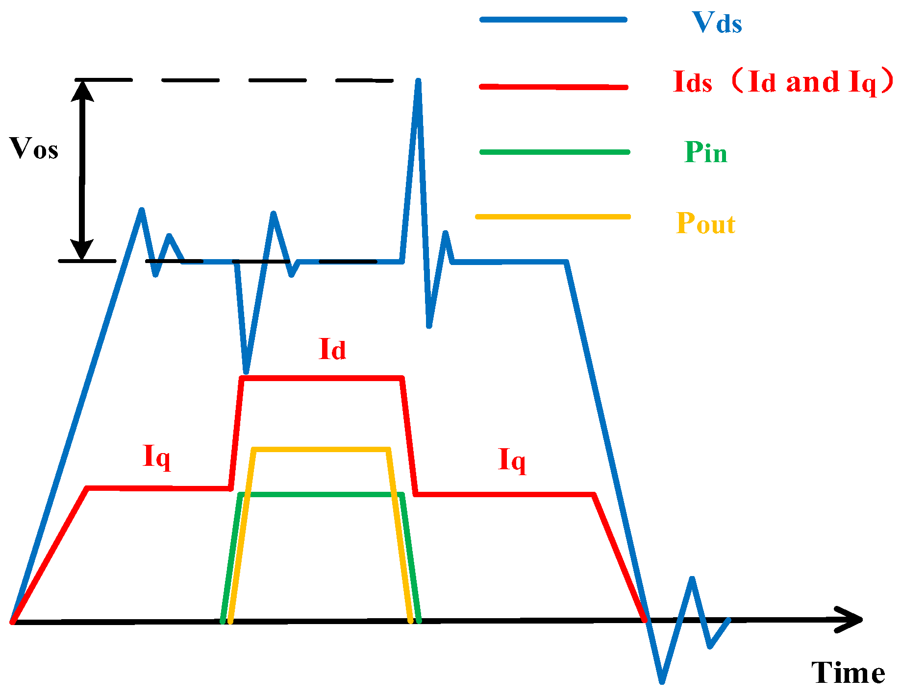
8], as illustrated in
Figure 1, the drain of the power amplifier will have a significant voltage overshoot, which might damage the device due to the sharp rising/falling edges of the pulse. This issue becomes worse with an increased output power.
Vds represents the drain voltage of the pulsed power amplifier, Δt represents the change time, Ids represents the drain current of the pulsed power amplifier, Iq represents the static current, Id represents the dynamic current, Pin represents the input power, and Pout represents the output power.
When the input power is turned off, the drain current changes rapidly from
Id to
Iq, and the voltage overshoot
Vos at the drain of the power amplifier may be described as:
(1) suggests that the sharp drain-current change and the parasitic inductance of the circuit
L determine the voltage overshoot amplitude [
4,
9]. For high-power amplifiers, the difference between
Id and
Iq may be tens of amperes, and Δ
t may only be tens of nanoseconds, so a small inductance
L can cause a large voltage overshoot.
Some literatures solve the problem of voltage overshoot by reducing the current variation or adopting grid modulation, but this will lead to problems of efficiency reduction and waveform deterioration [
7,
10,
11]. This paper solves the problem of voltage overshoot by reducing the parasitic inductance of the circuit.
A significant source of parasitic inductance of the circuit is the parasitic inductance of the bias circuit. The parasitic inductance of the circuit must be reduced to limit voltage overshoot. This research proposes a bias circuit with a lower parasitic inductance that is appropriate for high-power pulsed power amplifiers, since the bias circuit is an important source of parasitic inductance. The proposed bias circuit is also appropriate for the wideband power amplifier due to its broadband characteristics.
2. Analysis and Simulation
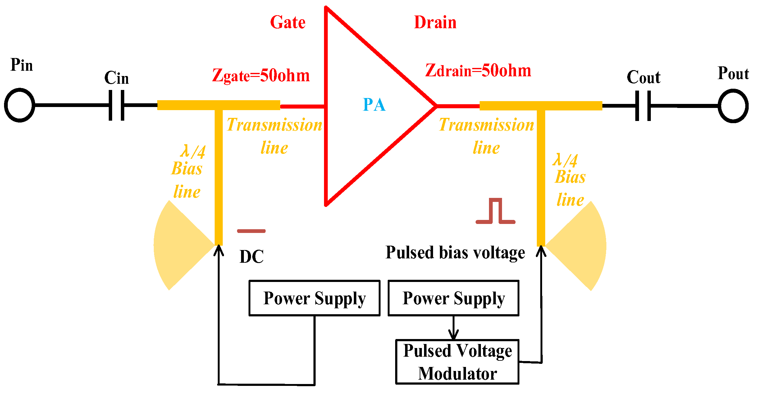
High-frequency power amplifiers typically employ distributed circuits to construct bias circuits, since the parasitic characteristics of discrete components are significant, and the size of distributed circuits is suitable for high-frequency applications. The connection between the power amplifier, the conventional bias circuit, and the power supply is illustrated in
Figure 2. The gate voltage is negative and continuous.
The input and output impedances of the power amplifier are both 50 Ω. Additionally, the input and output ports also have a 50 Ω impedance. Input and output ports are kept separate from the power source using
Cin and
Cout. The power amplifier or the load receives the microwave through the transmission line. In bias lines with radial stubs at one end, microstrip lines with a length of λ/4 are employed [
12]. Impedances that are perceived by the device at the drain side in this configuration are open to odd harmonious frequencies and short to even harmonious frequencies [
13]. As a result, the bias circuit allows the power supply to deliver a DC or pulsed voltage to the power amplifier without transmitting microwave signals to the power supply.
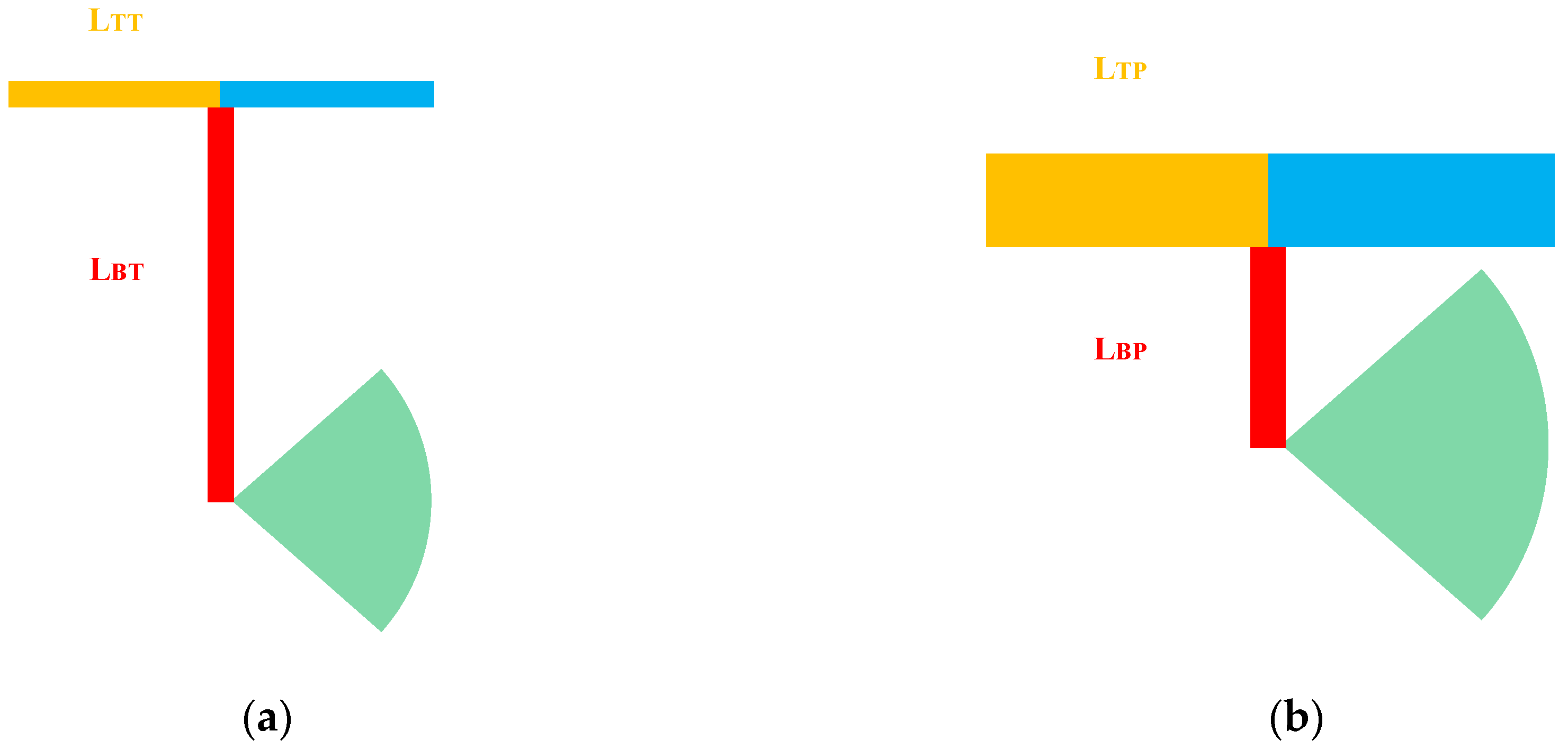
The parasitic inductance of the conventional bias circuit is illustrated in
Figure 3a. The parasitic inductance is the combination of the bias line and a portion of the transmission line. By reducing the bias line’s length and increasing the transmission line’s width, the proposed bias circuit can decrease the bias circuit’s parasitic inductance, as illustrated in
Figure 3b.
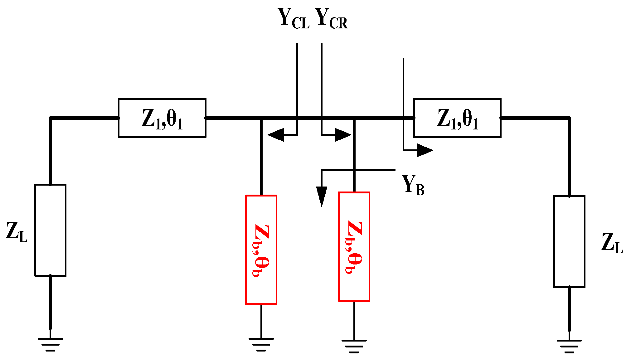
Assume that the proposed bias circuit is symmetric and that the microwave’s ideal short-circuit location is the radial stub. The impedance transformation relation of the proposed bias circuit is shown in
Figure 4. The load
ZL has a 50 Ω impedance.
Z1 is the transmission line’s characteristic impedance,
Zb is twice that of the bias line’s characteristic impedance,
θb is the bias line’s electrical length, and
θ1 is the transmission line’s electrical length.
According to the transmission line impedance formula and transmission line transformation formula, the following equation can be obtained:
Due to the symmetry of the bias circuit, the following equation can be obtained:
In order to satisfy the impedance matching,
YCL and
YCR should be conjugate-matched, and the following equation can be obtained:
The following equation can be obtained by combining (2)–(5):
Assuming that
Z1 is known, tan
θ1 has real solutions when one of the following criteria is met:
According to (7), the following equations can be obtained:
When
Z1 satisfies the criteria mentioned above, the
θ1 can be calculated as:
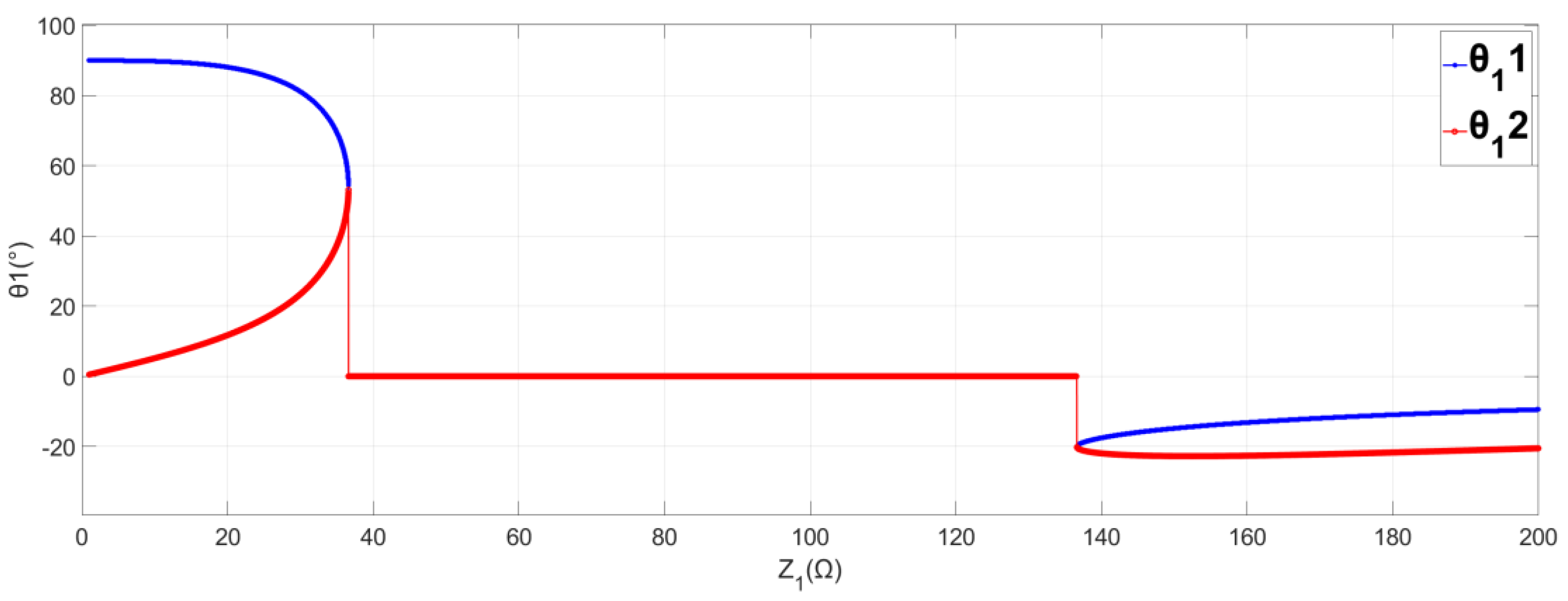
Figure 5 illustrates the relationship between
Z1 and
θ1 when
Zb is set to 200 Ω and
θb to 30°.
Figure 5 shows that
θ11 and
θ12 are positive when
Z1 is less than 36.6 Ω and negative when
Z1 is more than 136.6 Ω. Thus, (7) is required for
θ1 to have at least one solution, as it only makes physical sense if
θ11 and
θ12 are positive. Furthermore, the shorter
θ12 should be employed to minimize the transmission line’s parasitic inductance.
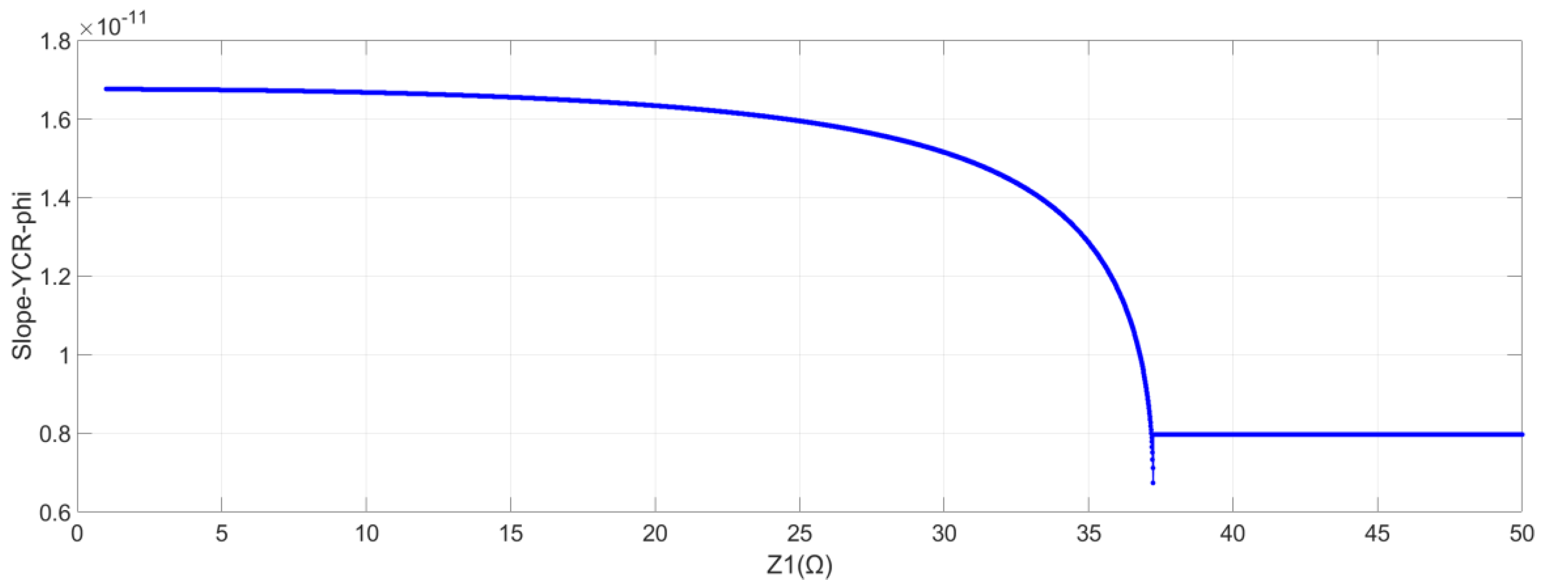
It is discovered that the bias circuit’s bandwidth and the phase of admittance
YCR’s frequency-dependent slope have a negative correlation [
14].
Figure 5 illustrates the relationship between the phase of admittance
YCR’s frequency-dependent slope and
Z1.
Figure 6 demonstrates that when
Z1 satisfies (12), the phase of admittance
YCR’s frequency-dependent slope has a minimum, and the bias circuit’s bandwidth is the largest.
θ11 is equal to
θ12 in this condition.
The 8.5 GHz center frequency is established. For the proposed bias circuit, Zb was set to 200 Ω and θb to 30°, after which the initial values of Z1 and θ1 were set to 36.6 Ω and 53.1°, respectively, according to (11) and (12). For the traditional bias circuit, Zb was set to 200 Ω and θb to 90°, and Z1 and θ1 were set to 50 Ω and 53.1°. The traditional and proposed bias circuits are optimized and simulated by ADS (Advanced Design Software). The simulation of the circuits was performed on a Rogers5880 substrate with a relative dielectric constant of 2.2, a thickness of 0.508 mm, and a metal layer thickness of 35 μm.
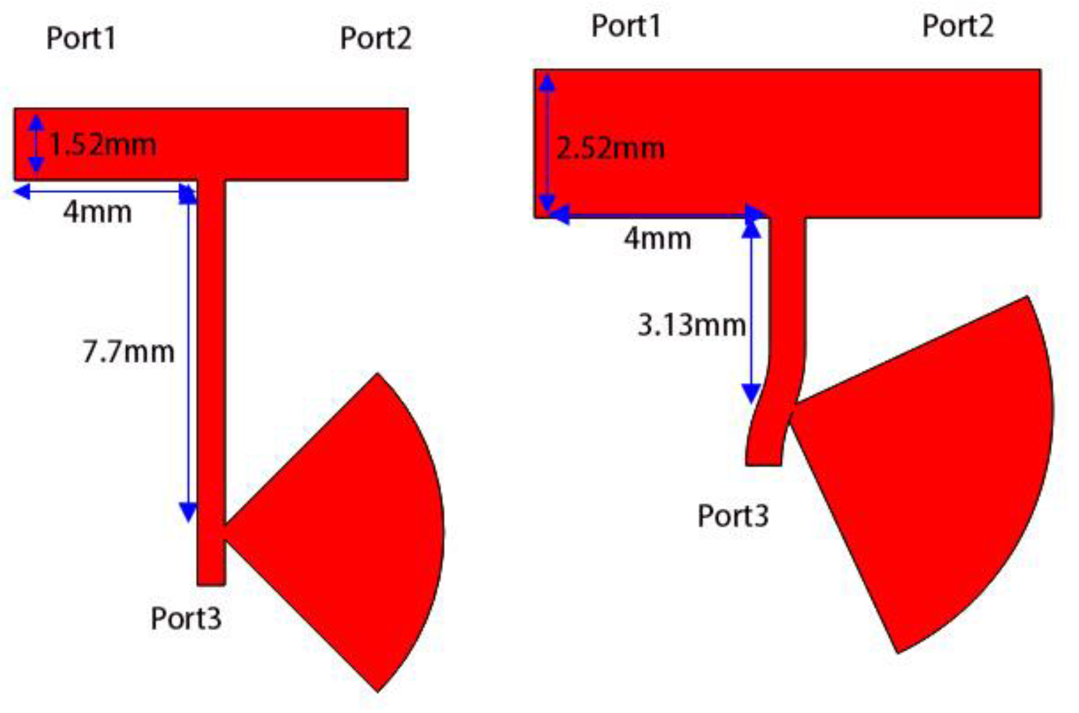
The layout of the traditional bias circuit and the proposed bias circuit are shown in
Figure 7 with the assistance of the software optimization tool.
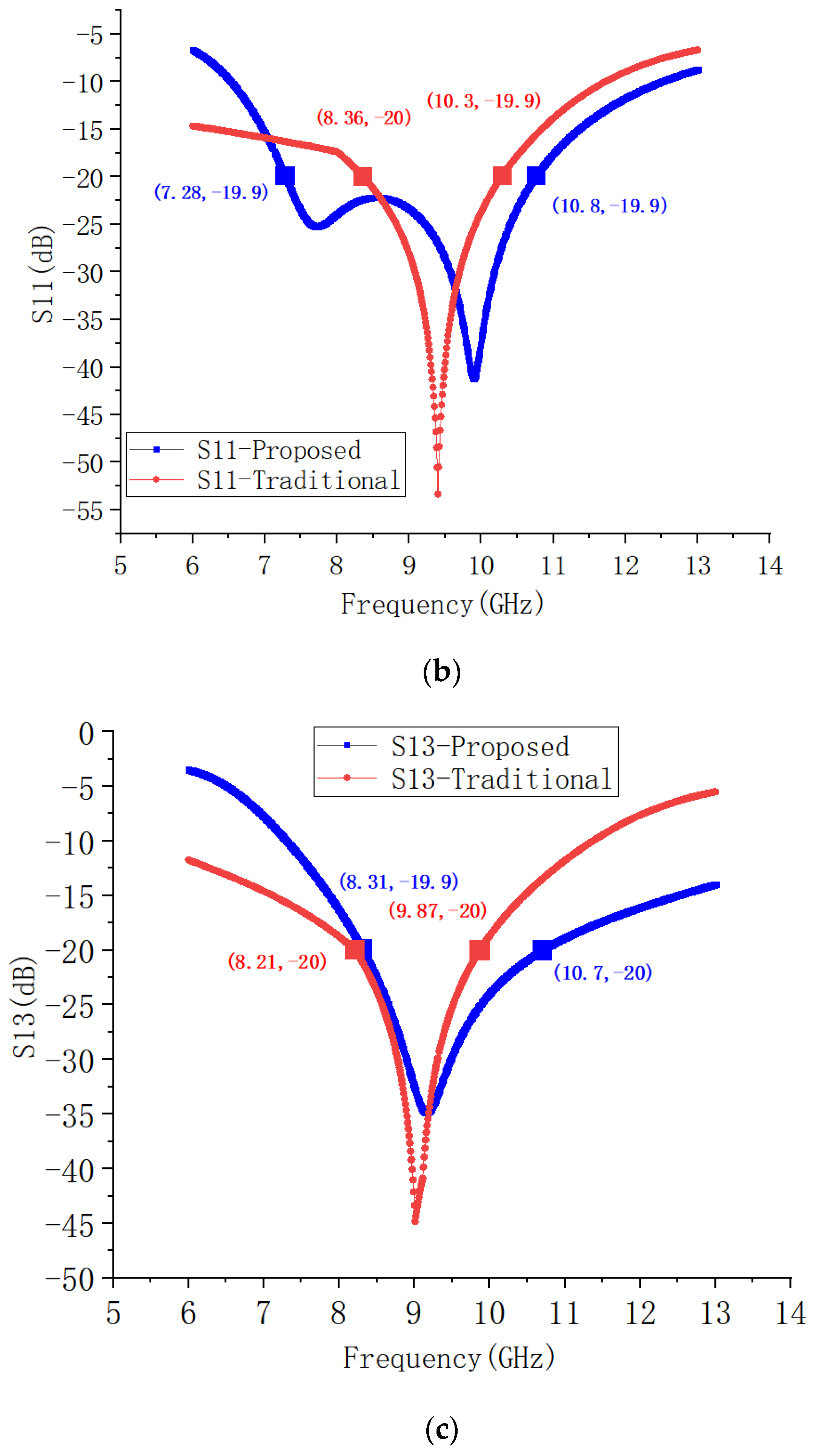
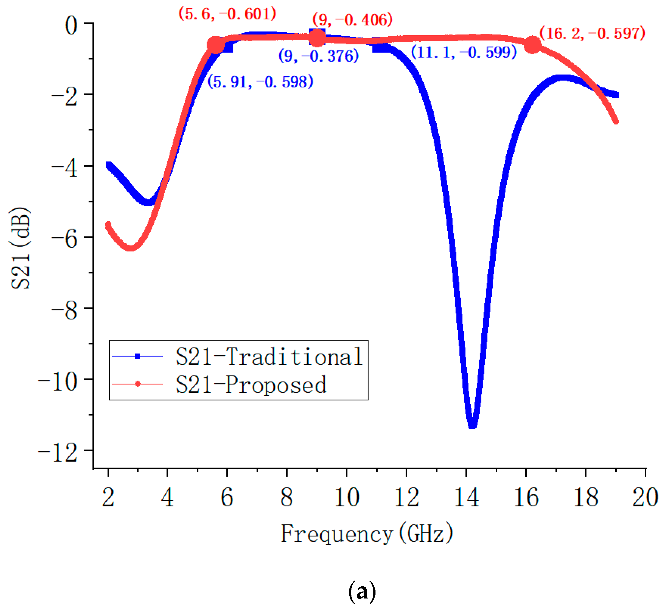
The results of the EM simulation for the S parameters of the proposed bias circuit and the traditional bias circuit are shown in
Figure 8.
Figure 8a is the transmission loss,
Figure 8b is the reflection coefficient,
Figure 8a is the isolation. The simulated return loss of port1 of the traditional bias circuit is less than −20 dB from 8.36 to 10.3 GHz, while the simulated return loss of port1 of the proposed bias circuit is less than −20 dB from 7.28 to 10.8 GHz. According to the simulation results, the proposed bias circuit’s bandwidth is broader than that of the traditional bias circuit.
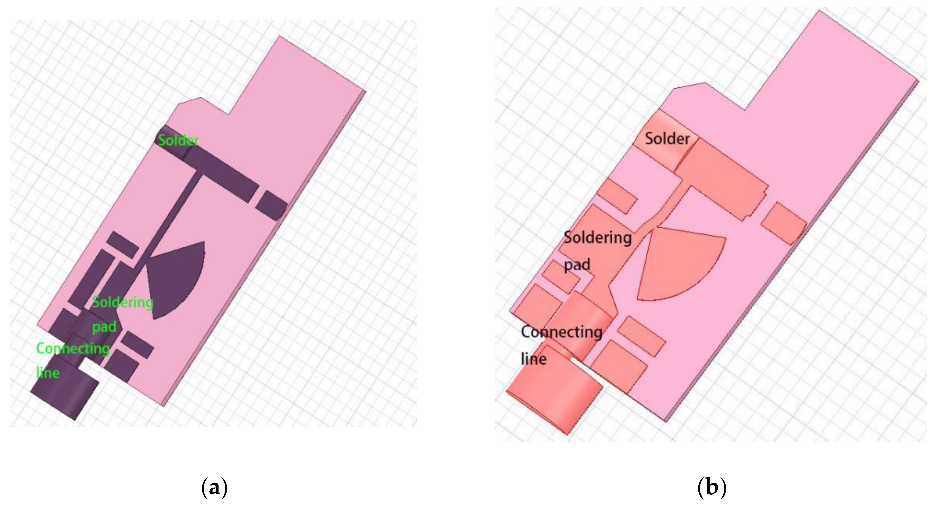
The parasitic inductance of the traditional bias circuit and the proposed bias circuit is simulated by ANSYS. The simulation’s structural diagram is presented in
Figure 9. Besides the bias circuit, the soldering pad of the stability circuit, the solder, and the connecting line between the bias circuit and the modulated power-supply circuit are also included to make the simulation results as realistic as possible.
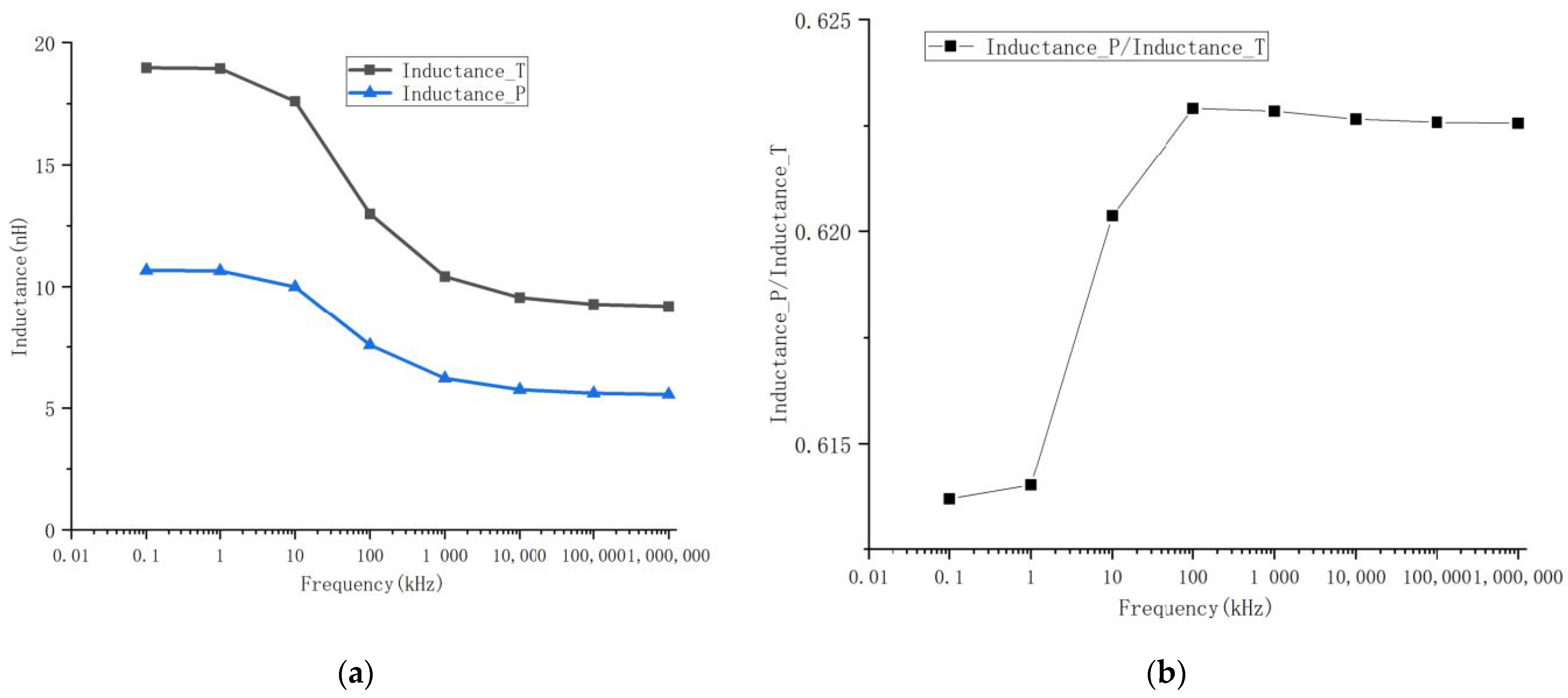
The parasitic inductance of the proposed and traditional bias circuits is illustrated in
Figure 10a varying with frequency.
Figure 10b illustrates the ratio of the parasitic inductance of the proposed bias circuit to that of the traditional bias circuit as a function of frequency. The abscissa of
Figure 10a,b is logarithmic. The parasitic inductance of the proposed bias circuit is about 62% of that of the traditional bias circuit.
3. Experiment and Results
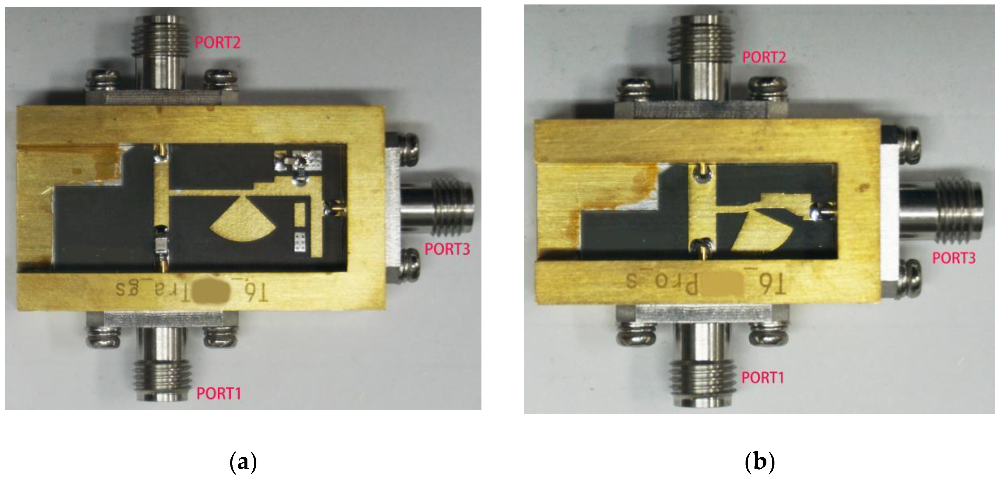
This section fabricated a proposed bias circuit and a traditional bias circuit to validate the proposed method. The layouts of the traditional bias circuit and the proposed bias circuit are shown in
Figure 7. The circuits have been designed and implemented on a Rogers5880 substrate with a relative dielectric constant of 2.2, a thickness of 0.508 mm, and a metal layer thickness of 35 μm. As illustrated in
Figure 11, the fabricated microstrip circuit was welded on the copper base, and the conversion between the microstrip and coaxial part was realized with the SMA joint.
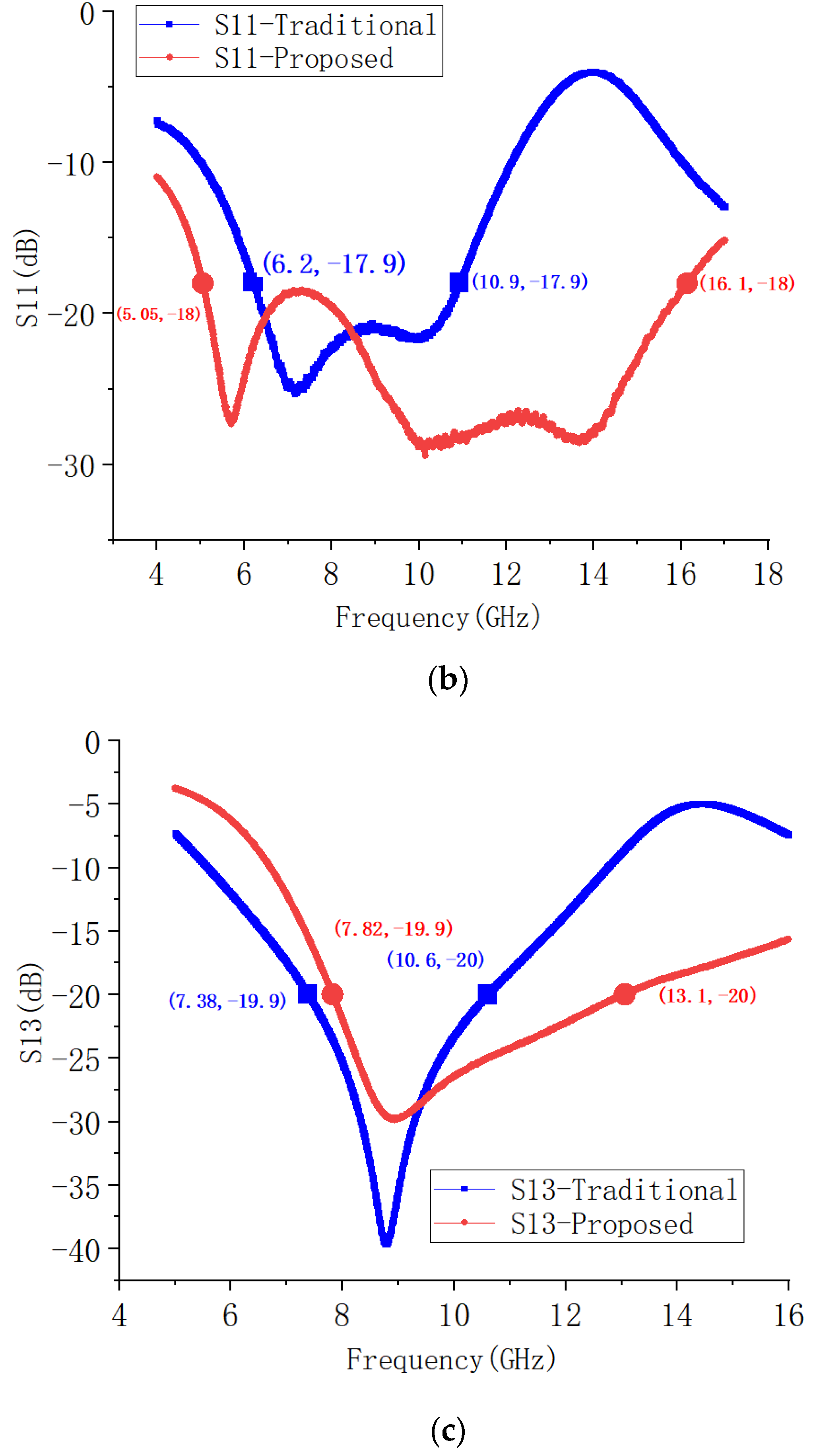
A vector network analyzer was used to measure the S parameters of the traditional bias circuit and the proposed bias circuit. The results of the measurement are shown in
Figure 12. The measured return loss of port1 of the traditional bias circuit is less than −18 dB from 6.2 to 10.9 GHz, while the measured return loss of port1 of the proposed bias circuit is less than −18 dB from 5.05 to 16.1 GHz. According to the measurement results, the proposed bias circuit’s bandwidth is broader than that of the traditional bias circuit.
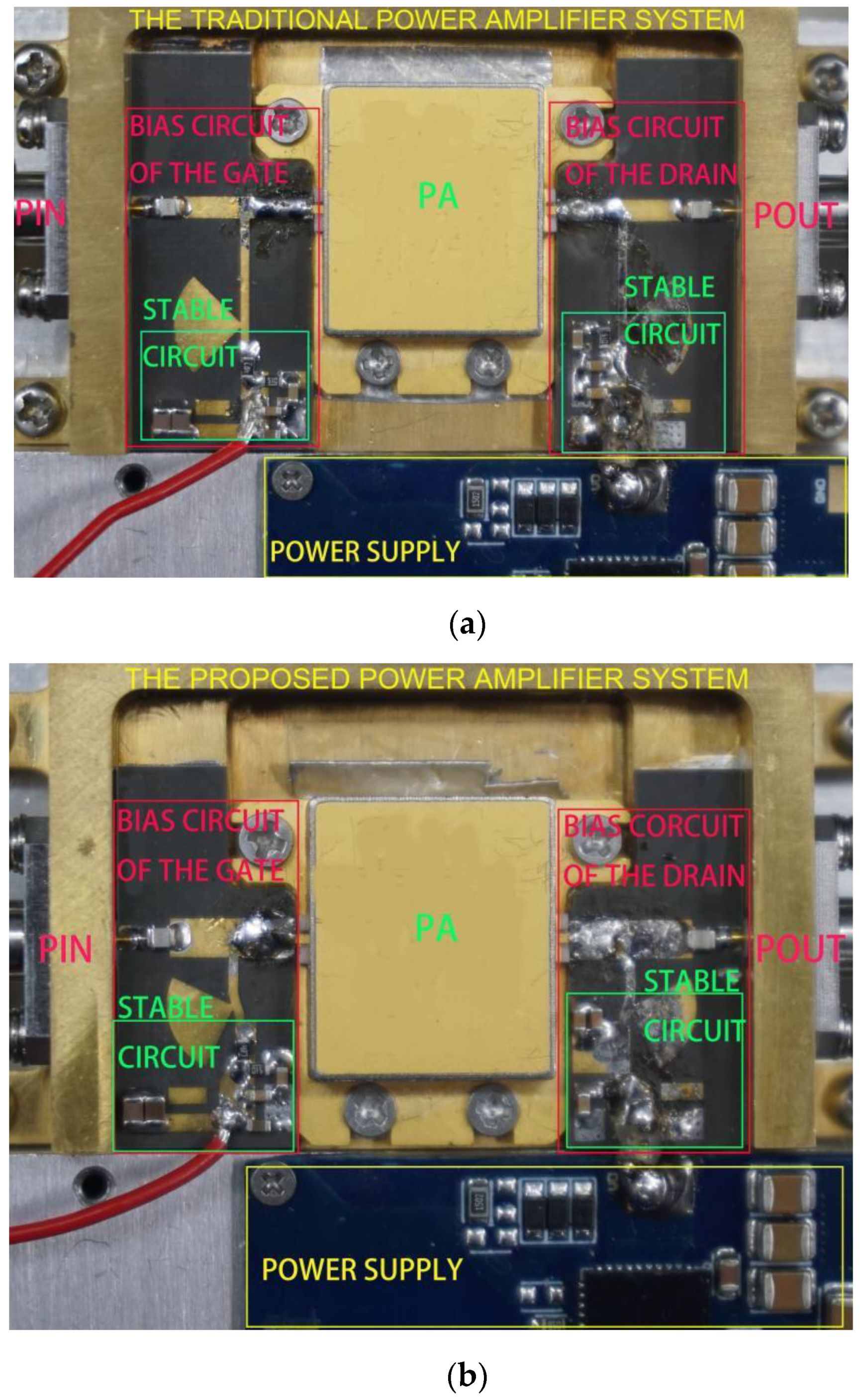
As shown in
Figure 13, the gate bias circuit, the drain bias circuit, and the power amplifier are fixed on the same metal base to form a power-amplifier system. The bias circuit is secured by welding. The power amplifier is secured by screws, and a layer of indium foil with a thickness of 0.1 mm is placed underneath the power amplifier to improve heat dissipation and grounding. The gate bias circuit has the same fundamental components as the drain bias circuit, such as the bias line and a portion of the transmission line. In fact, the gate bias circuit has a different stable circuit from the drain bias circuit, but the S parameter is unaffected. The power-amplifier system composed of the traditional bias circuit is called the traditional power-amplifier system, and the power-amplifier system composed of the proposed bias network is called the proposed power-amplifier system.
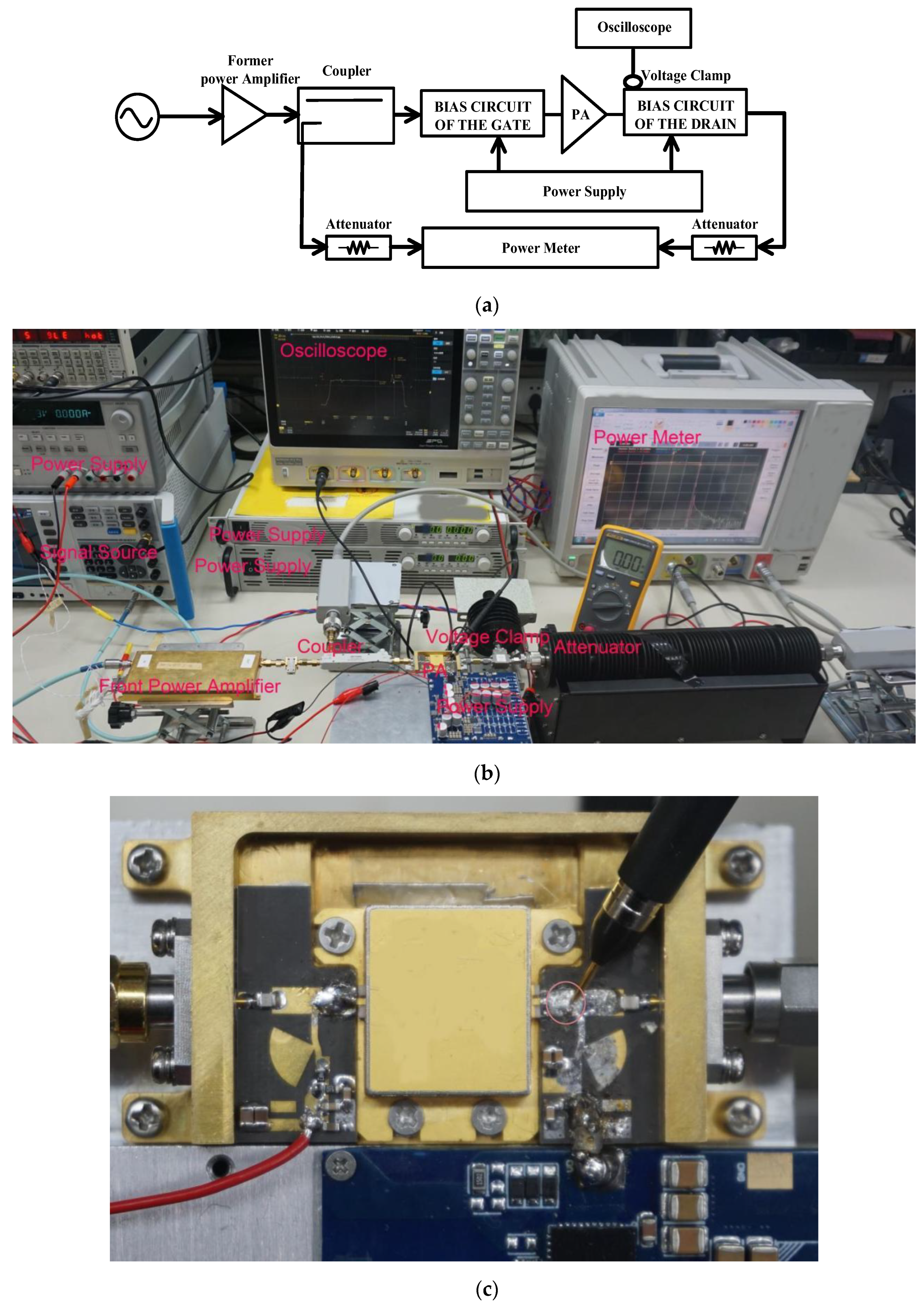
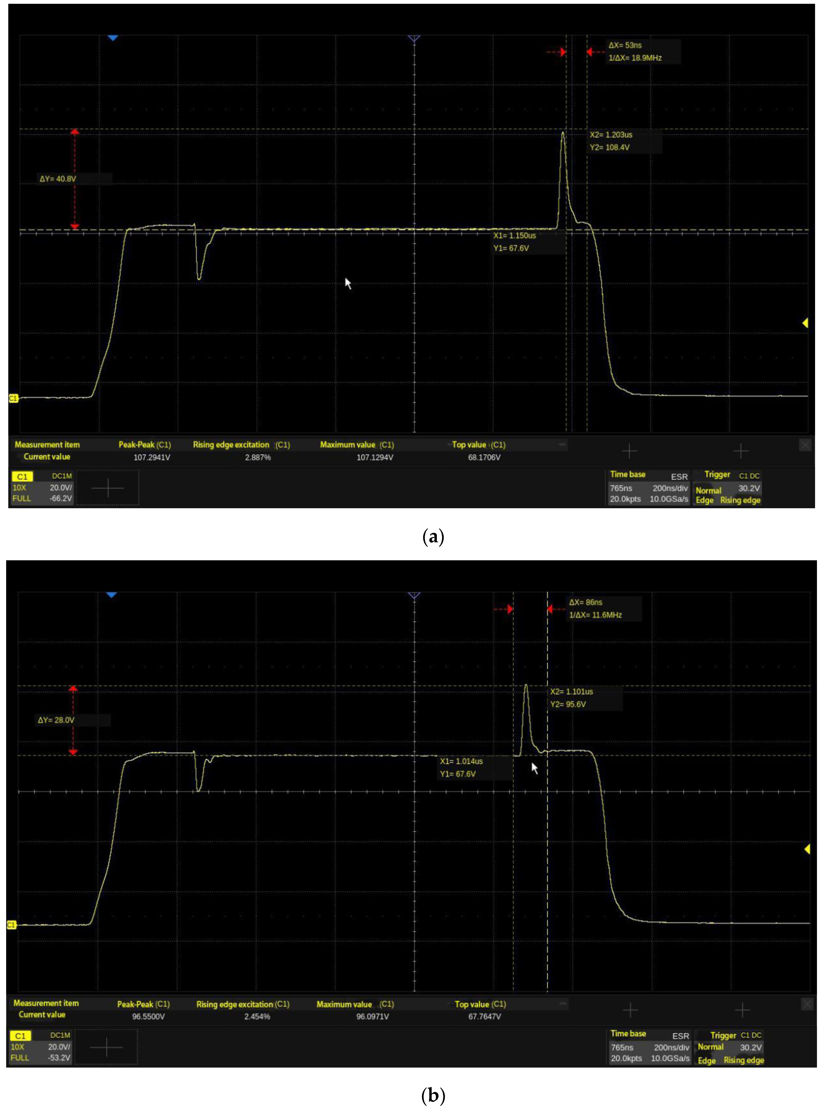
A measurement system is built to measure the voltage overshoot of the traditional power-amplifier system and the proposed power-amplifier system. The schematic diagram of the measurement system is shown in
Figure 14a, and its physical diagram is shown in
Figure 14b. The signal source controls the frequency and power of the microwave. The front power amplifier generates the driving signal. The oscilloscope and the voltage probe jointly measure the voltage waveform of the bias circuit. The power meter detects the power of the driving signal as well as the output power of the power-amplifier system. The voltage probe measurement location, where the power amplifier connects to the bias circuit, is illustrated in detail in
Figure 14c. The voltage probe has no impact on the power-amplifier system, since its impedance is greater than 10 MΩ.
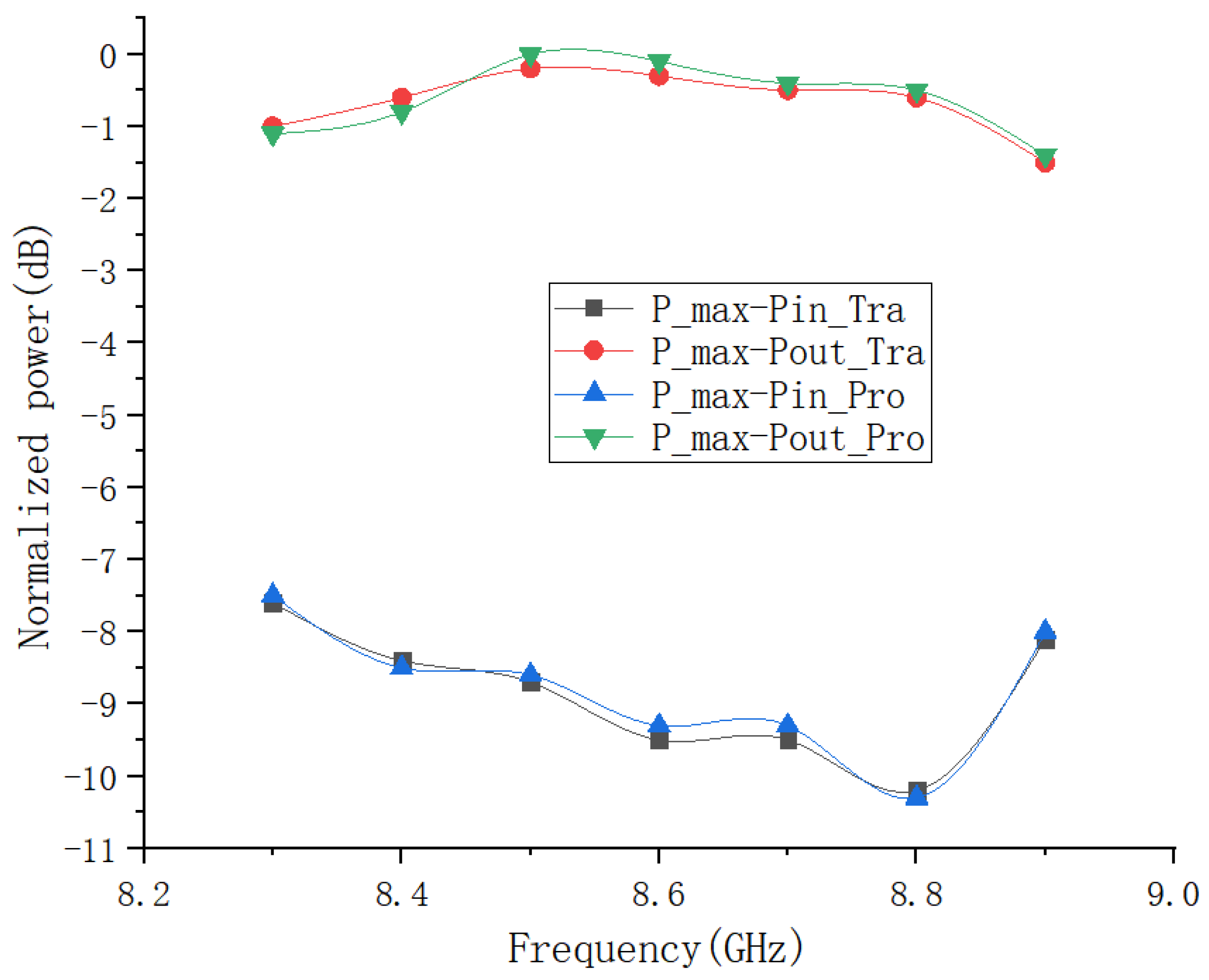
Both the traditional and proposed power-amplifier systems operate in class AB mode. The gate voltage of traditional and proposed power-amplifier systems is fixed at −1.8 V. The input and output power of the traditional and proposed power-amplifier systems was set to be basically the same. As shown in
Figure 15, the input and output powers of the traditional and proposed power-amplifier systems are normalized to the difference from the maximum power P_max, which is the kW level.
The drain voltage of the traditional power-amplifier system and the proposed power-amplifier system was also set to the same 67.6 V, so the static drain current of the traditional power-amplifier system is the same as the static drain current of the proposed power-amplifier system. Because the output power is the product of the drain voltage and the dynamic drain current, the drain current of the traditional power-amplifier system is the same as that of the proposed power-amplifier system. According to (7), the drain voltage of the power-amplifier system Vds is proportional to the parasitic inductance of the bias circuit L, assuming that the static drain current Iq and the dynamic drain current Id are constant. Therefore, the ratio of the parasitic inductance of the traditional power-amplifier system to that of the proposed power-amplifier system is equal to the ratio of the voltage overshoot of the traditional power-amplifier system to that of the proposed power-amplifier system.
Figure 16 shows the measured voltage waveform of the bias circuit of the traditional power-amplifier system and the proposed power-amplifier system. The voltage overshoot of the traditional power-amplifier system is 28 V, while the voltage overshoot of the proposed power-amplifier system is 40.8 V. The ratio of the voltage overshoot of the traditional power-amplifier system to that of the proposed power-amplifier system is 0.686. Thus, the ratio of the parasitic inductance of the traditional power-amplifier system to that of the proposed power-amplifier system is 0.686.
The measurement ratio is slightly larger than the simulation ratio, because the connection wire and solder in the simulation model are not the same as the actual connection line and solder.
4. Conclusions
The power amplifier’s drain will suffer a voltage overshoot caused by the pulse’s rapid rising/falling edges. Since the difference between the static and dynamic current is small for low-power amplifiers, the voltage overshoot’s magnitude may be disregarded. A small inductance, however, can result in a significant voltage overshoot in high-power amplifiers, since the difference between the static and dynamic current can be tens of amperes. Additionally, the voltage overshoot increases in proportion to the circuit’s parasitic inductance. The parasitic inductance of the bias circuit contributes to the voltage overshoot’s magnitude. By reducing the bias line’s length and increasing the transmission line’s width, the proposed bias network in this article can reduce the parasitic inductance of the bias network. The proposed bias circuit’s parameters can be obtained using impedance matching. The bandwidth of the proposed bias circuit is better than those of the traditional bias circuit, based on the layout simulation results in simulation software. Meanwhile, according to simulation results, the proposed bias circuit’s parasitic inductance is about 2/3 of that of the traditional bias circuit. The measurement results of the S parameters of the traditional and proposed bias circuit prove that the proposed bias circuit’s bandwidth is broader than that of the traditional bias circuit. In addition, the measured ratio of the parasitic inductance of the traditional power-amplifier system to that of the proposed power-amplifier system is 0.686, which is slightly higher than the simulated ratio. In summary, on the premise of satisfying the basic characteristics of the biasing circuit, the proposed bias circuit is more suitable for high-power pulsed power amplifiers, since it has a broader bandwidth and lower parasitic inductance.

 ,
, 


