Article

Analysis and Design of a Dual-Frequency Capacitive Power Transfer System to Reduce Coupler Voltage Stress

1
Tangshan Graduate School, Southwest Jiaotong University, Tangshan 063000, China
2
School of Electrical Engineering, Southwest Jiaotong University, Chengdu 611756, China
3
Qingdao Metro Operation Co., Ltd., Qingdao 266000, China
*
Author to whom correspondence should be addressed.
Electronics 2023, 12(6), 1274; https://doi.org/10.3390/electronics12061274
Submission received: 18 January 2023 / Revised: 22 February 2023 / Accepted: 28 February 2023 / Published: 7 March 2023

Abstract

:
In a capacitive power transfer (CPT) system, the coupling capacitance formed between the coupling plates is very small only in the pF or nF range, which leads to high voltage stress among the coupling plates during energy transmission, which increases the risk of an electrical breakdown between the coupled plates. To solve this problem, a novel dual-frequency CPT system is proposed in this paper, which uses the “peak clipping” effect caused by the superposition of the fundamental wave and third harmonic wave to reduce the voltage stress of the coupled plates. Through the detailed analysis of the working principle of the CPT system, it is shown that the dual-frequency CPT system can indeed reduce the high voltage stress among the coupled plate to 84.3% of the equivalent single-frequency system and can also reduce the inverter conduction losses to 90%. A 200 W prototype is designed with the proposed scheme, and the experimental results confirm the correctness of the theoretical derivation.

1. Introduction

As a new non-contact power supply technology, wireless power transfer (WPT) technology removes the shackle of power lines and greatly improves the flexibility of power supply equipment. Meanwhile, this technology can avoid the potential safety problems while charging caused by traditional contact charging, since it has no contact sparks and is not affected by rain, snow, or other harsh environmental factors [1]. WPT technology is widely used because of its power supply safety, flexibility, and reliability [2,3,4,5,6]. At present, the transmission modes of WPT are mainly divided into inductive power transfer (IPT) and capacitive power transfer (CPT). An IPT system uses a high-frequency magnetic field generated by coupling coils for power transmission, while CPT technology uses a high-frequency electric field generated by coupling plates for power transmission [7,8]. IPT has been proposed for many years and has made good achievements in the field of WPT, with transmission power up to 1 MW [9], and system optimization can increase the efficiency to 96% [10]. However, an IPT system requires the use of a large number of magnetic cores and expensive Litz wires to construct a high-frequency magnetic field as a medium for power transmission, resulting in a high cost and the heavy coupling mechanism of the IPT system. In addition, the high-frequency magnetic field will cause eddy current loss in the surrounding metals, which increases the power loss of the system and reduces the efficiency of the system [11]. Moreover, magnetic field radiation also poses a threat to the personal safety of organisms [12]. In contrast, a CPT system uses a high-frequency electric field to transmit power without magnetic field radiation, so it can be applied to the wireless charging of implantable biomedical devices. A CPT system is proposed that uses a displacement current to realize the wireless charging of the subcutaneous sensors in [13]. With the human tissue layer as the transmission medium, the corresponding CPT system’s coupling mechanism model is established, which realizes the research and development of a wireless power supply system suitable for the human implantable medical devices in [14,15,16]. In addition, the CPT system uses lower-cost and lighter-weight aluminum plates as the coupling mechanism, so it is suitable for electric locomotive charging, with its strict cost and weight restrictions. Refs. [17,18,19] show that a lot of research has been accomplished on the coupling mechanism model and compensation topology of the static-charging CPT systems of electric vehicles. In [20], the coupling capacitance is formed by transforming the tire and the ground to realize a dynamic wireless power supply for electric vehicles. Ref. [21] proposes a coupling mechanism model suitable for rail transit, which can provide electric energy for moving locomotives. In addition, a CPT system is not sensitive to metals and has good environmental compatibility. In [22], a wireless power supply for refrigerated containers made of metal is realized. In [23], a CPT system is proposed for the internal winding of a motor. Therefore, CPT has been widely studies by scholars in China and around the globe because of its lower cost, better environmental compatibility, and negligible eddy current loss.
However, CPT systems usually have very high voltage stresses between their coupled plates due to the very small coupling capacitance that is only in the pF or nF range. The high voltage at both ends of the coupled plate lead to the emission of a strong electric field and even the risk of dielectric breakdown [10]. Therefore, reducing the voltage stress on the coupled plate is a key problem. The voltage on the coupling plate can be reduced by increasing the switching frequency of the inverter (that is, adopting a larger system frequency), but the system efficiency is reduced due to the increase in switching loss [24], and the higher frequency requires the higher performance of the device itself. In addition, in [25], the coupling voltage stress can also be reduced by increasing the coupling capacitance formed between the coupling plates. However, in some specific scenarios, due to the limitations of the external environment, the capacitance value formed by the coupling plates has already been determined, or it is difficult to increase the rating value required by the system. In [21], the voltage on both sides of the coupling plate is changed by adjusting the resonant network and the isolation transformer to reduce the voltage between the coupling plates. Ref. [10] proposes a parameter design method for a two-sided LCLC compensation CPT system based on the pre-designed voltage limit of the coupled plate. Ref. [26] redistributes the voltage stress on all the compensation components and coupling plates through a mathematical calculation based on a double-sided LC compensation circuit and reduces the voltage stress of the coupling plate by optimizing the compensation network and system parameters in a single-frequency system.
In this paper, a novel voltage stress optimization approach is proposed to reduce the voltage stress of the coupled plate by introducing the voltage component of the third harmonic frequency. As shown in Figure 1, the superposition of the primary and tertiary frequency voltages can produce an obvious “peak clipping” effect. A multi-frequency system has been studied for IPT. Ref. [27] makes a detailed performance analysis of a multi-frequency power transmission system for IPT. Refs. [28,29,30] realizes multi-channel and multi-load energy transmission by using a multi-frequency IPT system. However, compared with IPT, CPT has a different coupling structure and compensation topology, so the analysis of a multi-frequency power transmission system in an IPT system cannot be directly applied to a CPT system.
In this paper, a new dual-frequency CPT system is proposed. Due to its special compensation network design, both the primary and tertiary frequency voltage components of the inverter output voltage can be utilized to transmit energy at two frequencies. In addition, the voltage stress of the coupling plate can be reduced by controlling the ratio of the transmitted energy of the two frequencies, while the conduction loss of the inverter can be reduced. The contributions of this paper are as follows. (a) A CPT system capable of dual-frequency power transmission is proposed. Compared with the equivalent single-frequency system, a dual-frequency system can reduce the voltage stress amplitude on the coupled plate and also reduce the conduction loss of the inverter. (b) The working principle of the dual-frequency CPT system is analyzed in detail, and the control strategy of the energy transmission ratio between the primary and tertiary frequency channels is proposed. (c) According to the theoretical derivation scheme, a test prototype is designed to verify the correctness of the proposed theory.
The rest of this paper is organized as follows. In the Section 2, the proposed circuit model is introduced systematically, including the dual-power equivalent model and the resonant unit module equivalent model. Then, the circuit analysis of the proposed dual-frequency system is carried out to obtain the control method of the power transmission ratio at different frequencies. In the Section 3, the equivalent fundamental single-frequency circuit is introduced, and the single-frequency circuit and the dual-frequency circuit are compared and analyzed. The influence of the introduction of the third harmonic frequency voltage component on the voltage stress among the coupled plates and the inverter conduction losses is explained in detail. Then, the system parameter design process is given. In Section 4, the correctness of the proposed theory is verified by simulation and experiment. The Section 5 summarizes the full text.

2. System Description and Working Principle

2.1. System Description

The dual-frequency CPT system is shown in Figure 2a. The system has two power sources that provide power at two frequencies from the fundamental and third harmonic frequency voltage components of the full-bridge inverter output voltage. Assuming that the duty ratio of the full-bridge inverter is 50%, the rectangular wave voltage v i n t on the AC side can be decomposed into a Fourier series composed of odd harmonics.
v i n t = 4 V d c π n = 1 sin 2 n 1 ω t 2 n 1 ,         n = 1 , 2 , 3 ,
For different frequencies, we can define each parameter separately and express it with corresponding subscripts (i.e., 1 represents the fundamental wave, and 3 represents the third harmonic wave). The root mean square value of the fundamental and third harmonic voltage can be expressed as
V i n , 1 = 2 2 V d c π ,     V i n , 3 = 2 2 V d c 3 π
The resonant compensation structure adopts a topological structure similar to that of a double-sided LC, though different from the general double-sided LC compensation. Due to the need to make the system reach the resonant condition at the same time under the dual frequencies of the fundamental and third harmonic, we need to specifically design the resonant compensation module. In Figure 2b, the original single impedance element is replaced by a combination of L i and C i connected in parallel in series C i (or L j and C j connected in parallel in series L j ) [30], so the equivalent impedance is represented by Z i or Z j ; then,
Z i = j ω L i 1 ω 2 L i C i + 1 j ω C i       i = 1 , 4 Z j = j ω L j 1 ω 2 L j C j + j ω L j       j = 2 , 3
The two capacitors formed by the coupled plates are a series structure. The equivalent capacitance can be represented by C X , and the equivalent impedance can be represented by Z X , namely,
C X = C m 2 ,     Z X = 1 j ω C X = 2 j ω C m
The equivalent Π-type circuit model of the dual-frequency CPT system is shown in Figure 2c. The full-bridge inverter generates high-frequency AC voltage to supply power to the primary side resonant network. The high voltage of the fundamental and third harmonic frequency voltages, V i n , 1 and V i n , 3 , respectively, raised by the resonant network generates a displacement current between the coupling plate and then supplies power to the load end after the secondary resonant network depressurizes. The key condition for the normal operation of the dual-frequency system is that the input impedance of the system is very low at both frequencies to realize the dual-frequency wireless power transmission.

2.2. Working Principle

Figure 2d shows the equivalent T-type circuit model transformed from the Π-type circuit model of the dual-frequency CPT system. So
Z 2 X = Z 2 Z X Z 2 + Z 3 + Z X , Z 3 X = Z 3 Z X Z 2 + Z 3 + Z X ,   Z 23 = Z 2 Z 3 Z 2 + Z 3 + Z X
The relation between the input current I i n , output current I o u t , and input voltage V i n can be expressed as
V i n 0 = Z 1 + Z 2 X + Z 23 Z 23 Z 23 Z 23 + Z 3 X + Z 4 + R L · I i n I o u t
In order to achieve the resonant state of the system to achieve the zero phase angle (ZPA) characteristic,
Z 1 + Z 2 X + Z 23 = 0 ,           Z 23 + Z 3 X + Z 4 = 0
According to Equations (6) and (7), I i n and I o u t can be expressed as
I i n = V i n R L Z 23 2 ,     I o u t = V i n Z 23  
According to Formula (6), Z 23 determines the values of the input current I i n and output current I o u t when V i n and R L are constant. Therefore, we can control the power transmission ratio at different frequencies by controlling the value of Z 23 at different frequencies.

3. System Design Considering Coupler Voltage Stress and Inverter Conduction Losses

A constant, k , is used to represent the ratio of power transmission at different frequencies. P o u t is the total transmission power; P o u t , 1 and P o u t , 3 represent the transmission power under the fundamental and third harmonic frequencies, respectively.
P o u t , 1 = k P o u t ,   P o u t , 3 = 1 k P o u t
In the ideal state without considering the system loss, the transmission power of the system can be expressed as
P o u t , 1 = I o u t , 1 2 R L = V i n , 1 Z 23 , 1 2 R L ,             P o u t , 3 = I o u t , 3 2 R L = V i n , 3 Z 23 , 3 2 R L
Here, we assume an equivalent fundamental single-frequency system that transmits the same amount of power as the dual-frequency system. In the following derivation, we define the single-frequency system and the dual-frequency system with the subscripts s and d, respectively, so
P o u t , s = I o u t , s 2 R L = V i n , 1 Z 23 , s 2 R L
By combining Equations (9)–(11), Equation (12) can be obtained.
1 Z 23 , 1 2 = k Z 23 , s 2   ,     1 Z 23 , 3 2 = 9 1 k Z 23 , s 2
We take Z 23 , s as the base value, so the unit values Z 23 , 1 * and Z 23 , 3 * can be expressed as
Z 23 , 1 * = 1 k ,     Z 23 , 3 * = 1 9 1 k

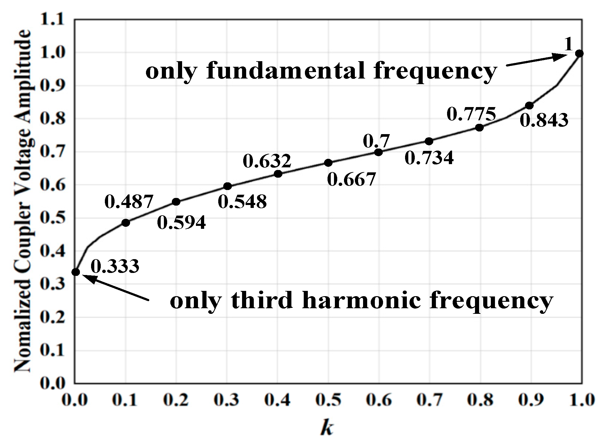
3.1. Analysis of Coupler Voltage Stress

According to Figure 2c, the equations of KVL are
V i n 0 0 = Z 1 + Z 2 Z 2 0 Z 2 Z 2 + Z X + Z 3 Z 3 0 Z 3 Z 2 + Z 4 + R L · I i n I m I o u t
By combining Equations (5), (7), (8) and (14), Equation (15) can be obtained.
I m = V i n Z 2 + Z X + Z 3 R L + Z 3 2 Z 2 Z 3 2
Then, the coupler voltage V m can be represented as
V m = V i n Z m Z 2 + Z X + Z 3 R L + Z 3 2 Z 2 Z 3 2 = V i n Z m Z 2 · 1 + Z 2 + Z X + Z 3 R L Z 3 2
Although dual-frequency power transmission results in the existence of two power transmission “channels” that can themselves be controlled independently by the corresponding parameters at their respective frequencies, the relative positioning of the voltage components at the two frequencies is still very important, especially when considering the voltage stress of the coupled plate. Since the relative positioning between two signals at different frequencies cannot be defined by using the phase shift angle, we select a special position: inverter output terminal voltage v i n t . Here, there is no phase shift when the fundamental and third harmonic voltage components refer to a common origin, namely,
v i n t = 2 V i n , 1 sin ω t + 2 V i n , 3 sin 3 ω t .
As shown in Figure 1, the voltage components v m , 1 t = V m , 1 sin ω t + θ 1 and v m , 3 t = V m , 3 sin 3 ω t + θ 3 of the coupled plate voltage v m t at the two frequencies need to meet the following conditions in order to achieve the desired “peak clipping” effect.
θ 3 3 θ 1 = 2 n π ,       n = 0 , ± 1 , ± 2
When Equation (19) is true, Equation (18) is satisfied.
Z 3 2 Z 2 + Z X + Z 3 R L
Equation (20) can be obtained by simplifying Equation (16).
V m = V i n Z m Z 2
Equation (19) is not difficult to realize, so take one of the cases, Equation (21), to simplify the operation.
Z 23 = Z 2 Z 3 Z 2 + Z X + Z 3 = Z 2
So
Z X + Z 2 + 2 Z 3 = 0
V m = V i n Z m Z 23
It should be noted that Equation (19) should still be met in the subsequent parameter design. With V m , s as the basic value, the normalized value of the fundamental and the third harmonic frequency components ( V m , 1 * and V m , 3 * ) in the plate voltage of the dual-frequency system can be expressed as
V m , 1 * = Z m , 1 * Z 23 , 1 * = k ,     V m , 3 * = Z m , 3 * 3 Z 23 , 3 * = 1 k 3
Then, the voltage v m , d t on the coupled plate of the dual-frequency system can be expressed as
v m , d t = 2 V m , s k sin ω t + 1 k 3 sin 3 ω t
Taking the voltage amplitude V m , s , m a x = 2 V m , s as the basic value, the normalized coupler voltage amplitude V m , d , m a x * of the dual-frequency system can be expressed as
V m , d , m a x * = m a x k sin ω t + 1 k 3 sin 3 ω t
According to Equation (26), the relationship between the normalized coupler voltage amplitude V m , d , m a x * and power-sharing ratio k in the dual-frequency system can be obtained, as shown in Figure 3. The higher the proportion of energy transmitted through the third harmonic frequency “channel” is, the lower the voltage stress among the coupled plates is. When the energy is transmitted only through the third harmonic frequency “channel”, the voltage stress on the coupled plate is 33.3% of the equivalent single-frequency system. This shows that it is viable to reduce the voltage stress among the coupled plates by simultaneously transmitting energy at the fundamental and third harmonic frequencies. Of course, the power-sharing ratio k value should also pay attention to the influence of other factors.

3.2. Analysis of Inverter Conduction Losses

According to Equation (8), the inverter currents of the equivalent single-frequency system and the dual-frequency system can be expressed as
I i n , s = V i n , 1 R L Z 23 , s 2 ,   I i n , 1 = V i n , 1 R L Z 23 , 1 2 ,   I i n , 3 = V i n , 3 R L Z 23 , 3 2
Further, it can be concluded that when compared with the equivalent single-frequency system, the normalized inverter conduction losses P i n l o s s , d * of the dual-frequency system can be expressed as
P i n l o s s , d * = P i n l o s s , d P i n l o s s , s = I i n , 1 2 + I i n , 3 2 I i n , s 2 = k 2 + 9 1 k 2
According to Equation (28), the relationship between the normalized inverter conduction losses P i n l o s s , d * and power-sharing ratio k in the dual-frequency system can be obtained, as shown in Figure 4. When the energy is transmitted only through the third harmonic frequency “channel”, the inverter conduction losses are nine times that of the equivalent single-frequency system. When k = 0.9 , the inverter conduction losses P i n l o s s , d of the dual-frequency system are the smallest: 90% of the equivalent single-frequency system with the same transmission power.

3.3. System Parameter Design

The coupler voltage amplitude V m , d , m a x and inverter conduction losses P i n l o s s , d of the system under different conditions can be obtained, as shown in Table 1. By controlling the power-sharing ratio k = 0.9 , the voltage stress among the coupled plates and inverter conduction losses of the dual-frequency system are better than those of the single-frequency system.
To reduce the voltage stress among the coupled plates, a parameter design method based on the dual-frequency CPT system is proposed as follows.
First, determine the pre-designed system parameters V i n , f , and C m and total output power P L , where C m is directly measured by measuring equipment. Then, the appropriate power-sharing ratio k is selected. In this paper, k = 0.9 is finally selected through the analysis of the system. Second, based on the selected system parameters, the appropriate Z 23   ( Z 23 , 1 and Z 23 , 3 ) is selected according to Equation (13). To obtain the value of each element, we must calculate the different values of each compensation block Z i ( i = 1 ,   4 ) and Z j ( j = 2 ,   3 ) at two frequencies. Based on the existing analytical derivation, Z 2 and Z 3 can be obtained from Equations (21) and (22), respectively. Third, based on the Π-type to T-type transformation relationship, Z 2 X and Z 3 X can be obtained according to Equations (5) and (7), respectively. To realize the load-independent constant current (CC) output and input zero phase angle (ZPA), we can obtain Z 1 and Z 4 according to Equation (7). Finally, based on the different values of Z 1 , Z 2 , Z 3 , and Z 4 at both frequencies, the parameter values of each inductor and capacitor element can be flexibly designed according to Equation (3). The system design process of the proposed dual-frequency CPT system is shown in Figure 5.

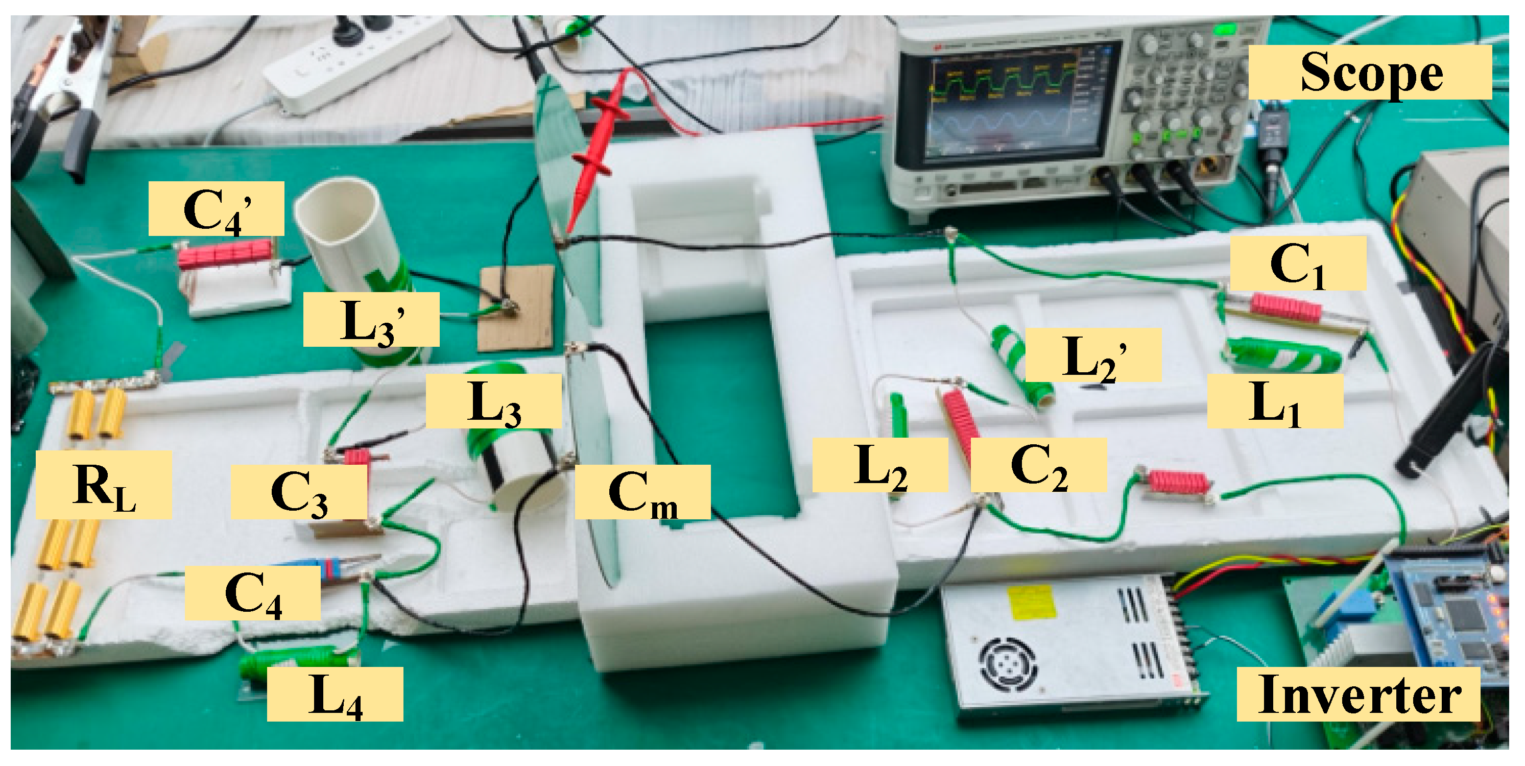
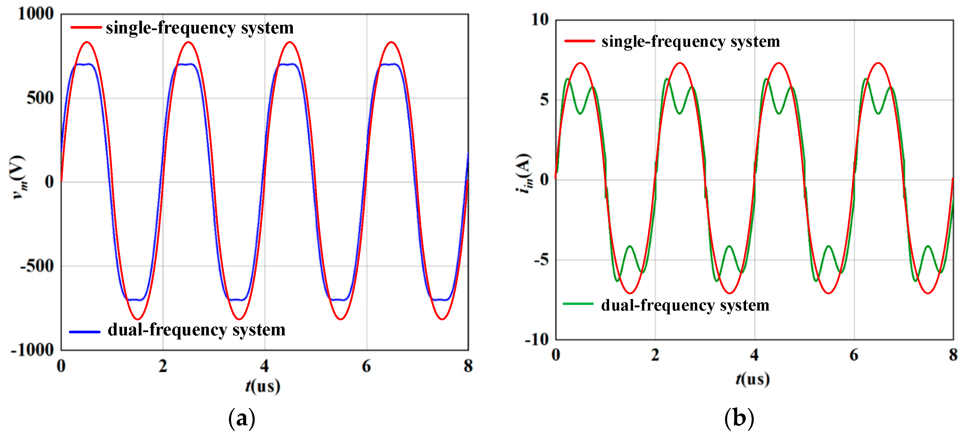
4. Experimental Verification

To verify the above derivation, a test prototype was designed, as shown in Figure 6. The parameters of each component of the system were designed according to Figure 5 and recorded in Table 2. In the actual experimental operation, we used the precision LCR meter in the laboratory to ensure that the actual value of each parameter is as close to the expected value as possible. Coupled plates adopted PCB board design, and Cm = 1.28 nF. The switching frequency of the inverter was selected as 500 kHz. To reduce the influence of the skin effect, a Litz wire containing 1200 strands with a diameter of 0.05 mm was selected. WIMA high-frequency thin-film capacitors were selected to reduce power losses. The inverter was made of CREE silicon carbide (SiC) MOSFETs, and the rectifier was made of Infineon’s SiC diodes.
Figure 7 shows the bode plots of system input admittance. It can be seen that the CPT system can realize the input ZPA characteristics at the two frequencies, 500 kHz and 1500 kHz, and the input admittance is about 0.1 s, meeting the requirements for dual-frequency power transmission.
Figure 8 shows the timing diagram of the system input voltage v i n , input current i i n , coupler voltage v m , and output current i o u t , where (a) is for the simulation test, and (b) is for the experimental test. The waveforms of the input current i i n and coupler voltage v m all show the “peak clipping” effect, which is consistent with the previous theoretical proof and proves the feasibility of using additional third harmonic frequency transmission “channel” to reduce the voltage stress among the coupled plates and the inverter conduction losses.
Figure 9 shows the simulation waveforms of (a) the coupler voltage v m and (b) inverter output current i i n between the proposed dual-frequency system and the equivalent single-frequency system. By comparison, we can see the feasibility of using a dual-frequency system to reduce the voltage stress among the coupled plates and the inverter conduction losses.
Figure 10 shows the output power and efficiency under different inverter input voltages. When the output power is higher than 200 W, the efficiency of the CPT system reaches 83.71%.
Figure 11 shows the waveforms after adding the rectifier structure. We found that the inverter output current waveform appeared distorted, and the system deviated from the resonant state.
As shown in Figure 12, enhanced multiple harmonic analysis (eMHA), a load equivalent method where Z L e q , n = R L e q , n + j X L e q , n , is proposed in [31]. The rectified CPT system is converted into a series of linear systems with complex load impedance, which explains the waveform distortion. In addition, it can be seen from Equation (23) that the voltage stress among the coupled plates of the dual-frequency CPT system is load-independent, so the voltage waveform of the plate is not affected before or after the addition of the rectifier bridge. Therefore, we just need to modify the parameters of Z 4 to bring the system back to the resonant state. Table 3 shows the corrected parameter values.

5. Conclusions

A novel dual-frequency CPT system is proposed in this paper. The goal of reducing the voltage stress among the coupler plates is realized by introducing additional third harmonic voltage components. By controlling the energy transfer ratio of 9:1 ( k = 0.9 ) at the fundamental and third harmonic frequencies, the coupler voltage stress is reduced to 84.3%, and the inverter conduction losses are reduced to 90% of the equivalent single-frequency system. An experimental prototype with a transmission power of 200 W is designed to verify the effectiveness of the proposed dual-frequency CPT system at a system frequency of 500 kHz. The results of the simulation and experiment verify the correctness of the theoretical derivation. In addition, we correct the parameters of Z 4 to make the system return to the resonant state according to eMHA.

Author Contributions

Conceptualization, Y.Z. (Yao Zhang); methodology, S.Y.; software and hardware preparation, Y.Z. (Yiming Zhang) and Y.W.; validation, Z.W.; writing—original draft preparation, S.Y.; writing—review and editing, B.L.; supervision, R.M. All authors have read and agreed to the published version of the manuscript.

Funding

This research received no external funding.

Data Availability Statement

The authors were unable to publish the data set due to privacy restrictions.

Conflicts of Interest

The authors declare no conflict of interest.

References

  1. Zargham, M.; Gulak, P.G. Maximum Achievable Efficiency in Near-Field Coupled Power-Transfer Systems. IEEE Trans. Biomed. Circuits Syst. 2012, 6, 228–245. [Google Scholar] [CrossRef] [PubMed]
  2. Zhu, Z.; Yang, A.; Yuan, H.; Zhao, C.; Chen, F.; Wang, X.; Rong, M. Efficiency Optimization and Power Allocation of Omnidirectional Wireless Power Transfer for Multiple Receivers. IEEE Trans. Ind. Electron. 2022, 1–10. [Google Scholar] [CrossRef]
  3. Yuan, H.; Liang, C.; Zhang, R.; Ruan, Z.; Zhou, Z.; Yang, A.; Wang, X.; Rong, M. A Novel Anti-Offset Interdigital Electrode Capacitive Coupler for Mobile Desktop Charging. IEEE Trans. Power Electron. 2023, 38, 4140–4151. [Google Scholar] [CrossRef]
  4. Wu, Y.; Yuan, H.; Zhang, R.; Yang, A.; Wang, X.; Rong, M. Low-Frequency Wireless Power Transfer Via Rotating Permanent Magnets. IEEE Trans. Ind. Electron. 2022, 69, 10656–10665. [Google Scholar] [CrossRef]
  5. Luo, B.; Hu, A.P.; Munir, H.; Zhu, Q.; Mai, R.; He, Z. Compensation Network Design of CPT Systems for Achieving Maximum Power Transfer Under Coupling Voltage Constraints. IEEE J. Emerg. Sel. Top. Power Electron. 2022, 10, 138–148. [Google Scholar] [CrossRef]
  6. Luo, B.; Long, T.; Guo, L.; Dai, R.; Mai, R.; He, Z. Analysis and Design of Inductive and Capacitive Hybrid Wireless Power 462 Transfer System for Railway Application. IEEE Trans. Ind. Appl. 2020, 56, 3034–3042. [Google Scholar] [CrossRef]
  7. Liu, W.; Luo, B.; He, X.; Wang, Z.; Mai, R. Analysis of Compensation Topology with Constant-Voltage/Current Output for Multiple Loads Capacitive Power Transfer System. CSEE J. Power Energy Syst. 2023, 1–12. [Google Scholar] [CrossRef]
  8. Zhang, Z.; Pang, H.; Georgiadis, A.; Cecati, C. Wireless power transfer—An overview. IEEE Trans. Ind. Electron. 2019, 2, 1044–1058. [Google Scholar] [CrossRef]
  9. Lu, F.; Zhang, H.; Mi, C. A Review on the Recent Development of Capacitive Wireless Power Transfer Technology. Energies 2017, 10, 1752. [Google Scholar] [CrossRef] [Green Version]
  10. Lian, J.; Qu, X. Design of a Double-Sided LC Compensated Capacitive Power Transfer System With Capacitor Voltage Stress Optimization. IEEE Trans. Circuits Syst. II Express Briefs 2020, 67, 715–719. [Google Scholar] [CrossRef]
  11. Liang, H.W.R.; Wang, H.; Lee, C.-K.; Hui, S.Y.R. Analysis and Performance Enhancement of Wireless Power Transfer Systems With Intended Metallic Objects. IEEE Trans. Power Electron. 2021, 36, 1388–1398. [Google Scholar] [CrossRef]
  12. Shah, I.A.; Yoo, H. Assessing Human Exposure With Medical Implants to Electromagnetic Fields From a Wireless Power Transmission System in an Electric Vehicle. IEEE Trans. Electromagn. Compat. 2020, 62, 338–345. [Google Scholar] [CrossRef]
  13. Jegadeesan, R.; Agarwal, K.; Guo, Y.-X.; Yen, S.-C.; Thakor, N.V. Wireless Power Delivery to Flexible Subcutaneous Implants Using Capacitive Coupling. IEEE Trans. Microw. Theory Tech. 2017, 65, 280–292. [Google Scholar] [CrossRef]
  14. Erfani, R.; Marefat, F.; Sodagar, A.M.; Mohseni, P. Modeling and Experimental Validation of a Capacitive Link for Wireless Power Transfer to Biomedical Implants. IEEE Trans. Circuits Syst. II Express Briefs 2018, 65, 923–927. [Google Scholar] [CrossRef]
  15. Erfani, R.; Marefat, F.; Sodagar, A.M.; Mohseni, P. Modeling and Characterization of Capacitive Elements with Tissue as Dielectric Material for Wireless Powering of Neural Implants. IEEE Trans. Neural Syst. Rehabil. Eng. 2018, 26, 1093–1099. [Google Scholar] [CrossRef]
  16. Erfani, R.; Marefat, F.; Nag, S.; Mohseni, P. A 1–10-MHz Frequency-Aware CMOS Active Rectifier With Dual-Loop Adaptive Delay Compensation and >230-MW Output Power for Capacitively Powered Biomedical Implants. IEEE J. Solid-State Circuits 2020, 55, 756–766. [Google Scholar] [CrossRef]
  17. Lu, F.; Zhang, H.; Hofmann, H.; Mi, C. A Double-Sided LCLC-Compensated Capacitive Power Transfer System for Electric Vehicle Charging. IEEE Trans. Power Electron. 2015, 30, 6011–6014. [Google Scholar] [CrossRef]
  18. Doubleday, K.; Kumar, A.; Regensburger, B.; Pervaiz, S.; Sinha, S.; Popovic, Z.; Afridi, K.K. Multi-Objective Optimization of Capacitive Wireless Power Transfer Systems for Electric Vehicle Charging. In Proceedings of the 2017 IEEE 18th Workshop on Control and Modeling for Power Electronics (COMPEL), Stanford, CA, USA, 21 August 2017. [Google Scholar]
  19. Dai, J.; Ludois, D.C. Capacitive Power Transfer Through a Conformal Bumper for Electric Vehicle Charging. IEEE J. Emerg. Selected Top. Power Electron. 2016, 4, 1015–1025. [Google Scholar] [CrossRef]
  20. Ohira, T. A Battery-Less Electric Roadway Vehicle Runs for the First Time in the World. In Proceedings of the 2017 IEEE MTT-S International Conference on Microwaves for Intelligent Mobility (ICMIM), Nagoya, Japan, 4 May 2017. [Google Scholar]
  21. Li, S.; Liu, Z.; Zhao, H.; Zhu, L.; Shuai, C.; Chen, Z. Wireless Power Transfer by Electric Field Resonance and Its Application in Dynamic Charging. IEEE Trans. Ind. Electron. 2016, 63, 6602–6612. [Google Scholar] [CrossRef]
  22. Liu, W.; Luo, B.; Xu, Y.; Pan, S.; Zhou, W.; Jiang, C.; Mai, R. A Multi-Load Capacitive Power Transfer System with Load-Independent Characteristic for Reefer Container Application. IEEE Trans. Power Electron. 2022, 37, 6194–6205. [Google Scholar] [CrossRef]
  23. Ludois, D.C.; Reed, J.K.; Hanson, K. Capacitive Power Transfer for Rotor Field Current in Synchronous Machines. IEEE Trans. Power Electron. 2012, 27, 4638–4645. [Google Scholar] [CrossRef]
  24. Erel, M.Z.; Bayindir, K.C.; Aydemir, M.T.; Chaudhary, S.K.; Guerrero, J.M. A Comprehensive Review on Wireless Capacitive Power Transfer Technology: Fundamentals and Applications. IEEE Access 2022, 10, 3116–3143. [Google Scholar] [CrossRef]
  25. Ludois, D.C.; Erickson, M.J.; Reed, J.K. Aerodynamic Fluid Bearings for Translational and Rotating Capacitors in Noncontact Capacitive Power Transfer Systems. IEEE Trans. Ind. Appl. 2014, 50, 1025–1033. [Google Scholar] [CrossRef]
  26. Mai, R.; Luo, B.; Chen, Y.; He, Z. Double-sided CL Compensation Topology Based Component Voltage Stress Optimisation Method for Capacitive Power Transfer Charging System. IET Power Electron. 2018, 11, 1153–1160. [Google Scholar] [CrossRef]
  27. Pantic, Z.; Lee, K.; Lukic, S.M. Multifrequency Inductive Power Transfer. IEEE Trans. Power Electron. 2014, 29, 5995–6005. [Google Scholar] [CrossRef]
  28. Gao, X.; Du, B.; Zhang, Y.; Cui, S. A Dual-Frequency Compatible Wireless Power Transfer System with a Single Transmitter and Multiple Receivers. IEEE Access 2022, 10, 102564–102574. [Google Scholar] [CrossRef]
  29. Zhang, Z.; Li, X.; Pang, H.; Komurcugil, H.; Liang, Z.; Kennel, R. Multiple-Frequency Resonating Compensation for Multichannel Transmission of Wireless Power Transfer. IEEE Trans. Power Electron. 2021, 36, 5169–5180. [Google Scholar] [CrossRef]
  30. Qi, C.; Miao, H.; Lang, Z.; Chen, X. A Generalized Methodology to Generate, Amplify and Compensate Multi-Frequency Power for a Single-Inverter-Based MF-MR-S-WPT System. IEEE Access 2020, 8, 181513–181525. [Google Scholar] [CrossRef]
  31. Fang, Y.; Pong, B.M.H.; Hui, R.S.Y. An Enhanced Multiple Harmonics Analysis Method for Wireless Power Transfer Systems. IEEE Trans. Power Electron. 2020, 35, 1205–1216. [Google Scholar] [CrossRef]
Figure 1. The fundamental and third harmonic frequencies’ superimposed wave cluster.
Electronics 12 01274 g001
Figure 2. (a) Dual-frequency CPT system schematic. (b) Compensation unit model [27]. (c) Dual-frequency CPT system Π-type equivalent circuit model. (d) Dual-frequency CPT system T-type equivalent circuit model.
Electronics 12 01274 g002
Figure 3. Relationship between normalized coupler voltage V m , d , m a x * and power-sharing ratio k.
Electronics 12 01274 g003
Figure 4. Relationship between normalized inverter conduction losses P i n l o s s , d * and power-sharing ratio k .
Electronics 12 01274 g004
Figure 5. Design flowchart of the dual-frequency CPT system.
Electronics 12 01274 g005
Figure 6. Experimental prototype of the proposed CPT system.
Electronics 12 01274 g006
Figure 7. Experimental prototype of the proposed CPT system.
Electronics 12 01274 g007
Figure 8. Waveforms of input voltage v i n , input current i i n , coupler voltage v m , and output current i o u t for the dual-frequency CPT system in the (a) simulation test and (b) experimental test.
Electronics 12 01274 g008
Figure 9. Waveforms of (a) the coupler voltage v m and (b) inverter output current i i n for the proposed dual-frequency system and the equivalent single-frequency system.
Electronics 12 01274 g009
Figure 10. System output power and efficiency versus V d c .
Electronics 12 01274 g010
Figure 11. Waveforms of input voltage v i n , input current i i n , coupler voltage v m , and output current i o u t after adding the rectifier structure.
Electronics 12 01274 g011
Figure 12. The transformation from original load to multiple harmonics model.
Electronics 12 01274 g012
Table 1. V m , d , m a x and P i n l o s s , d of the system under different conditions.
k V m , d , m a x P i n l o s s , d
0 0.333 · 2 V m , s 9 P i n l o s s , s
0.2 0.594 · 2 V m , s 5.8 P i n l o s s , s
0.4 0.632 · 2 V m , s 3.4 P i n l o s s , s
0.6 0.7 · 2 V m , s 1.8 P i n l o s s , s
0.8 0.775 · 2 V m , s P i n l o s s , s
0.9 0.843 · 2 V m , s 0.9 P i n l o s s , s
1 2 V m , s P i n l o s s , s
Table 2. Parameters of the experimental setup.
ParameterValueParameterValue
Input DC Voltage50 V C m 1.28 nF
Switching Frequency500 kHz L 3 21.6 µH
L 1 3 µH C 3 787 pF
C 1 11.64 nF L 3 50 µH
C 1 8.8 nF L 4 29.15 µH
L 2 2.1 µH C 4 7.12 nF
C 2 18.19 nF C 4 816 pF
L 2 3 µH R L 40 Ω
Table 3. Parameters of the corrected system.
Parameter L 4 C 4 C 4
Original Value29.15 µH7.12 nF816 pF
Corrected Value3.3 µH12.7 nF626 pF
Disclaimer/Publisher’s Note: The statements, opinions and data contained in all publications are solely those of the individual author(s) and contributor(s) and not of MDPI and/or the editor(s). MDPI and/or the editor(s) disclaim responsibility for any injury to people or property resulting from any ideas, methods, instructions or products referred to in the content.

