Communication

High-Performance QC-LDPC Code Co-Processing Approach and VLSI Architecture for Wi-Fi 6

1
Institute of Microelectronics of the Chinese Academy of Sciences, Beijing 100029, China
2
School of Microelectronics, University of Chinese Academy of Sciences, Beijing 100049, China
3
CASEMIC Electronics Technology Co., Ltd., Hangzhou 310051, China
*
Author to whom correspondence should be addressed.
Electronics 2023, 12(5), 1210; https://doi.org/10.3390/electronics12051210
Submission received: 30 January 2023 / Revised: 1 March 2023 / Accepted: 2 March 2023 / Published: 3 March 2023
(This article belongs to the Special Issue Advanced Digital Signal Processing for Future Digital Communications)

Abstract

:
The QC-LDPC code, with its excellent error correction performance and hardware friendliness, has been identified as one of the channel encoding schemes by Wi-Fi 6. Shorting, puncturing, or repeating operations are needed to ensure that user data can be sent with integer symbols and complete rate matching. Due to the uncertainty of the user data size, the modulation’s selectivity, and the difference in the number of spatial streams, the receiver must deal with more than 106 situations. At the same time, other computationally intensive tasks occupy the time slot budget of the receiver. Typical are demodulation and decoding. Hence, the receiver needs to quickly reverse the demodulated data process. This paper first proposes a co-processing method and VLSI architecture compatible with all code lengths, code rates, and processing parameters. The co-processor separates field and block splicing, simplifying the control logic. There is no throughput rate bottleneck, and the maximum delay is less than 1 us.

Graphical Abstract

1. Introduction

Quasi-Cyclic Low-Density Parity-Check (QC-LDPC) codes have been widely used in wireless communication protocols, with their excellent error correction performance and relative ease of implementation. Like the Wireless Local Area Network (WLAN) series protocol IEEE 802.11n/ac/ax, the QC-LDPC encoding scheme of the Data Field (DF) is optional in IEEE 802.11n/ac [1]. Furthermore, in IEEE 802.11ax, it is stipulated that only QC-LDPC encoding can be used when the modulation method is 1024 Quadrature Amplitude Modulation (QAM) or the resource units are more significant than 484 [2]. To ensure that the encoded data can be sent in a string of integer symbols and the rate matches, different protocols adopt their processing characteristics. If the amount of data to be sent in IEEE 802.16e is less than the allocated amount, redundant ones are added at the end of the data [3]. For 5G NR, the bit sequence after encoding is written into a circular buffer and combines with the Hybrid Automatic Repeat Request (HARQ) to complete the rate matching [4]. For the WLAN, exact symbol matching is carried out by pre-processing before encoding and post-processing after encoding. Pre- and post-processing can be collectively referred to as co-processing. Decoding is the inverse process of encoding. The decoder’s pre-processing and post-processing correspond to the encoder’s post-processing and pre-processing. The difference is that the acquisition of the decoding parameters depends on the parsing of the received frame. Taking the decoder as an example, after the receiver completes the demodulation to obtain the soft information of the DF, the pre-processing module adds the shortened bits and punctured bits or removes the repeated bits according to the given parameters, and spells out a series of complete codewords to the decoder core. The post-processing module extracts pure Physical Layer Service Data Unit (PSDU) data from the information bits in the codewords when the decoding is completed. In the actual processing process, due to the uncertainty of user data size and the selectivity of modulation mode and spatial stream number, Wi-Fi 6 co-processing needs to deal with more than 106 situations. At the same time, the time slot budget needs to be allocated to compute-intensive tasks such as demodulation and decoding, and the overall latency of the co-processor is less than 1us, which brings challenges to the circuit design of co-processing.
Although wireless communication protocols widely use co-processing, and its theoretical research is endless, there has been no research on co-processing implementation [5,6,7]. J. Yongmin mentioned coprocessing in his encoder architecture, but did not give a specific implementation [8]. This paper first proposes a QC-LDPC code co-processing method and VLSI architecture for Wi-Fi 6, which can be compatible with all possible protocol scenarios through reasonable hierarchical division and field analysis. Through the ping-pong operation of the block splicing module, the problem of practical input across blocks is solved. This paper is organized as follows: Section 2 introduces the decoder’s parameter calculation and decoding process. Section 3 presents the methods and architectures for pre-processing and post-processing of decoders. Section 4 gives the implementation results, and Section 5 provides a summary.

2. Decoding Process and Parameters Calculation of the Decoder

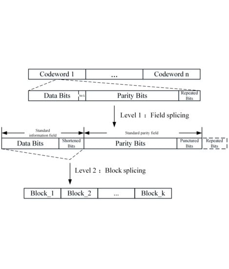
2.1. Decoding Process

The DF received by the decoder is shown in Figure 1, consisting of a series of codewords. Each codeword includes the actual information field Data Bits (DBs), the check field Parity Bits (PBs) obtained from the parity check matrices, and the replica field Repeated Bits (RBs) that may exist. Each bit of these fields is typically populated by a log-likelihood ratio (LLR) soft information of the intrinsic channel observations.
The decoding process can be divided into three stages: pre-processing, decoding, and post-processing. According to the calculated parameters, the preprocessor will stitch the received fields into a complete codeword required by the decoding core; the output fields are shown in Figure 2. First, the preprocessor needs to append shortened bits that the encoding phase may use to populate the specified length to the standard information field (SIF). If the repeated bits exist, the preprocessor must remove the replica field that the encoder added after the codeword. Furthermore, if the punctured bits are present, the codeword needs to be padded at the end of the check field, and since the deleted bits are indeterminate, the LLRs value of the padding is zero.
The decoding stage decodes the fields in Figure 2 into the soft information field. A reliable soft information field is obtained through the iterative propagation of the message. Many scholars have worked to achieve the best trade-offs between latency, resource overhead, throughput, and power consumption [9,10]. The post-processing phase removes the possible SBs and only retains the valid information field DBs needed by the medium access control (MAC).

2.2. Co-Processing Parameter Calculation

This paper takes a single user (multiple users each perform the corresponding operation) as an example and briefly introduces the parameter calculation process.

2.2.1. Calculate the Real Number of Symbols NSYM and the Number of Available Bits Navbits

For the reception, the NSYM needs to be computed through the following three steps. Firstly, the received symbol duration RXTIME is first calculated based on the L-LENGTH in the L-SIG field:
R X T I M E ( u s ) = L _ L E N G T H + 3 3 × 4 + 20
Secondly, the proper duration of the DF is obtained according to the total symbol duration and time of other fixed fields. Then, it can be divided by the period of the individual symbols Tsym to convey the symbol of the DF field N’SYM.
N S Y M = R X T I M E T o t h e r _ f i e l d s T s y m
Taking the usage of space-time block code (STBC) and extra symbol (ES) into account, the number of symbols for proper LDPC decoding NSYM is finally obtained according to Equation (3).
N S Y M = N S Y M         ES = 0 N S Y M 1         ES = 1 ,     STBC = 0 N S Y M 2         ES = 1 ,     STBC = 1
Finally, according to the number of symbols NSYM, the number of bits in the PSDU and SERVICE field Npld and the number of available bits Navbits carried by the symbols can be calculated.
N a v b i t s = N p l d = N s y m × N d b p s

2.2.2. Compute the Number and Length of the Codewords

The number of codewords NCW to be transmitted and the length of the codewords LLDPC to be used can be calculated from Table 1. Where R repeats the code rate.

2.2.3. Calculate the SBs, PBs, and RBs

From NCW, Navbits, LLDPC, and R, the SBs Nshrt, PBs Npunc, and RBs Nrep are obtained according to Equations (5)–(7). The Npunc may need to recompute with increment Navbits [1].
N s h r t = max ( 0 , ( N C W × L L D P C × R ) N p l d )
N p u n c = max ( 0 , ( N C W × L L D P C ) N a v b i t s N p l d )
N r e p = max ( 0 , N a v b i t s N C W × L L D P C × ( 1 R ) N p l d )

3. The Co-Processing Schemes and Architectures

3.1. The Strategy and Architecture of Pre-Processing

The preprocessor’s architecture, as shown in Figure 3, consists of the input cache: Input Buffer (IB), the Block Splicing (BS), the output cache: Output Buffer (OB), and the global controller: Global Control (GC). The external module gives LDPC-related parameters (usually provided by the baseband frame parsing module, which is not discussed in this paper) and LLRs information. The preprocessor first stores the LLRs information in the IB. The highest modulation, the maximum number of antenna streams Nss, and the quantization of the bit width Q determine the bit width size of the IB, and the bit width sizes in various configurations are shown in Table 2. Suppose the maximum modulation supported by the system is 256 QAM, and the maximum number of antenna streams is two, taking the dual-stream Quadrature Phase Shift Keying (QPSK) as an example. In that case, the input data format is shown in Figure 4. Where in the effective bit widths dins1_1, dins1_2, dins2_1, and dins2_2 represent the soft information of the 1st bit, the 2nd bit in antenna 1, the 1st bit, the 2nd bit in the antenna 2, respectively. The number of effective bits may be less than the maximum bit widths to maintain pattern compatibility, and the remaining bits can be filled with zero.
If the OB is not whole and the IB is not empty, the preprocessor starts taking data from IB and stitching fields. Since the QC-LDPC code is a linear block grouping code, the output data format of the pre-processing module is continuous output by block. Furthermore, considering the compatibility of the length of the codewords, the output bit width is unified to the maximum bit width, 81 × Q. However, because the bit width size of the IB is fixed, field stitching and block stitching are mixed, the control is highly complex, and it is not easy to ensure complete coverage of all possible scenarios. Based on this, this paper proposes a structure in which field splicing and block splicing are separated, the top-level control state machine is only for field splicing, and the BS completes the block splicing.
Taking a codeword in a frame as an example, the critical points of field stitching are as follows. DBs: Firstly, the length of SBs for the current codeword is needed. Using the total number of SBs Nshrt and NCW, the quotient and the remainder of the SBs are obtained by division. If the ordinal number of the current codeword is less than or equal to the rest, the size of SBs is the quotient plus one, and vice versa, is equal to the quotient. The actual length of DBs can be obtained by subtracting the size of SBs from the SIF length. The output data of the IB of the last codeword may have a residue connected to the end of the PBs or the RBs. If PUBs are not zero, the residual number is written to the DBs of the current codeword before the remaining length of the DBs is taken from IB, as shown in case 1 in Figure 5. If the RBs are not zero, the RBs in the IB output data needs to be discarded. Next, the residual widths are written to the DBs, and the remaining lengths of the DBs are continuously taken out of the IB, as shown in case 2 in Figure 5.
SBs: If the SBs for current codewords are not null, they should be padded with zero of the corresponding length at the end of DBs. If the quantization bit width is 7, the related soft information is +63 (determined to be zero), the sign bit is filled with zero, and the other bits are filled with one. When implemented, a control signal can be given so that the block splicing module will fill the remaining bits of the current block with zero. Suppose the SBs of the codeword are more significant than the block size. In that case, the block splicing module continues to output all zero blocks until the number of output blocks reaches the number of standard information blocks corresponding to the current code rate.
PBs: The processing of the PBs is similar to the DBs. First, according to the total number of PUBs Npunc, the NCW, the current codeword order, and the length of the standard PBs, the actual PBs are determined. Similarly, if there is a residual width in the final output of IB for the DBs, the remaining bits are written before the number of remaining PBs is taken from the IB.
PUBs: If the PUBs are not null, it is filled with indeterminate data of the corresponding length, corresponding to zero value for the soft information. The detailed implementation is similar to the SBs.
RBs: If the RBs are exited, the length of the RBs of the current codeword is determined based on the total number of RBs Nrep, the NCW, and the ordinal number of the current codeword. If residual widths exist in the last IB output data widths for the PBs, the residual data are discarded before the remaining RBs lengths are read out of the IB. In the case of higher modulation, such as 1024 QAM, it may be possible for an output of IB to contain both the PBs, the RBs, and the DBs for the next codeword.
To this end, this paper designs the state flow diagram shown in Figure 6, which is divided into the following six states:
IDLE1: idle
INFOR: IF processing
SHORT: SBs processing
PARITY: PBs processing
PUNC: PUBs processing
REPT: RBs processing
Where:
statrt1: the start of field processing. Four conditions determine it: there are remaining codewords in this frame, the ready signal that the decoding core has prepared, the IB is not empty, and there are no residual bits to be processed.
len_if_cnt: length of the remaining pending IF.
w_ib: the output width of the IB.
b_if _cnt: the number of blocks of the IF to be processed.
len_p: length of PUBs.
len_r: the size of RPs.
len_r_cnt: length of the remaining pending RPs.
b_cnt: the number of blocks to be processed.
Block stitching is the next layer of field stitching, and block stitching is carried out based on the output of the IB and the corresponding valid bit length. Figure 7 shows the state diagram, with a total of seven states:
IDLE2: idle
WR_B: general block stitching
REPT: RPs processing
SH_PD: SBs padding
SH_B: SBs full block padding
PU_PD: PUBs padding
PU_B: PUBs full block padding
Thereinto:
start2: the start of block splicing, and valid when start1 is valid, or there is a residual bit, that is start 2 = start 1 | | res _ bits .
state 1: the state of field splicing
p_pd: the first block padding of PUBs is complete
s_pd: the first block padding of SBs is complete
It is worth noting that len_p and len_r cannot be greater than zero at the same time. Because when we conduct rate matching, we can only delete a part of the bits (punctured) or add a part (repeated) to adapt to the communication system integer symbol transmitting and receiving.
The valid bit length may be cross-block, as shown in Figure 8. This paper adopts a ping-pong structure, two sets of shift registers, and alternately outputs the spliced blocks. As shown in Figure 8, the valid inputs at clock cycle i are x1, x2, x3, and x4, where x1, x2 fill the current block (Registers Group1) by shifting left and x3, x4 shift left to write another set of registers (Registers Group2). In processing the SBs, the symbol bits, and the numeric bits are filled with different values, and two submodules can complete the filling of the symbol bits and the numeric bits, respectively.
Whenever a block is spliced, the block stitching module writes the block to the OB, the depths of which are set to 24; i.e., the total number of blocks of a codeword. When the idle indication of the decoding core module and the OB is whole, it is transmitted to the decoding core module in burst mode. In general, in addition to the first time the output cache is filled, the decoding iteration time is sufficient for the OB to fill up, so the delay in increasing the link is equivalent to the first fill time. In the case of high modulation, the pre-processing module only requires a few dozen clock cycles to meet the low latency requirements of the link.

3.2. Post-Processing Strategy and Architecture

After the decoding phase is over, the decoding core module outputs the SIF to the post-processing module. The post-processing module deletes the SBs in the SIF and outputs them to the backing stage according to the specified bit width, as shown in Figure 9.

4. Implementation Results

The Register Transfer Level (RTL) models for the proposed preprocessor and postprocessor hardware architecture are designed with Verilog HDL and synthesized with the Semiconductor Manufacturing International Corporation (SMIC) 55 nm Complementary Metal Oxide Semiconductor (CMOS) process. A summary of the implementation results is presented in Table 3. It can be seen from the table that the preprocessor accounts for 95.8% of the overall resources, the internal resources of the processing module are mainly distributed to IB, OB, and BS modules, and the GC module accounts for a relatively small amount. The maximum clock frequency of the co-processor is 1 GHz, and the theoretical maximum throughput rate is 16 Gbps. This far exceeds the maximum standard throughput rate of 2401.9 Mbps (resource block RU = 2 × 996, protection interval GI = 0.8 us) of dual-stream 1024 QAM, so there is no throughput rate neck.

5. Conclusions

This paper first proposes a QC-LDPC code, co-processing method, and VLSI architecture for Wi-Fi 6 chips. Through field splicing and block splicing, the strategy and architecture are compatible with all possible protocol modes (>106). The corresponding implementation result shows the co-processor enables a maximum throughput of 16 Gbps, a maximum latency of less than 1 us, a hardware complexity of 136 kGE, and can flexibly scale to future 8-space streams and 16-space streams.

Author Contributions

Conceptualization, B.W.; methodology, Y.W.; implementation, Y.W.; writing-original, Y.W.; writing-review and editing, X.Z. All authors have read and agreed to the published version of the manuscript.

Funding

This research received no external funding.

Data Availability Statement

The RTL codes of the co-processor can be found at: https://pan.baidu.com/s/1lK9gRxO0vE-5RnJf02hg6Q?pwd=t2g4.w (access on 1 January 2023).

Conflicts of Interest

The authors declare no conflict of interest.

References

  1. IEEE, 802.11-2016; Standard for Information Technology—Local and Metropolitan Area Networks—Specific Requirements—Part 11: Wireless LAN Medium Access Control (MAC) and Physical Layer (PHY) Specifications. IEEE Standard Association: Piscataway, NJ, USA, 2016.
  2. IEEE, 802.11ax-2021; Standard for Information Technology—Telecommunications and Information Exchange between Systems Local and Metropolitan Area Networks—Specific Requirements Part 11: Wireless LAN Medium Access Control (MAC) and Physical Layer (PHY) Specifications Amendment 1: Enhancements for High-Efficiency WLAN. IEEE Standard Association: Piscataway, NJ, USA, 2021; pp. 1–767.
  3. IEEE, 802.16-2004; Standard for Local and Metropolitan Area Networks—Part 16: Air Interface for Fixed Broadband Wireless Access Systems. IEEE Standard Association: Piscataway, NJ, USA, 2004.
  4. 3GPP TS 38.212 V16.1.0 (2020–03); 3rd Generation Partnership Project; Technical Specification Group Radio Access Network; NR. Multiplexing and channel coding (Release 16). ETSI: Sophia Antipolis, France, 2020.
  5. Suls, A.; Lefevre, Y.; Van Hecke, J.; Guenach, M.; Moeneclaey, M. Error Performance Prediction of Randomly Shortened and Punctured LDPC Codes. IEEE Commun. Lett. 2019, 23, 560–563. [Google Scholar] [CrossRef]
  6. Beermann, M.; Beermann, V.P. Joint optimization of multi-rate LDPC code ensembles for the AWGN channel based on shortening and puncturing. In Proceedings of the 2014 IEEE Wireless Communications and Networking Conference (WCNC), Istanbul, Turkey, 20 November 2014; pp. 200–205.
  7. Asvadi, R.; Banihashemi, A.H. A Rate-Compatible Puncturing Scheme for Finite-Length LDPC Codes. IEEE Commun. Lett. 2013, 17, 147–150. [Google Scholar] [CrossRef]
  8. Yongmin, J.; Chulho, C.; Jaeseok, K.; Yunho, J. 7.7 Gbps encoder design for IEEE 802.11n/ac QC-LDPC codes. In Proceedings of the 2012 International SoC Design Conference (ISOCC), Jeju Island, Replublic of Korea, 4–7 November 2012; pp. 215–218. [Google Scholar]
  9. Tsatsaragkos, I.; Paliouras, V. A Reconfigurable LDPC Decoder Optimized for 802.11n/ac Applications. IEEE Trans. Very Large Scale Integr. (VLSI) Syst. 2018, 26, 182–195. [Google Scholar] [CrossRef]
  10. Roberts, M.K.; Jayabalan, R. An area efficient and high throughput multi-rate quasi-cyclic LDPC decoder for IEEE 802.11n applications. Microelectron. J. 2014, 45, 1489–1498. [Google Scholar] [CrossRef]
Figure 1. Data received by the decoder.
Electronics 12 01210 g001
Figure 2. Pre-processed fields.
Electronics 12 01210 g002
Figure 3. Preprocessor Architecture.
Electronics 12 01210 g003
Figure 4. The data format of the input buffer.
Electronics 12 01210 g004
Figure 5. Input buffer output residual bits.
Electronics 12 01210 g005
Figure 6. State diagram of field splicing.
Electronics 12 01210 g006
Figure 7. State diagram of block splicing.
Electronics 12 01210 g007
Figure 8. Valid input bits span blocks.
Electronics 12 01210 g008
Figure 9. Postprocessor Architecture.
Electronics 12 01210 g009
Table 1. The number and length of codewords.
Range of Navbits (bits)NCWLLDPC (bits)
N a v b i t s 648 .11296, if N a v b i t s N p l d + 912 × ( 1 R ) 648, otherwise
648 < N a v b i t s 1296 11944, if N a v b i t s N p l d + 1464 × ( 1 R ) 1296, otherwise
1296 < N a v b i t s 1944 11944
1944 < N a v b i t s 2592 21944, if N a v b i t s N p l d + 2916 × ( 1 R ) 1296, otherwise
2592 < N a v b i t s N p l d 1944 × R 1944
Table 2. The bit width of the input buffer.
NssBPSKQPSK16QAM64QAM256QAM1024QAM
1QQ2 × Q4 × Q6 × Q8 × Q
22 × Q2 × Q4 × Q8 × Q12 × Q16 × Q
...............
88 × Q8 × Q16 × Q32 × Q48 × Q64 × Q
Table 3. Hardware complexity of the proposed implementation.
ComponentArea (mm2)Complexity (kGE 1)Percentage (%)
Block Stitching0.079 61.91 45.52
Input Buffer0.046 35.73 26.28
Output Buffer0.037 28.63 21.05
Global Control0.005 4.01 2.95
Preprocessor0.167 130.28 95.80
Global Control20.001 1.01 0.74
Input Buffer20.005 3.88 2.85
Bit Width Converter0.002 1.32 0.97
Postprocessor0.008 6.21 4.56
Total0.175 136.49 100
1 One gate equivalent (GE) corresponds to the area of a two-input drive-one NAND gate of size 1.28 um2.
Disclaimer/Publisher’s Note: The statements, opinions and data contained in all publications are solely those of the individual author(s) and contributor(s) and not of MDPI and/or the editor(s). MDPI and/or the editor(s) disclaim responsibility for any injury to people or property resulting from any ideas, methods, instructions or products referred to in the content.

