

Carbon Electrodes: The Rising Star for PSC Commercialization

Abstract
:1. Introduction
2. Background
2.1. Dye-Sensitized Solar Cells (DSSCs)
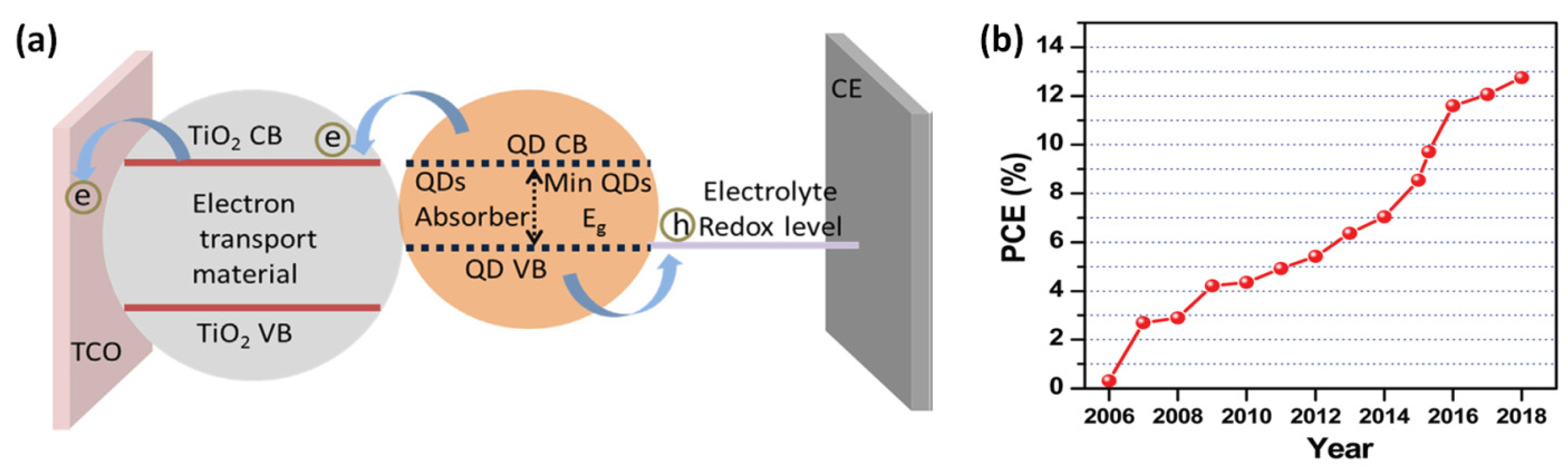
2.2. Quantum-Dot-Sensitized Solar Cells (QD-SSCs)
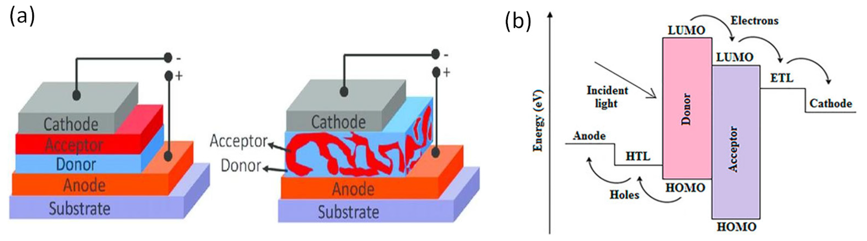
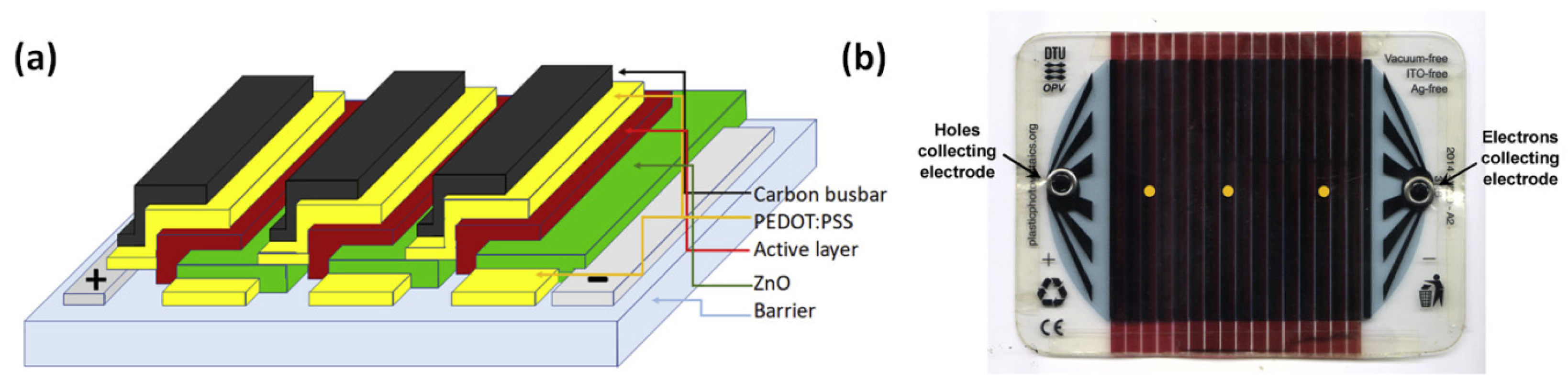
2.3. Organic Photovoltaics (OPVs)
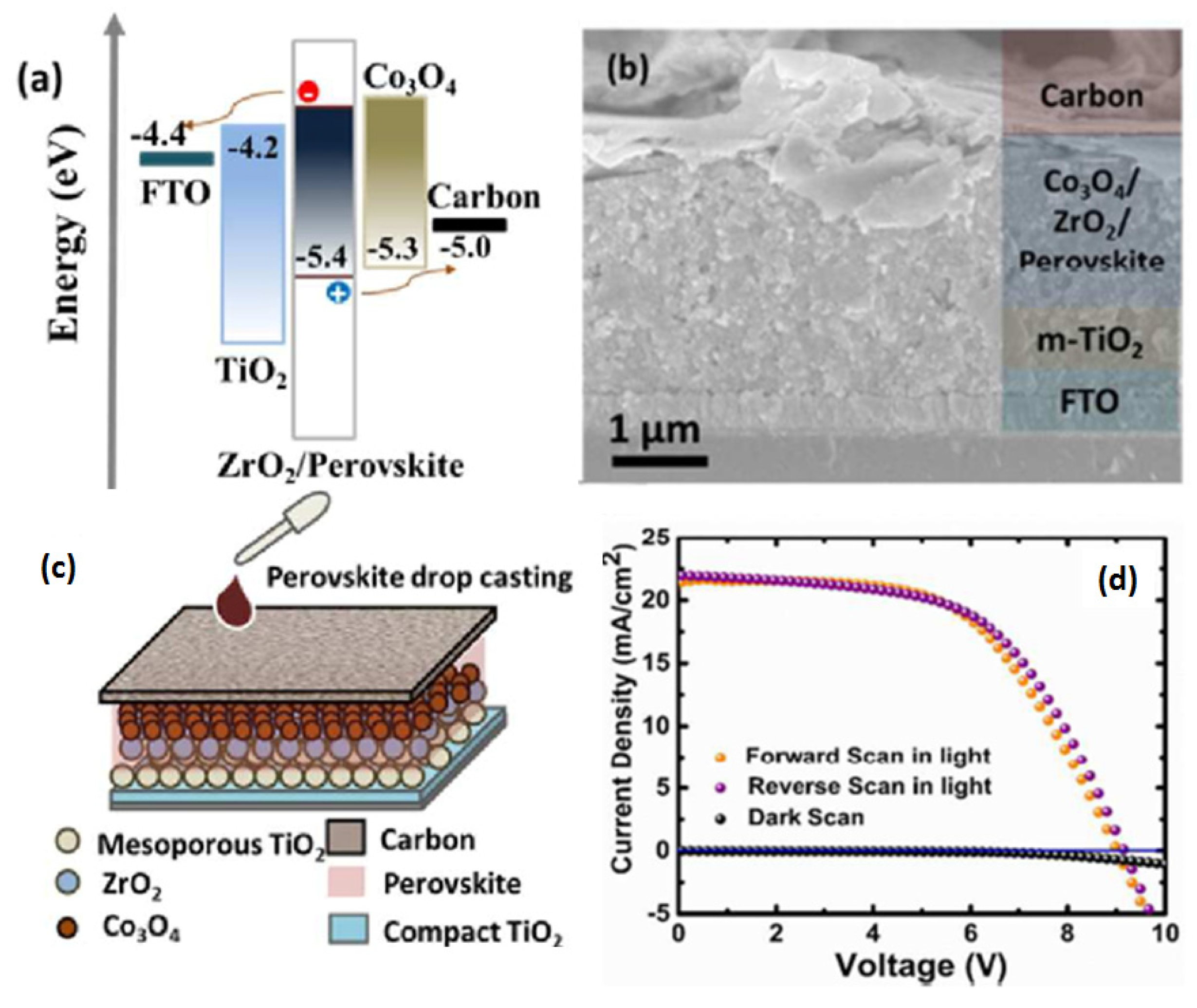
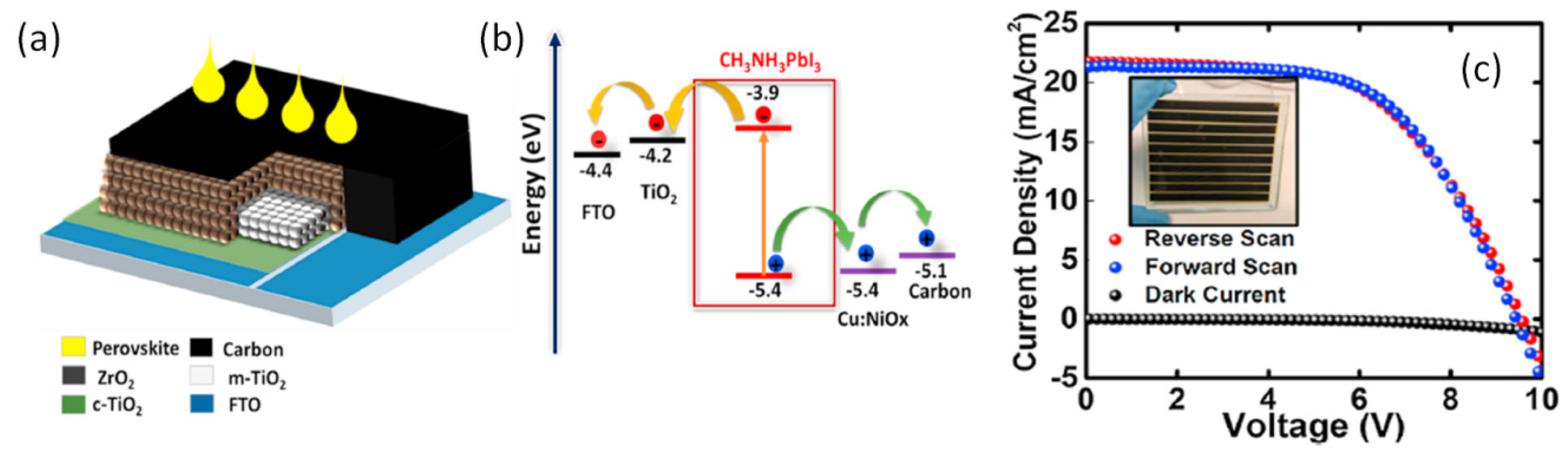
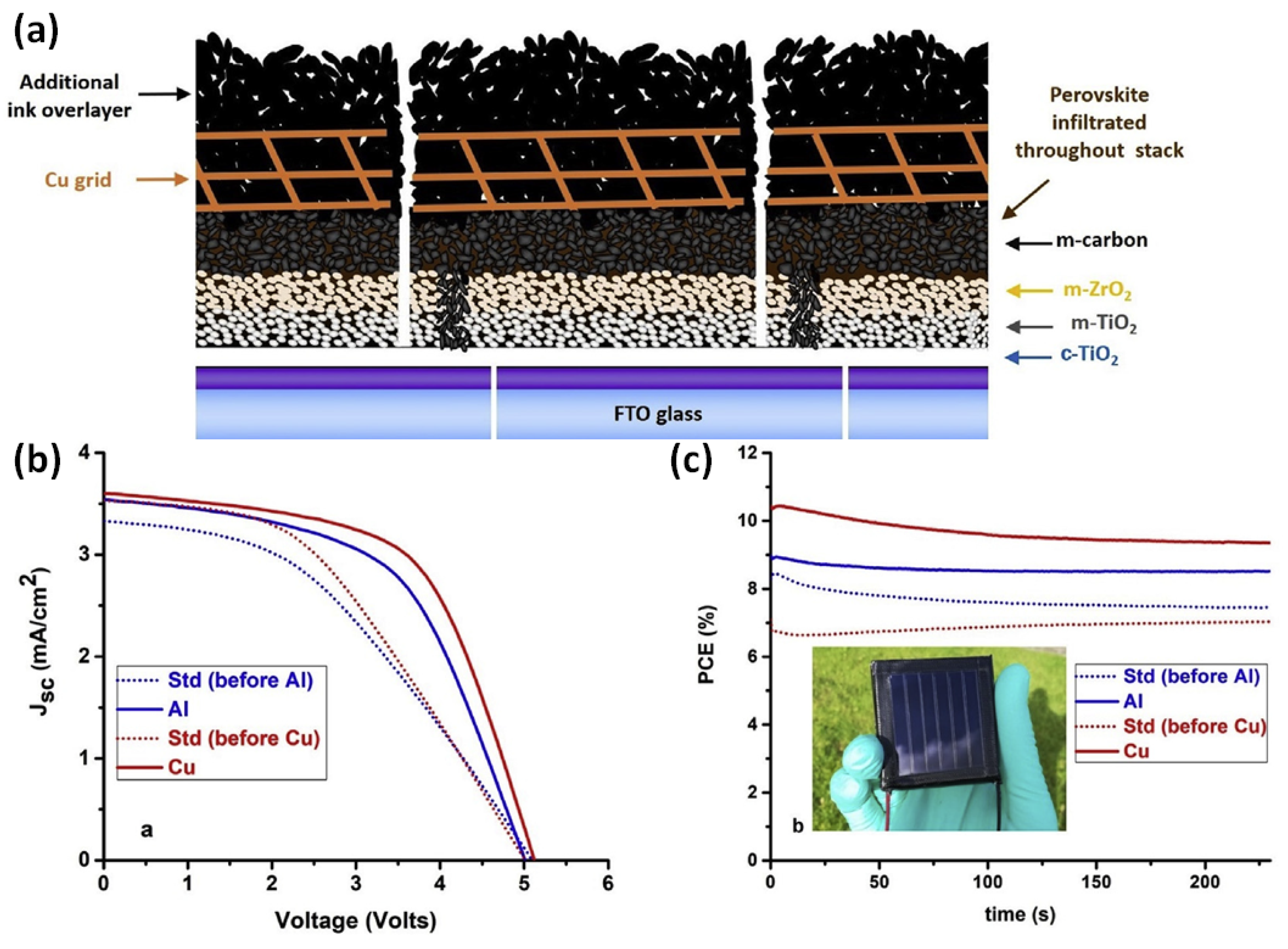
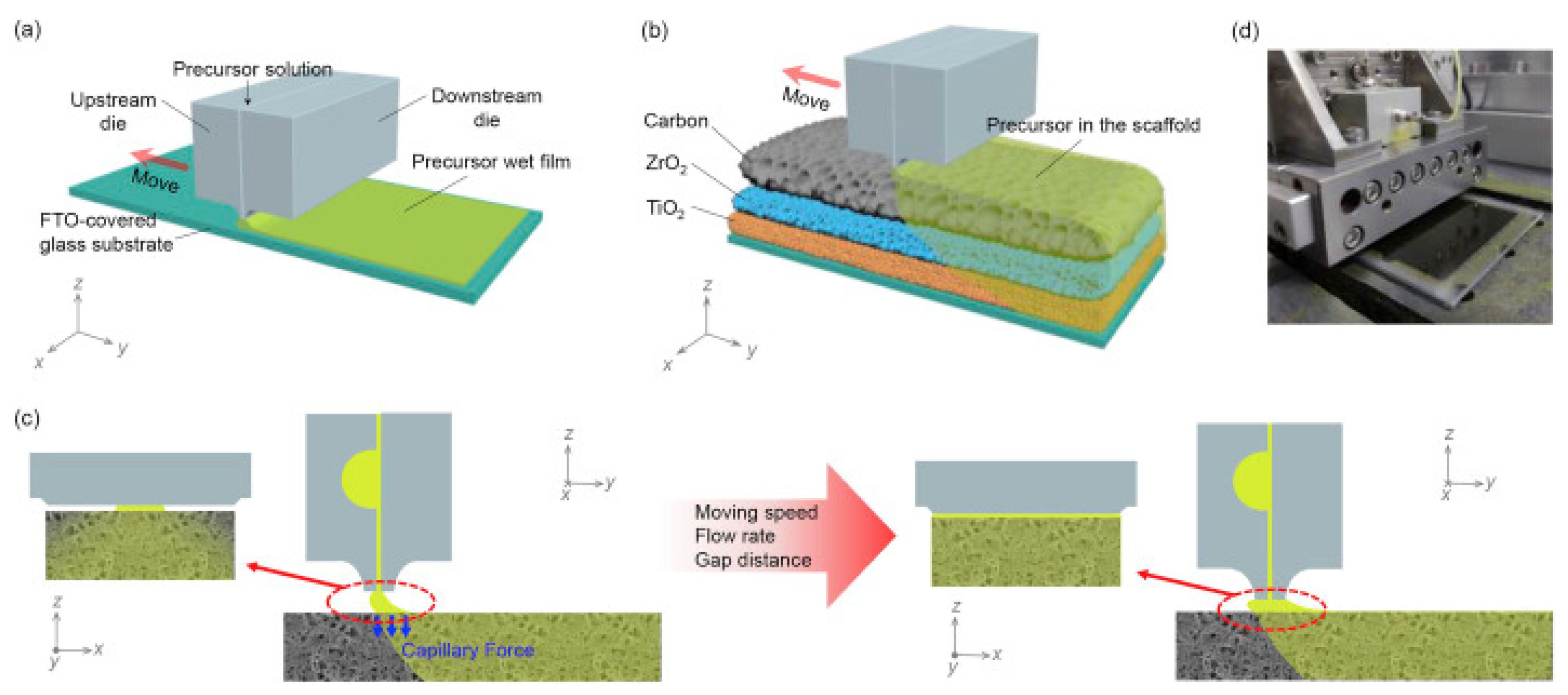
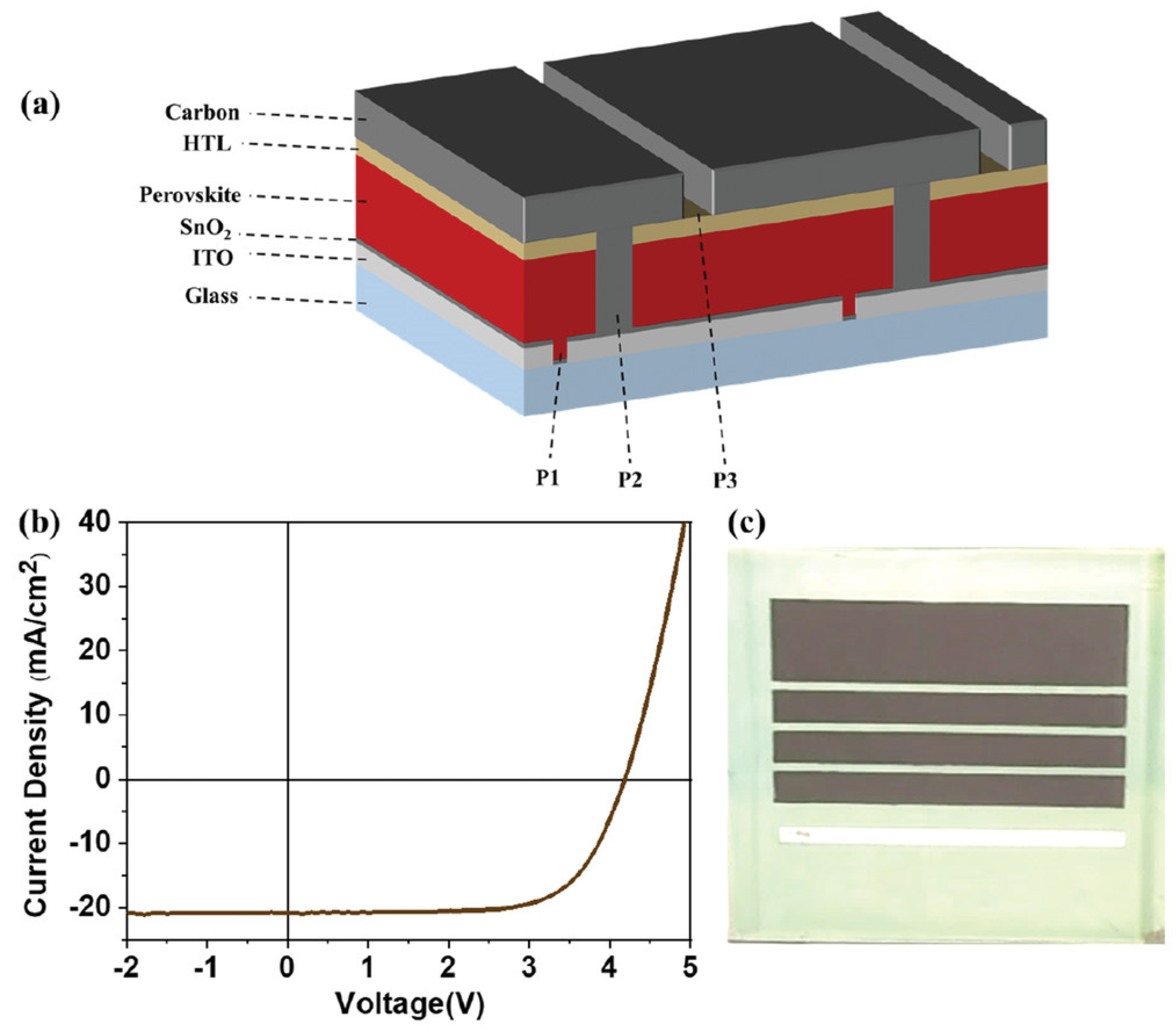
3. Application of C Electrodes in PSCs
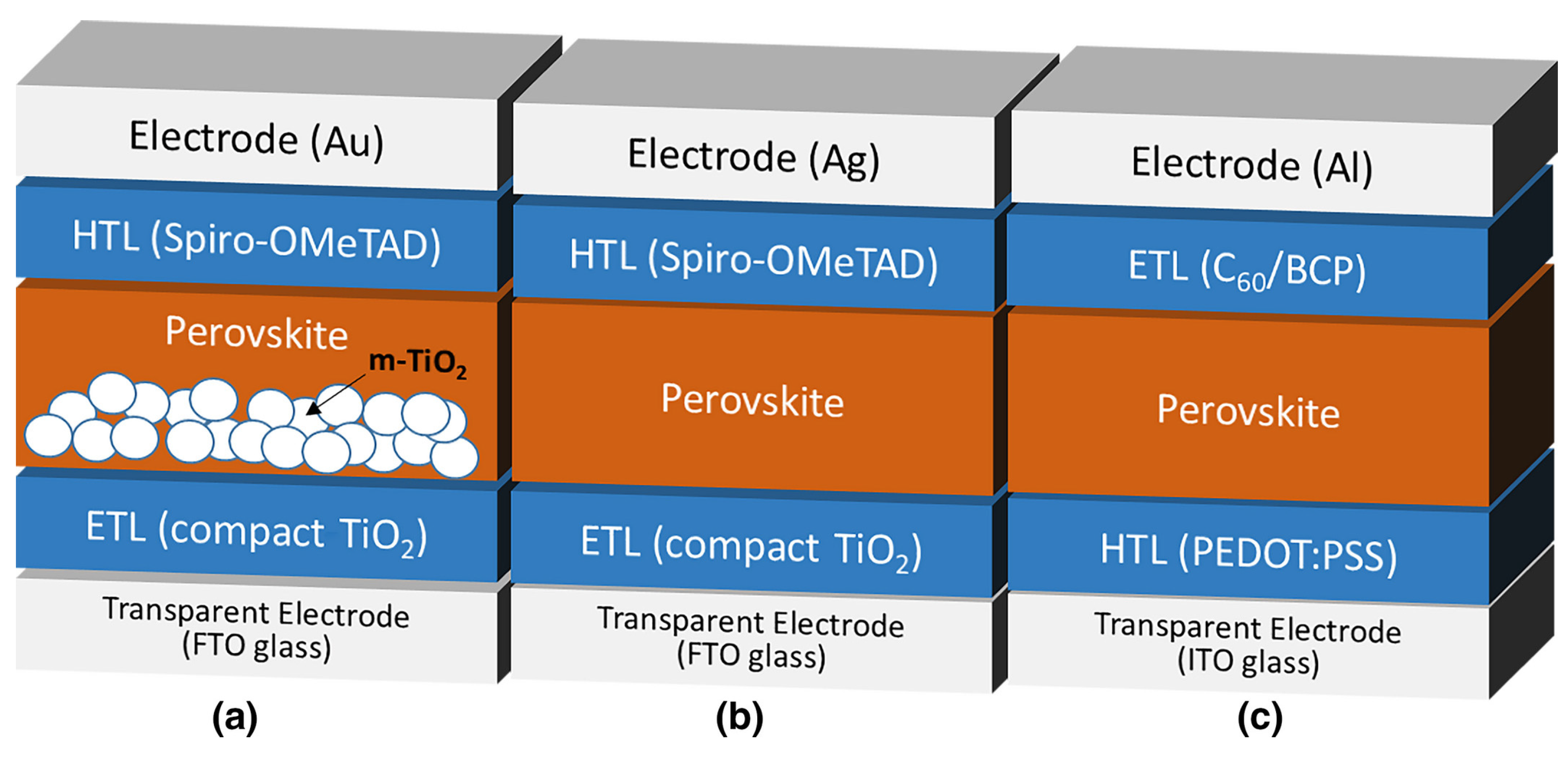
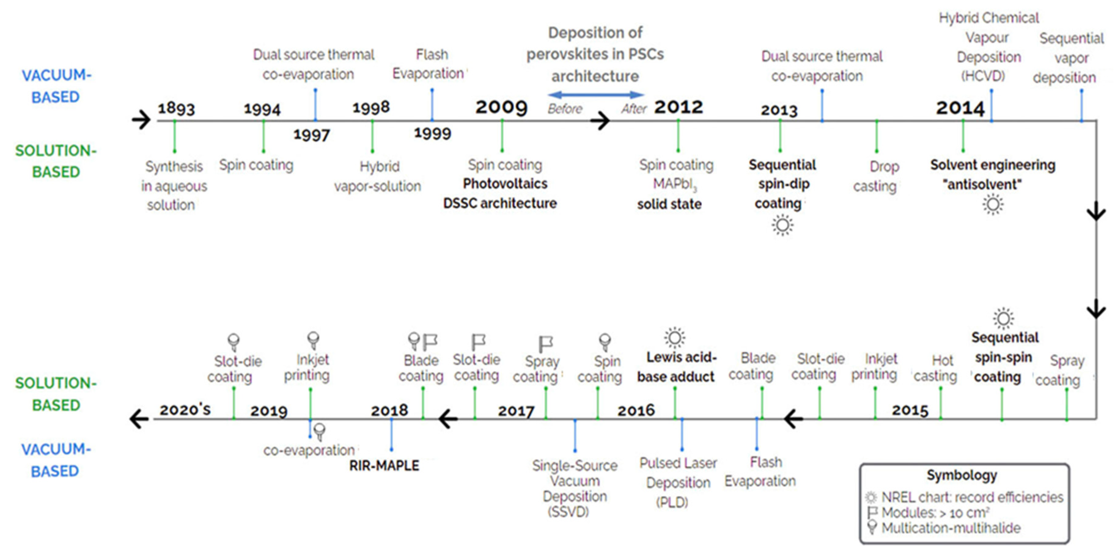
3.1. Perovskite Solar Cells (PSCs)
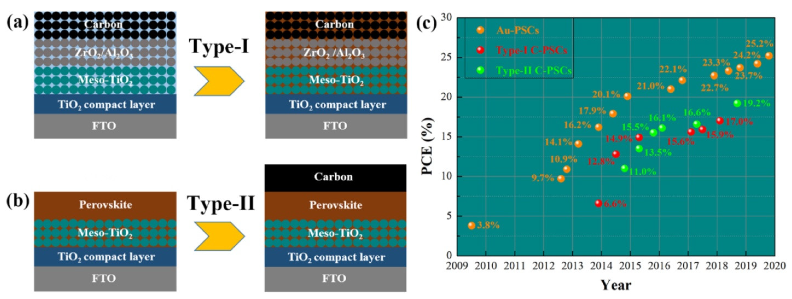
3.2. Carbon-Based Perovskite Solar Cells (C-PSCs)

| C Electrode Type | C Electrode Deposition Method | Perovskite | Hole Transport Material (HTM) | PCE | PCE Stability | Year | Ref. |
|---|---|---|---|---|---|---|---|
| C film prepared from LT C paste | Press transfer | (FA1−xMAx)PbI3-xBrx | Spiro-OMeTAD | 20.04 | 94% after 1000 h ambient air storage | 2022 | [57] |
| Self-adhesive C film prepared from LT C paste | Press transfer | Cs0.05(FA1−xMAx)0.95PbI3-xBrx | Spiro-OMeTAD | 19.2 | 95% retained after 1000 h ambient air storage under atmosphere/94% retained after 80 h under 1 sun equivalent white-light-emitting diode (LED) illumination and maximum power point (MPP) in N2 atmosphere | 2018 | [58] |
| C layer sprayed onto FTO substrate | Press transfer | Cs0.05(FA1−xMAx)0.95PbI3-xBrx | Spiro-OMeTAD | 18.65 | 90% retained after 1000 h at 85°, in the dark | 2019 | [59] |
| LT paste on graphite paper | Press transfer | Cs0.05(MA0.15FA0.85)0.95PbI2.55Br0.45 | Spiro-OMeTAD | 18.56 | 90.5% retained after 1500 h ambient air storage | 2020 | [60] |
| LT paste | Blade coating | 2D Octylammonium Iodide on top of 3D FAPbI3 | - | 18.5 | 82% retained after 500 h of 1 sun illumination | 2022 | [61] |
| LT paste | Doctor blading | FA0.3MA0.7PbI3 | P3HT | 18.22 | 1680 h ambient air storage/retention of ~89% after 600 h under 1 sun illumination in N2 environment | 2019 | [62] |
| LT paste | Doctor blading | (FA0.83MA0.17)PbI2.15Br0.85 | CuSCN | 18.1 | ≈95% after >2000 h under 1 sun illumination | 2019 | [63] |
| LT paste | Doctor blading | GAxMA1−xPbI3 | P3HT + Ta-Wox | 18.1 | 100% after 5000 h in a humid atmosphere | 2021 | [64] |
| LT paste | Doctor blading | Cs0.05(MA0.17FA0.83)0.95Pb(I0.83Br0.17)3 | CuPc | 17.78 | ~100% retained 1200 h ambient air storage | 2019 | [65] |
| LT paste | Doctor blading | FAPbI3 | Cu2ZnSnS4 | 17.71 | 30 days storage | 2020 | [66] |
| LT paste | Doctor blading | Cs0.05(FA0.83MA0.17)0.95Pb(I0.83Br0.17)3 | CuSCN | 17.58 | 80% after 1000 h 1 sun illumination | 2019 | [67] |
| HT paste | Screen printing | Cs0.04(FA1−xMAx)0.96PbI3-xClx | - | 17.47 | 95% of the initial PCE after 1000 h ambient air storage | 2021 | [68] |
| LT paste | Doctor blading | Cs0.05(MA0.17FA0.83)0.95Pb(I0.83Br0.17)3 | CuPc | 17.46 | 97% retained after 1200 h in ambient air storage | 2018 | [69] |
| HT paste | Doctor blading | Cs0.05(MA0.6FA0.4)0.95PbI2.8Br0.2 | NiO | 17.02 | 91% retained after 1000 h at 85°, in the dark | 2017 | [70] |
| HT paste | Screen printing | (5-AVA)xMA1−xPbI3 | - | 16.51 | 91.7% after 1000 h continuous operation at the maximum power point under 1 sun illumination | 2020 | [71] |
| HT paste | Screen printing | Cs0.1Rb0.05FA0.85PbI3 | - | 16.26 | 360 h ambient air storage | 2020 | [72] |
| LT paste | Doctor blading | FAxMA1−xPbIyBr3-y (MWCNTs added) | - | 16.25 | 93% under ambient air conditions for 22 weeks/92.7% retained after200 h heating | 2019 | [73] |
| LT paste | Doctor blading | CH3NH3PbI3 | P3HT | 16.05 | 90% after 1200 h upon ambient air exposure | 2021 | [74] |
| HT paste | Screen printing | CH3NH3PbI3(SrCl2)x | - | 15.9 | ≈90% after 1000 h at 1 sun illumination | 2017 | [75] |
| HT paste | Screen printing | CH3NH3PbI3 | - | 15.89 | ~100% retained after 35 h ambient storage | 2019 | [76] |
| HT paste | Screen printing | (5-AVA)xMA1−xPbI3 | - | 15.77 | N/A | 2019 | [77] |
| HT paste | Screen printing | (5-AVA)xMA1−xPbI3 | - | 15.7 | 500 h under illumination, 2000 h in the dark | 2018 | [78] |
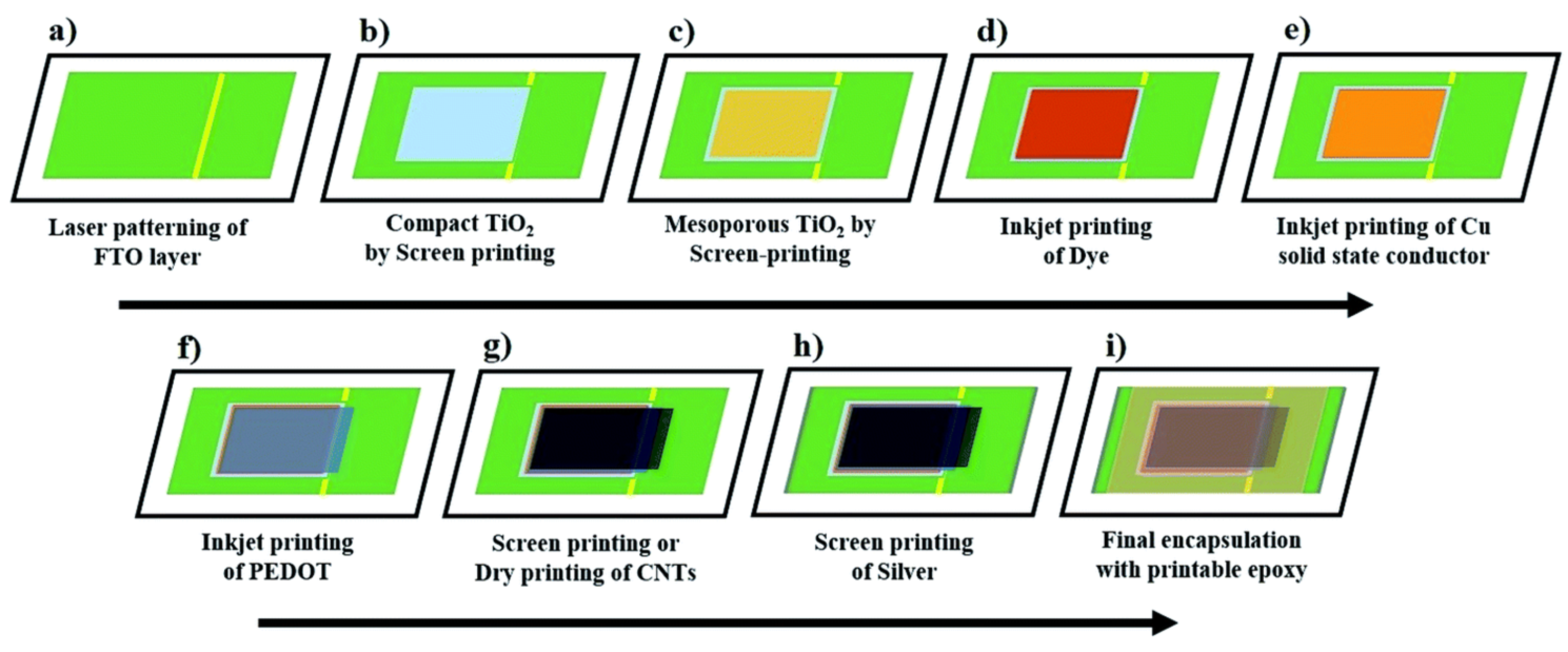
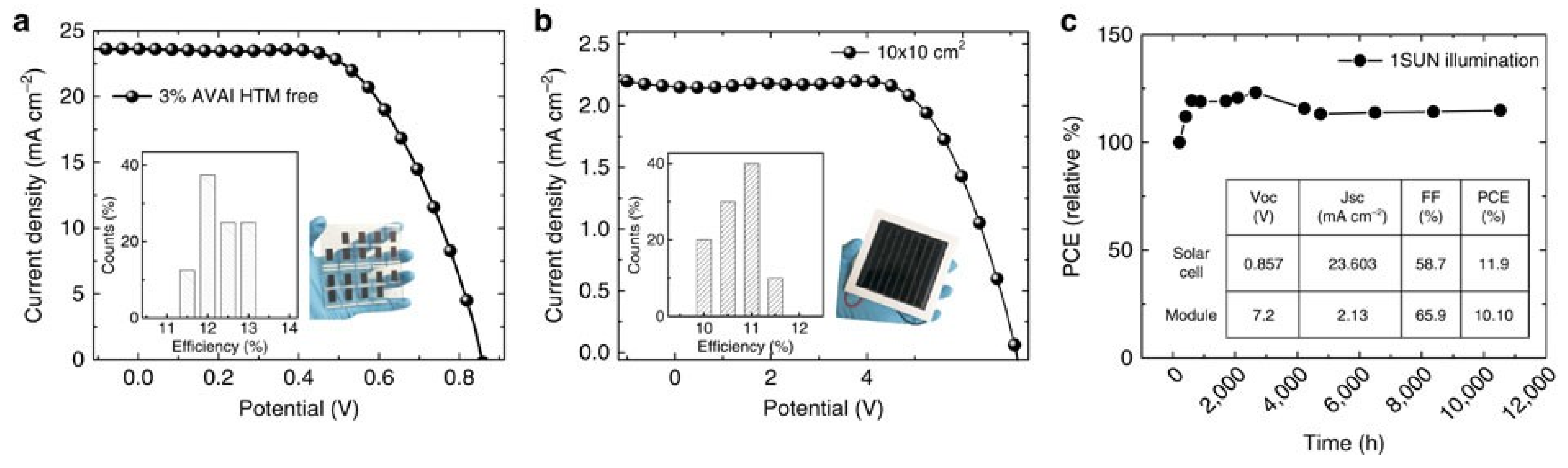
4. Transfer to the Large Area
- >14,000 cm2: large module
- 6500–14,000 cm2: standard module
- 800–6500 cm2: small module
- 200–800 cm2: mini-module
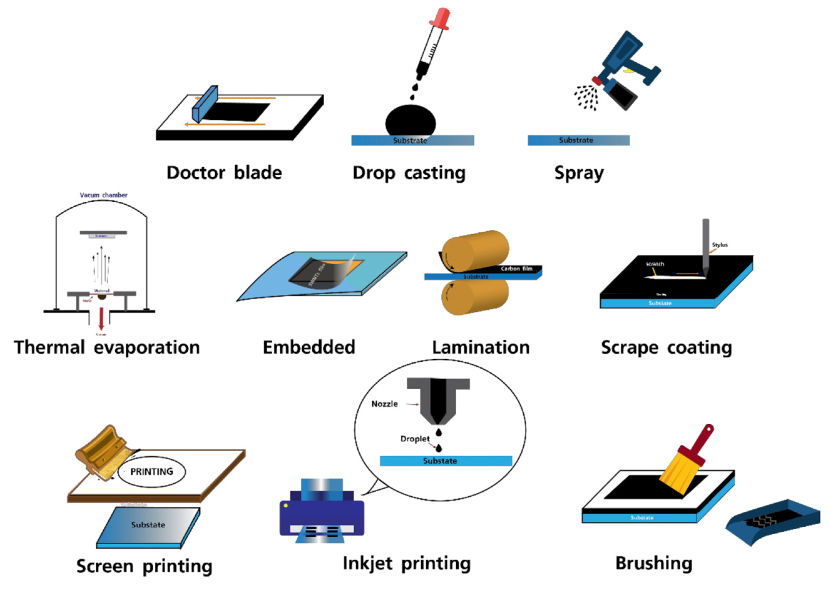
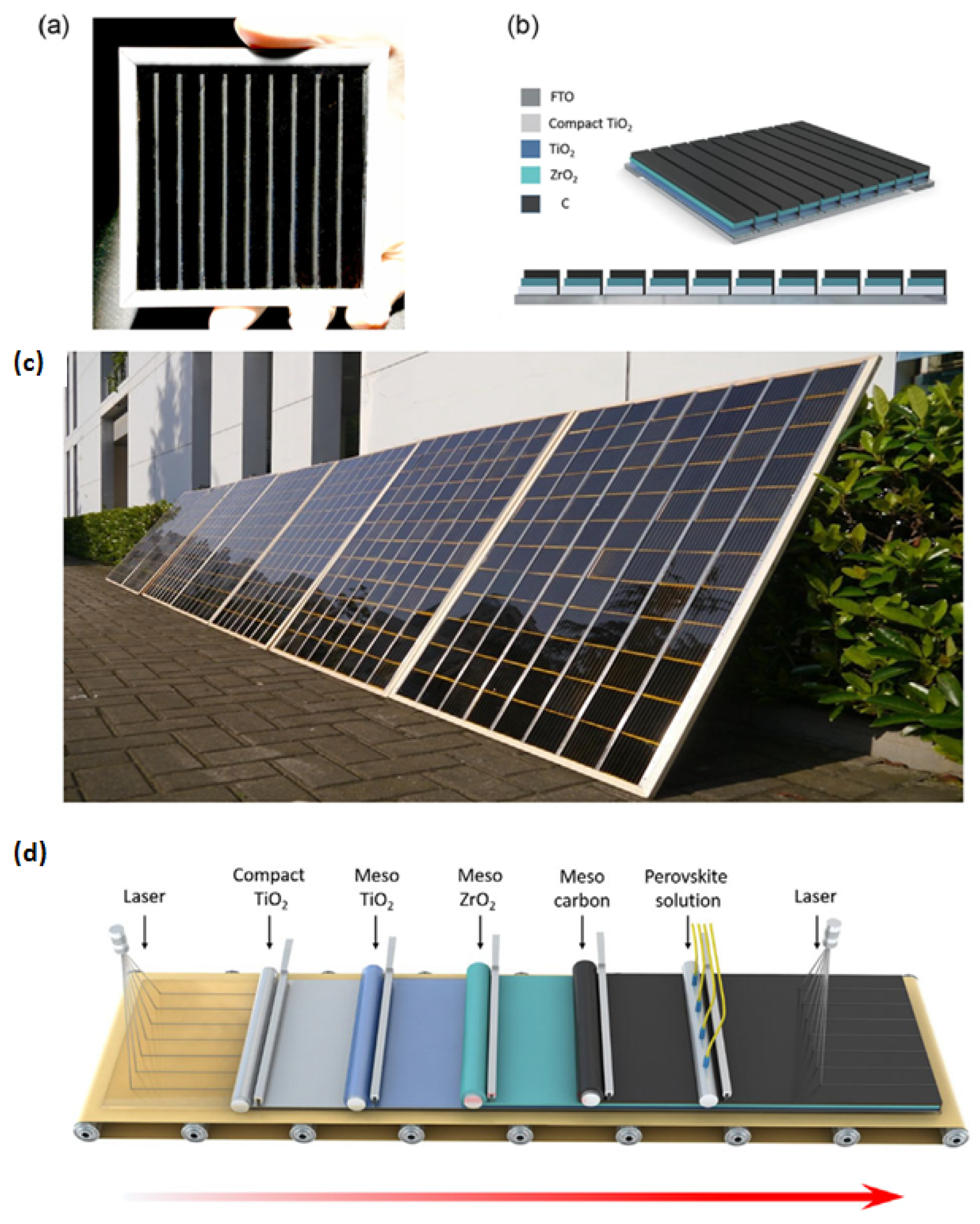
4.1. Large-Area C-PSC Fabrication Technologies
- Solution processing
- Spin coating
- Blade coating
- Slot-die coating
- Spray coating
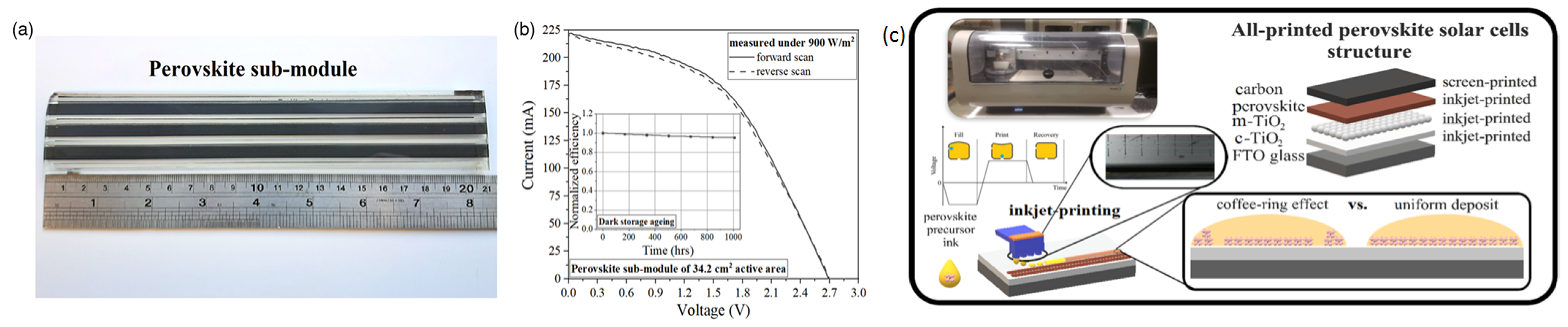
- Inkjet printing
- Screen printing
- Vapor deposition
- Vacuum thermal evaporation
- Chemical vapor deposition
- Flash evaporation
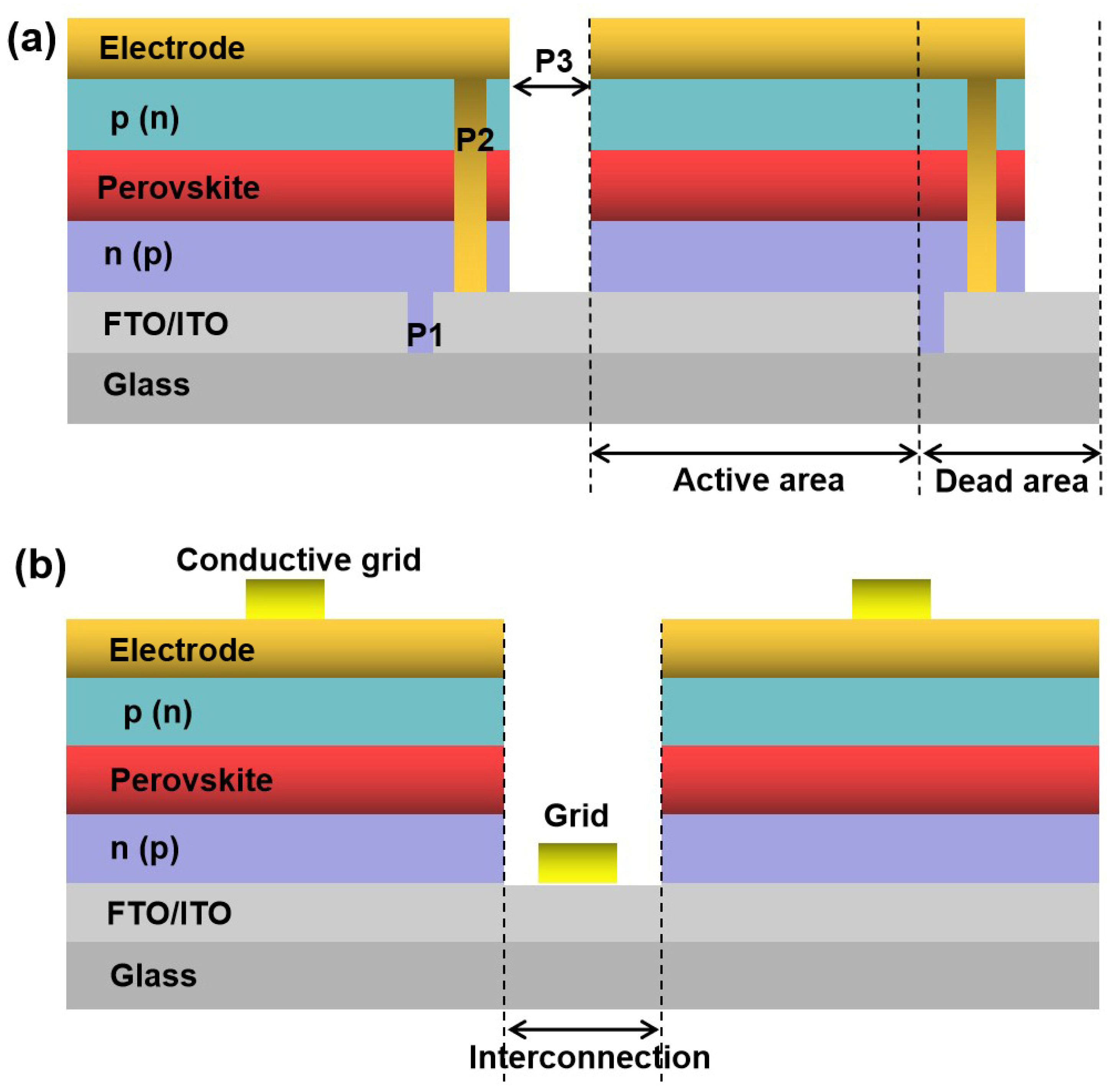
4.2. Interconnection Methods
4.3. Current Status—State of the Art
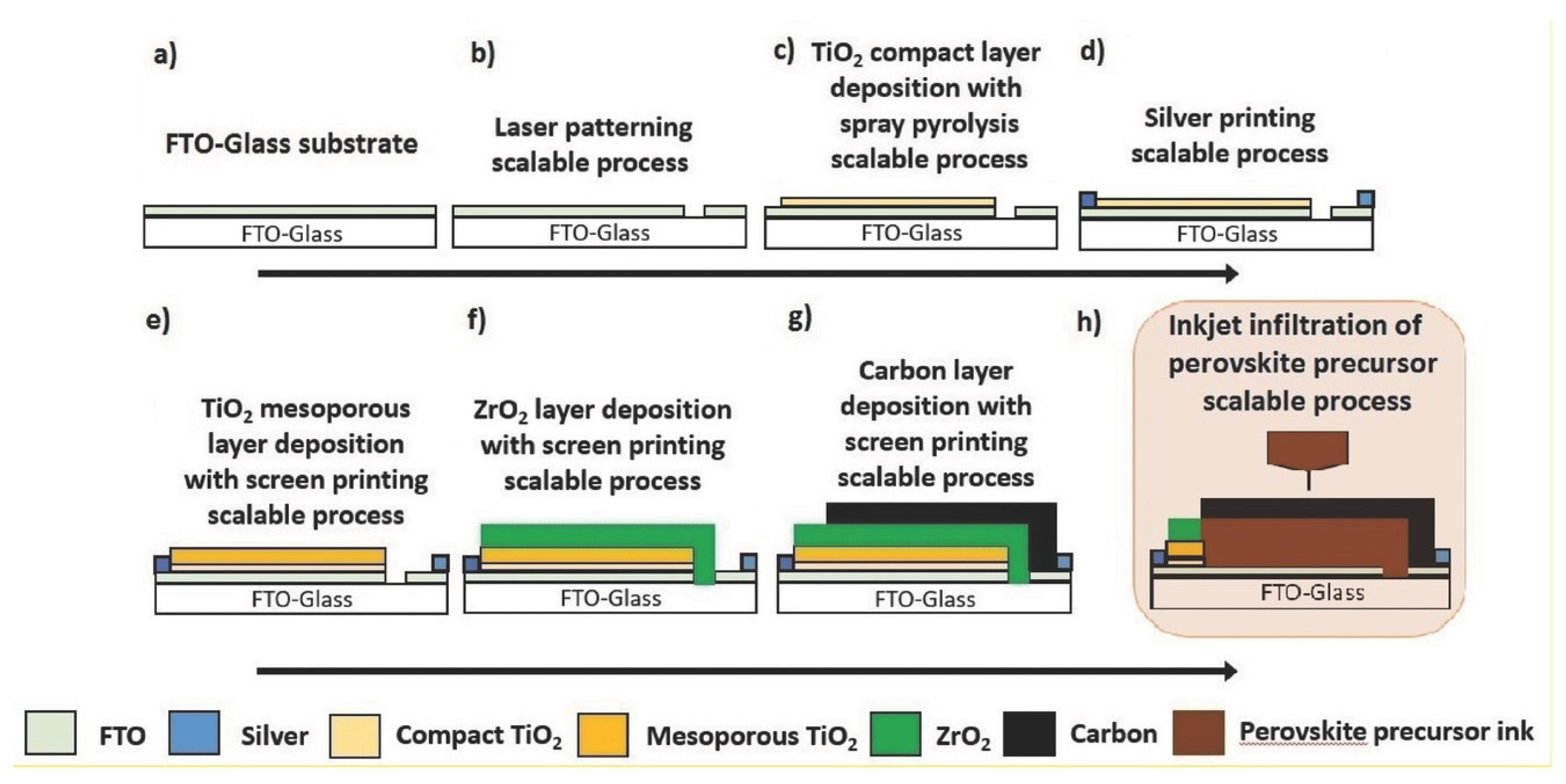
4.3.1. Fully Printable HT-CPSMs
4.3.2. C Electrode Optimization
4.3.3. Device Optimization
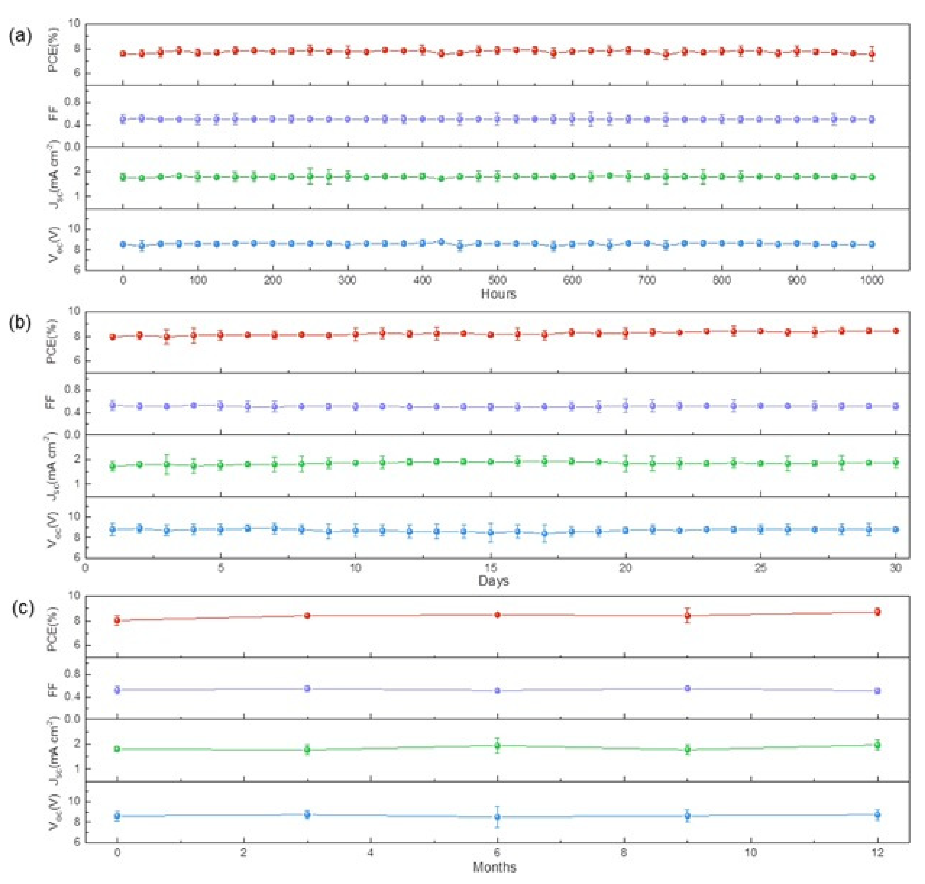
4.3.4. Stability
4.3.5. LT-CPSMs
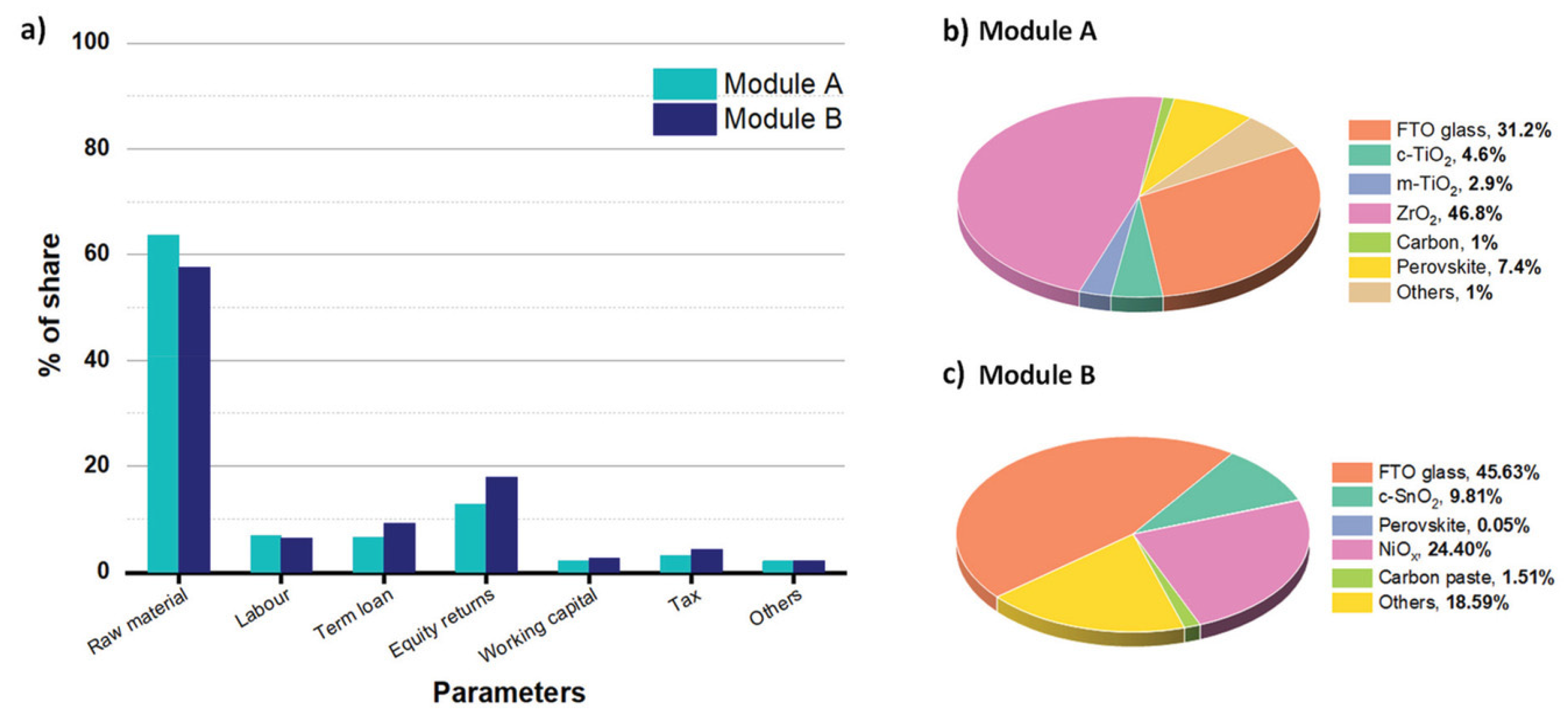
4.4. Cost Analysis
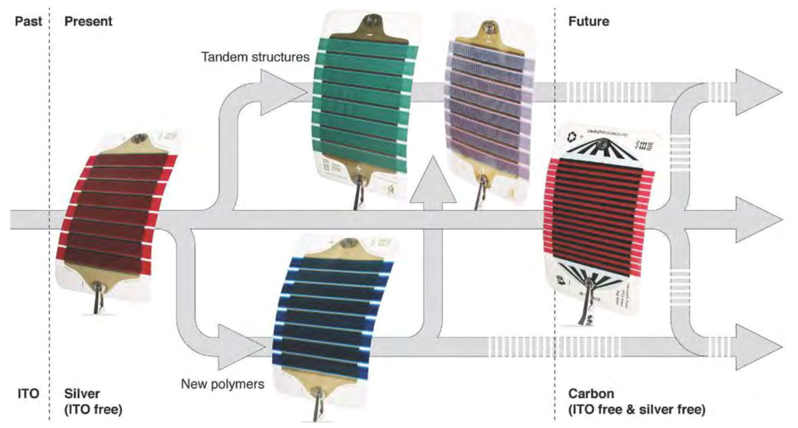
5. Challenges and Future Prospects
6. Conclusions
Funding
Conflicts of Interest
Abbreviations
| 5-AVAI | 5-Ammonium valeric acid iodide |
| Ag | Silver (element) |
| Al | Aluminium (element) |
| Al2O3 | Aluminium oxide |
| A.M. | Air Mass |
| Au | Gold (element) |
| BHJ | Bulk HeteroJunction |
| C | Carbon (element) |
| C-PSC | Carbon Perovskite Solar Cell |
| C-PSM | Carbon Perovskite Solar Module |
| CB | Carbon black |
| CdSe | Cadmium Selenide |
| CE | Counter Electrode |
| CNH | Carbon nanohorn |
| CNF | Carbon nanotube fibre |
| CNT | Carbon nanotube |
| Co | Cobalt (element) |
| CsBr | Caesium Bromide |
| CsCl | Caesium Chloride |
| CsI | Caesium Iodide |
| CTL | Charge Transport Layer |
| Cu | Copper (element) |
| CuPc | Copper phthalocyanine |
| CuSCN | Copper(I) thiocyanate |
| DMF | Dimethylformamide |
| DSSC | Dye Sensitized Solar Cell |
| EIS | Electrochemical Impedance Spectroscopy |
| ETL | Electron Transport Layer |
| FA | Formamide |
| FAI | Formamidinium Iodide |
| FF | Fill Factor |
| FTO | Fluorine-doped Tin Oxide |
| HOIP | Hybrid Organic Inorganic Perovskite |
| HT | High Temperature |
| HT-CPSC | High Temperature Carbon Perovskite Solar Cell |
| HTL | Hole Transport Layer |
| HTM | Hole Transport Material |
| In | Indium (element) |
| Jsc | Short Circuit Current Density |
| LCOE | Levelized Cost of Energy |
| LT | Low Temperature |
| LT-CPSC | Low Temperature Carbon Perovskite Solar Cell |
| MA | Methylamine |
| MAI | Methylammonium Iodide |
| MC | Mesoporous Carbon |
| NiO | Nickel Oxide |
| NREL | National Renewable Energy Laboratory |
| OPV | Organic Photovoltaic |
| OSC | Organic Solar Cell |
| P3HT | poly(3-hexylthiophene-2,5-diyl) |
| Pb | Lead (element) |
| PCE | Power Conversion Efficiency |
| PHJ | Planar HeteroJunction |
| Pm | Maximum Power |
| PSC | Perovskite Solar Cell |
| PSM | Perovskite Solar Module |
| Pt | Platinum (element) |
| PV | Photovoltaic |
| QD | Quantum Dot |
| QD-SSC | Quantum Dot Sensitized Solar Cell |
| RH | Relative Humidity |
| Se | Selenium (element) |
| SEM | Scanning Electron Microscopy |
| Spiro-OMeTAD | 2,2′,7,7′-Tetrakis[N,N-di(4-methoxyphenyl)amino]-9,9’-spirobifluorene |
| SWCNH | Single Wall Carbon Nanohorn |
| SWCNT | Single Wall Carbon Nanotube |
| TCO | Transparent Conductive Oxide |
| TEM | Transmission Electron Microscopy |
| Ti | Titanium (element) |
| TiO2 | Titanium Dioxide |
| UV | Ultraviolet |
| US | United States |
| Voc | Open Circuit Voltage |
| Zn | Zinc (element) |
| ZrO2 | Zirconium Dioxide |
References
- Kojima, A.; Teshima, K.; Shirai, Y.; Miyasaka, T. Organometal Halide Perovskites as Visible-Light Sensitizers for Photovoltaic Cells. J. Am. Chem. Soc. 2009, 131, 6050–6051. [Google Scholar] [CrossRef] [PubMed]
- NREL Module Efficiency Chart. Available online: https://www.nrel.gov/pv/module-efficiency.html (accessed on 10 December 2022).
- O’Regan, B.; Grätzel, M. A Low-Cost, High-Efficiency Solar Cell Based on Dye-Sensitized Colloidal TiO2 Films. Nature 1991, 353, 737–740. [Google Scholar] [CrossRef]
- NREL Efficiency Chart. Available online: https://www.nrel.gov/pv/cell-efficiency.html (accessed on 10 December 2022).
- Michaels, H.; Rinderle, M.; Freitag, R.; Benesperi, I.; Edvinsson, T.; Socher, R.; Gagliardi, A.; Freitag, M. Dye-Sensitized Solar Cells under Ambient Light Powering Machine Learning: Towards Autonomous Smart Sensors for the Internet of Things. Chem. Sci. 2020, 11, 2895–2906. [Google Scholar] [CrossRef] [PubMed] [Green Version]
- Parisi, M.L.; Maranghi, S.; Basosi, R. The Evolution of the Dye Sensitized Solar Cells from Grätzel Prototype to Up-Scaled Solar Applications: A Life Cycle Assessment Approach. Renew. Sustain. Energy Rev. 2014, 39, 124–138. [Google Scholar] [CrossRef]
- Samantaray, M.R.; Mondal, A.K.; Murugadoss, G.; Pitchaimuthu, S.; Das, S.; Bahru, R.; Mohamed, M.A. Synergetic Effects of Hybrid Carbon Nanostructured Counter Electrodes for Dye-Sensitized Solar Cells: A Review. Materials 2020, 13, 2779. [Google Scholar] [CrossRef]
- Wu, C.-S.; Chang, T.-W.; Teng, H.; Lee, Y.-L. High Performance Carbon Black Counter Electrodes for Dye-Sensitized Solar Cells. Energy 2016, 115, 513–518. [Google Scholar] [CrossRef]
- Monreal-Bernal, A.; Bidikoudi, M.; Costa, R.D. Carbon Nanotubes in Hybrid Photovoltaics: Dye Sensitized and Perovskites Solar Cells. In Carbon Based Nanomaterials for Advanced Thermal and Electrochemical Energy Storage and Conversion; Elsevier: Amsterdam, The Netherlands, 2019; pp. 201–248. ISBN 978-0-12-814083-3. [Google Scholar]
- Kim, J.H.; Hong, S.K.; Yoo, S.-J.; Woo, C.Y.; Choi, J.W.; Lee, D.; Kang, J.-W.; Lee, H.W.; Song, M. Pt-Free, Cost-Effective and Efficient Counter Electrode with Carbon Nanotube Yarn for Solid-State Fiber Dye-Sensitized Solar Cells. Dye. Pigm. 2021, 185, 108855. [Google Scholar] [CrossRef]
- Zhang, J.; Wang, Z.; Li, X.; Yang, J.; Song, C.; Li, Y.; Cheng, J.; Guan, Q.; Wang, B. Flexible Platinum-Free Fiber-Shaped Dye Sensitized Solar Cell with 10.28% Efficiency. ACS Appl. Energy Mater. 2019, 2, 2870–2877. [Google Scholar] [CrossRef]
- Lodermeyer, F.; Costa, R.D.; Guldi, D.M. Implementation of Single-Walled Carbon Nanohorns into Solar Cell Schemes. Adv. Energy Mater. 2017, 7, 1601883. [Google Scholar] [CrossRef]
- Carli, S.; Casarin, L.; Syrgiannis, Z.; Boaretto, R.; Benazzi, E.; Caramori, S.; Prato, M.; Bignozzi, C.A. Single Walled Carbon Nanohorns as Catalytic Counter Electrodes for Co(III)/(II) Electron Mediators in Dye Sensitized Cells. ACS Appl. Mater. Interfaces 2016, 8, 14604–14612. [Google Scholar] [CrossRef]
- Chen, M.; Shao, L.-L.; Qian, X.; Liu, L.; Ren, T.-Z.; Yuan, Z.-Y. Mesoporous Carbon Counter Electrode Materials for Dye-Sensitized Solar Cells: The Effect of Structural Mesopore Ordering. Chem. Eng. J. 2014, 256, 23–31. [Google Scholar] [CrossRef]
- Kakiage, K.; Aoyama, Y.; Yano, T.; Oya, K.; Fujisawa, J.; Hanaya, M. Highly-Efficient Dye-Sensitized Solar Cells with Collaborative Sensitization by Silyl-Anchor and Carboxy-Anchor Dyes. Chem. Commun. 2015, 51, 15894–15897. [Google Scholar] [CrossRef] [PubMed]
- Kay, A.; Grätzel, M. Low Cost Photovoltaic Modules Based on Dye Sensitized Nanocrystalline Titanium Dioxide and Carbon Powder. Sol. Energy Mater. Sol. Cells 1996, 44, 99–117. [Google Scholar] [CrossRef]
- Murakami, T.N.; Ito, S.; Wang, Q.; Nazeeruddin, M.K.; Bessho, T.; Cesar, I.; Liska, P.; Humphry-Baker, R.; Comte, P.; Péchy, P.; et al. Highly Efficient Dye-Sensitized Solar Cells Based on Carbon Black Counter Electrodes. J. Electrochem. Soc. 2006, 153, A2255. [Google Scholar] [CrossRef]
- Zhao, B.; Huang, H.; Jiang, P.; Zhao, H.; Huang, X.; Shen, P.; Wu, D.; Fu, R.; Tan, S. Flexible Counter Electrodes Based on Mesoporous Carbon Aerogel for High-Performance Dye-Sensitized Solar Cells. J. Phys. Chem. C 2011, 115, 22615–22621. [Google Scholar] [CrossRef]
- Monreal-Bernal, A.; Vilatela, J.J.; Costa, R.D. CNT Fibres as Dual Counter-Electrode/Current-Collector in Highly Efficient and Stable Dye-Sensitized Solar Cells. Carbon 2019, 141, 488–496. [Google Scholar] [CrossRef]
- Wu, K.-L.; Huckaba, A.J.; Clifford, J.N.; Yang, Y.-W.; Yella, A.; Palomares, E.; Grätzel, M.; Chi, Y.; Nazeeruddin, M.K. Molecularly Engineered Ru(II) Sensitizers Compatible with Cobalt(II/III) Redox Mediators for Dye-Sensitized Solar Cells. Inorg. Chem. 2016, 55, 7388–7395. [Google Scholar] [CrossRef]
- Ju, M.J.; Choi, I.T.; Zhong, M.; Lim, K.; Ko, J.; Mohin, J.; Lamson, M.; Kowalewski, T.; Matyjaszewski, K.; Kim, H.K. Copolymer-Templated Nitrogen-Enriched Nanocarbons as a Low Charge-Transfer Resistance and Highly Stable Alternative to Platinum Cathodes in Dye-Sensitized Solar Cells. J. Mater. Chem. A 2015, 3, 4413–4419. [Google Scholar] [CrossRef]
- Zhu, Y.; Guo, H.; Zheng, H.; Lin, Y.; Gao, C.; Han, Q.; Wu, M. Choose a Reasonable Counter Electrode Catalyst toward a Fixed Redox Couple in Dye-Sensitized Solar Cells. Nano Energy 2016, 21, 1–18. [Google Scholar] [CrossRef]
- Kim, C.K.; Choi, I.T.; Kang, S.H.; Kim, H.K. Anchovy-Derived Nitrogen and Sulfur Co-Doped Porous Carbon Materials for High-Performance Supercapacitors and Dye-Sensitized Solar Cells. RSC Adv. 2017, 7, 35565–35574. [Google Scholar] [CrossRef] [Green Version]
- Hashmi, S.G.; Sonai, G.G.; Iftikhar, H.; Lund, P.D.; Nogueira, A.F. Printed Single-Walled Carbon-Nanotubes-Based Counter Electrodes for Dye-Sensitized Solar Cells with Copper-Based Redox Mediators. Semicond. Sci. Technol. 2019, 34, 105001. [Google Scholar] [CrossRef]
- Kokkonen, M.; Talebi, P.; Zhou, J.; Asgari, S.; Soomro, S.A.; Elsehrawy, F.; Halme, J.; Ahmad, S.; Hagfeldt, A.; Hashmi, S.G. Advanced Research Trends in Dye-Sensitized Solar Cells. J. Mater. Chem. A 2021, 9, 10527–10545. [Google Scholar] [CrossRef] [PubMed]
- Nozik, A.J.; Beard, M.C.; Luther, J.M.; Law, M.; Ellingson, R.J.; Johnson, J.C. Semiconductor Quantum Dots and Quantum Dot Arrays and Applications of Multiple Exciton Generation to Third-Generation Photovoltaic Solar Cells. Chem. Rev. 2010, 110, 6873–6890. [Google Scholar] [CrossRef] [PubMed]
- Semonin, O.E.; Luther, J.M.; Choi, S.; Chen, H.-Y.; Gao, J.; Nozik, A.J.; Beard, M.C. Peak External Photocurrent Quantum Efficiency Exceeding 100% via MEG in a Quantum Dot Solar Cell. Science 2011, 334, 1530–1533. [Google Scholar] [CrossRef] [PubMed]
- Plass, R.; Pelet, S.; Krueger, J.; Grätzel, M.; Bach, U. Quantum Dot Sensitization of Organic–Inorganic Hybrid Solar Cells. J. Phys. Chem. B 2002, 106, 7578–7580. [Google Scholar] [CrossRef]
- Sahu, A.; Garg, A.; Dixit, A. A Review on Quantum Dot Sensitized Solar Cells: Past, Present and Future towards Carrier Multiplication with a Possibility for Higher Efficiency. Sol. Energy 2020, 203, 210–239. [Google Scholar] [CrossRef]
- Pan, Z.; Rao, H.; Mora-Seró, I.; Bisquert, J.; Zhong, X. Quantum Dot-Sensitized Solar Cells. Chem. Soc. Rev. 2018, 47, 7659–7702. [Google Scholar] [CrossRef]
- Du, Z.; Pan, Z.; Fabregat-Santiago, F.; Zhao, K.; Long, D.; Zhang, H.; Zhao, Y.; Zhong, X.; Yu, J.-S.; Bisquert, J. Carbon Counter-Electrode-Based Quantum-Dot-Sensitized Solar Cells with Certified Efficiency Exceeding 11%. J. Phys. Chem. Lett. 2016, 7, 3103–3111. [Google Scholar] [CrossRef]
- Du, J.; Du, Z.; Hu, J.-S.; Pan, Z.; Shen, Q.; Sun, J.; Long, D.; Dong, H.; Sun, L.; Zhong, X.; et al. Zn–Cu–In–Se Quantum Dot Solar Cells with a Certified Power Conversion Efficiency of 11.6%. J. Am. Chem. Soc. 2016, 138, 4201–4209. [Google Scholar] [CrossRef]
- Jiao, S.; Du, J.; Du, Z.; Long, D.; Jiang, W.; Pan, Z.; Li, Y.; Zhong, X. Nitrogen-Doped Mesoporous Carbons as Counter Electrodes in Quantum Dot Sensitized Solar Cells with a Conversion Efficiency Exceeding 12%. J. Phys. Chem. Lett. 2017, 8, 559–564. [Google Scholar] [CrossRef]
- Zhang, L.; Pan, Z.; Wang, W.; Du, J.; Ren, Z.; Shen, Q.; Zhong, X. Copper Deficient Zn–Cu–In–Se Quantum Dot Sensitized Solar Cells for High Efficiency. J. Mater. Chem. A 2017, 5, 21442–21451. [Google Scholar] [CrossRef]
- Wang, W.; Feng, W.; Du, J.; Xue, W.; Zhang, L.; Zhao, L.; Li, Y.; Zhong, X. Cosensitized Quantum Dot Solar Cells with Conversion Efficiency over 12%. Adv. Mater. 2018, 30, 1705746. [Google Scholar] [CrossRef] [PubMed]
- Peng, W.; Du, J.; Pan, Z.; Nakazawa, N.; Sun, J.; Du, Z.; Shen, G.; Yu, J.; Hu, J.-S.; Shen, Q.; et al. Alloying Strategy in Cu–In–Ga–Se Quantum Dots for High Efficiency Quantum Dot Sensitized Solar Cells. ACS Appl. Mater. Interfaces 2017, 9, 5328–5336. [Google Scholar] [CrossRef] [PubMed]
- Yilmaz, E.Ç.; Yeşilyurt, M.K.; Öner, İ.V.; Ömeroglu, G.; Özakin, A.N. Operational Stability and Degradation of Organic Solar Cells. Period. Eng. Nat. Sci. 2017, 5, 105. [Google Scholar] [CrossRef] [Green Version]
- Muchuweni, E.; Mombeshora, E.T.; Martincigh, B.S.; Nyamori, V.O. Recent Applications of Carbon Nanotubes in Organic Solar Cells. Front. Chem. 2022, 9, 733552. [Google Scholar] [CrossRef]
- Tang, C.W. Two-layer Organic Photovoltaic Cell. Appl. Phys. Lett. 1986, 48, 183–185. [Google Scholar] [CrossRef]
- Zhu, L.; Zhang, M.; Xu, J.; Li, C.; Yan, J.; Zhou, G.; Zhong, W.; Hao, T.; Song, J.; Xue, X.; et al. Single-Junction Organic Solar Cells with over 19% Efficiency Enabled by a Refined Double-Fibril Network Morphology. Nat. Mater. 2022, 21, 656–663. [Google Scholar] [CrossRef]
- Riede, M.; Spoltore, D.; Leo, K. Organic Solar Cells—The Path to Commercial Success. Adv. Energy Mater. 2021, 11, 2002653. [Google Scholar] [CrossRef]
- Wan, X.; Long, G.; Huang, L.; Chen, Y. Graphene—A Promising Material for Organic Photovoltaic Cells. Adv. Mater. 2011, 23, 5342–5358. [Google Scholar] [CrossRef]
- Jin, S.; Jun, G.H.; Jeon, S.; Hong, S.H. Design and Application of Carbon Nanomaterials for Photoactive and Charge Transport Layers in Organic Solar Cells. Nano Converg. 2016, 3, 8. [Google Scholar] [CrossRef] [Green Version]
- Dos Reis Benatto, G.A.; Roth, B.; Madsen, M.V.; Hösel, M.; Søndergaard, R.R.; Jørgensen, M.; Krebs, F.C. Carbon: The Ultimate Electrode Choice for Widely Distributed Polymer Solar Cells. Adv. Energy Mater. 2014, 4, 1400732. [Google Scholar] [CrossRef]
- Krebs, F.C.; Hösel, M.; Corazza, M.; Roth, B.; Madsen, M.V.; Gevorgyan, S.A.; Søndergaard, R.R.; Karg, D.; Jørgensen, M. Freely Available OPV—The Fast Way to Progress. Energy Technol. 2013, 1, 378–381. [Google Scholar] [CrossRef]
- Perulli, A.; Lattante, S.; Persano, A.; Cola, A.; Anni, M. On the Homogeneity of the External Quantum Efficiency in a Free OPV Roll-to-Roll Flexible Solar Module. Synth. Met. 2019, 247, 248–254. [Google Scholar] [CrossRef]
- Mitzi, D.B. Synthesis, Structure, and Properties of Organic-Inorganic Perovskites and Related Materials. In Progress in Inorganic Chemistry; John Wiley & Sons, Ltd.: Hoboken, NJ, USA, 1999; pp. 1–121. ISBN 978-0-470-16649-9. [Google Scholar]
- Min, H.; Lee, D.Y.; Kim, J.; Kim, G.; Lee, K.S.; Kim, J.; Paik, M.J.; Kim, Y.K.; Kim, K.S.; Kim, M.G.; et al. Perovskite Solar Cells with Atomically Coherent Interlayers on SnO2 Electrodes. Nature 2021, 598, 444–450. [Google Scholar] [CrossRef]
- Ferguson, V.; Silva, S.R.P.; Zhang, W. Carbon Materials in Perovskite Solar Cells: Prospects and Future Challenges. Energy Environ. Mater. 2019, 2, 107–118. [Google Scholar] [CrossRef] [Green Version]
- Zhao, L.; Kerner, R.A.; Xiao, Z.; Lin, Y.L.; Lee, K.M.; Schwartz, J.; Rand, B.P. Redox Chemistry Dominates the Degradation and Decomposition of Metal Halide Perovskite Optoelectronic Devices. ACS Energy Lett. 2016, 1, 595–602. [Google Scholar] [CrossRef]
- Svanström, S.; Jacobsson, T.J.; Boschloo, G.; Johansson, E.M.J.; Rensmo, H.; Cappel, U.B. Degradation Mechanism of Silver Metal Deposited on Lead Halide Perovskites. ACS Appl. Mater. Interfaces 2020, 12, 7212–7221. [Google Scholar] [CrossRef] [Green Version]
- Domanski, K.; Correa-Baena, J.-P.; Mine, N.; Nazeeruddin, M.K.; Abate, A.; Saliba, M.; Tress, W.; Hagfeldt, A.; Grätzel, M. Not All That Glitters Is Gold: Metal-Migration-Induced Degradation in Perovskite Solar Cells. ACS Nano 2016, 10, 6306–6314. [Google Scholar] [CrossRef]
- Cai, Y.; Liang, L.; Gao, P. Promise of Commercialization: Carbon Materials for Low-Cost Perovskite Solar Cells. Chin. Phys. B 2018, 27, 018805. [Google Scholar] [CrossRef] [Green Version]
- Ku, Z.; Rong, Y.; Xu, M.; Liu, T.; Han, H. Full Printable Processed Mesoscopic CH3NH3PbI3/TiO2 Heterojunction Solar Cells with Carbon Counter Electrode. Sci. Rep. 2013, 3, 3132. [Google Scholar] [CrossRef] [Green Version]
- Zhang, H.; Song, K.; Zhu, L.; Meng, Q. Back-Interface Regulation for Carbon-Based Perovskite Solar Cells. Carbon 2020, 168, 372–391. [Google Scholar] [CrossRef]
- Bogachuk, D.; Yang, B.; Suo, J.; Martineau, D.; Verma, A.; Narbey, S.; Anaya, M.; Frohna, K.; Doherty, T.; Müller, D.; et al. Perovskite Solar Cells with Carbon-Based Electrodes—Quantification of Losses and Strategies to Overcome Them. Adv. Energy Mater. 2022, 12, 2103128. [Google Scholar] [CrossRef]
- Zhang, H.; Li, Y.; Tan, S.; Chen, Z.; Song, K.; Huang, S.; Shi, J.; Luo, Y.; Li, D.; Meng, Q. High-Efficiency (>20%) Planar Carbon-Based Perovskite Solar Cells through Device Configuration Engineering. J. Colloid Interface Sci. 2022, 608, 3151–3158. [Google Scholar] [CrossRef]
- Zhang, H.; Xiao, J.; Shi, J.; Su, H.; Luo, Y.; Li, D.; Wu, H.; Cheng, Y.-B.; Meng, Q. Self-Adhesive Macroporous Carbon Electrodes for Efficient and Stable Perovskite Solar Cells. Adv. Funct. Mater. 2018, 28, 1802985. [Google Scholar] [CrossRef]
- Zhang, C.; Wang, S.; Zhang, H.; Feng, Y.; Tian, W.; Yan, Y.; Bian, J.; Wang, Y.; Jin, S.; Zakeeruddin, S.M.; et al. Efficient Stable Graphene-Based Perovskite Solar Cells with High Flexibility in Device Assembling via Modular Architecture Design. Energy Environ. Sci. 2019, 12, 3585–3594. [Google Scholar] [CrossRef]
- Su, H.; Xiao, J.; Li, Q.; Peng, C.; Zhang, X.; Mao, C.; Yao, Q.; Lu, Y.; Ku, Z.; Zhong, J.; et al. Carbon Film Electrode Based Square-Centimeter Scale Planar Perovskite Solar Cells Exceeding 17% Efficiency. Mater. Sci. Semicond. Process. 2020, 107, 104809. [Google Scholar] [CrossRef]
- Zouhair, S.; Yoo, S.-M.; Bogachuk, D.; Herterich, J.P.; Lim, J.; Kanda, H.; Son, B.; Yun, H.J.; Würfel, U.; Chahboun, A.; et al. Employing 2D-Perovskite as an Electron Blocking Layer in Highly Efficient (18.5%) Perovskite Solar Cells with Printable Low Temperature Carbon Electrode. Adv. Energy Mater. 2022, 12, 2200837. [Google Scholar] [CrossRef]
- Chu, Q.-Q.; Ding, B.; Peng, J.; Shen, H.; Li, X.; Liu, Y.; Li, C.-X.; Li, C.-J.; Yang, G.-J.; White, T.P.; et al. Highly Stable Carbon-Based Perovskite Solar Cell with a Record Efficiency of over 18% via Hole Transport Engineering. J. Mater. Sci. Technol. 2019, 35, 987–993. [Google Scholar] [CrossRef]
- Arora, N.; Dar, M.I.; Akin, S.; Uchida, R.; Baumeler, T.; Liu, Y.; Zakeeruddin, S.M.; Grätzel, M. Low-Cost and Highly Efficient Carbon-Based Perovskite Solar Cells Exhibiting Excellent Long-Term Operational and UV Stability. Small 2019, 15, 1904746. [Google Scholar] [CrossRef]
- Yang, F.; Dong, L.; Jang, D.; Saparov, B.; Tam, K.C.; Zhang, K.; Li, N.; Brabec, C.J.; Egelhaaf, H.-J. Low Temperature Processed Fully Printed Efficient Planar Structure Carbon Electrode Perovskite Solar Cells and Modules. Adv. Energy Mater. 2021, 11, 2101219. [Google Scholar] [CrossRef]
- Ye, H.; Liu, Z.; Liu, X.; Sun, B.; Tan, X.; Tu, Y.; Shi, T.; Tang, Z.; Liao, G. 17.78% Efficient Low-Temperature Carbon-Based Planar Perovskite Solar Cells Using Zn-Doped SnO2 Electron Transport Layer. Appl. Surf. Sci. 2019, 478, 417–425. [Google Scholar] [CrossRef]
- Cao, Y.; Li, W.; Liu, Z.; Zhao, Z.; Xiao, Z.; Zi, W.; Cheng, N. Ligand Modification of Cu2ZnSnS4 Nanoparticles Boosts the Performance of Low Temperature Paintable Carbon Electrode Based Perovskite Solar Cells to 17.71%. J. Mater. Chem. A 2020, 8, 12080–12088. [Google Scholar] [CrossRef]
- Wu, X.; Xie, L.; Lin, K.; Lu, J.; Wang, K.; Feng, W.; Fan, B.; Yin, P.; Wei, Z. Efficient and Stable Carbon-Based Perovskite Solar Cells Enabled by the Inorganic Interface of CuSCN and Carbon Nanotubes. J. Mater. Chem. A 2019, 7, 12236–12243. [Google Scholar] [CrossRef]
- Chen, X.; Xia, Y.; Huang, Q.; Li, Z.; Mei, A.; Hu, Y.; Wang, T.; Cheacharoen, R.; Rong, Y.; Han, H. Tailoring the Dimensionality of Hybrid Perovskites in Mesoporous Carbon Electrodes for Type-II Band Alignment and Enhanced Performance of Printable Hole-Conductor-Free Perovskite Solar Cells. Adv. Energy Mater. 2021, 11, 2100292. [Google Scholar] [CrossRef]
- Liu, X.; Liu, Z.; Sun, B.; Tan, X.; Ye, H.; Tu, Y.; Shi, T.; Tang, Z.; Liao, G. 17.46% Efficient and Highly Stable Carbon-Based Planar Perovskite Solar Cells Employing Ni-Doped Rutile TiO2 as Electron Transport Layer. Nano Energy 2018, 50, 201–211. [Google Scholar] [CrossRef]
- Liu, S.; Huang, W.; Liao, P.; Pootrakulchote, N.; Li, H.; Lu, J.; Li, J.; Huang, F.; Shai, X.; Zhao, X.; et al. 17% Efficient Printable Mesoscopic PIN Metal Oxide Framework Perovskite Solar Cells Using Cesium-Containing Triple Cation Perovskite. J. Mater. Chem. A 2017, 5, 22952–22958. [Google Scholar] [CrossRef]
- Sheng, Y.; Ji, W.; Chu, Y.; Ming, Y.; Mei, A.; Hu, Y.; Rong, Y.; Han, H. Post-Treatment of Mesoporous Scaffolds for Enhanced Photovoltage of Triple-Mesoscopic Perovskite Solar Cells. Sol. RRL 2020, 4, 2000185. [Google Scholar] [CrossRef]
- Wang, Q.; Zhang, W.; Zhang, Z.; Liu, S.; Wu, J.; Guan, Y.; Mei, A.; Rong, Y.; Hu, Y.; Han, H. Crystallization Control of Ternary-Cation Perovskite Absorber in Triple-Mesoscopic Layer for Efficient Solar Cells. Adv. Energy Mater. 2020, 10, 1903092. [Google Scholar] [CrossRef]
- Zhou, J.; Wu, J.; Li, N.; Li, X.; Zheng, Y.-Z.; Tao, X. Efficient All-Air Processed Mixed Cation Carbon-Based Perovskite Solar Cells with Ultra-High Stability. J. Mater. Chem. A 2019, 7, 17594–17603. [Google Scholar] [CrossRef]
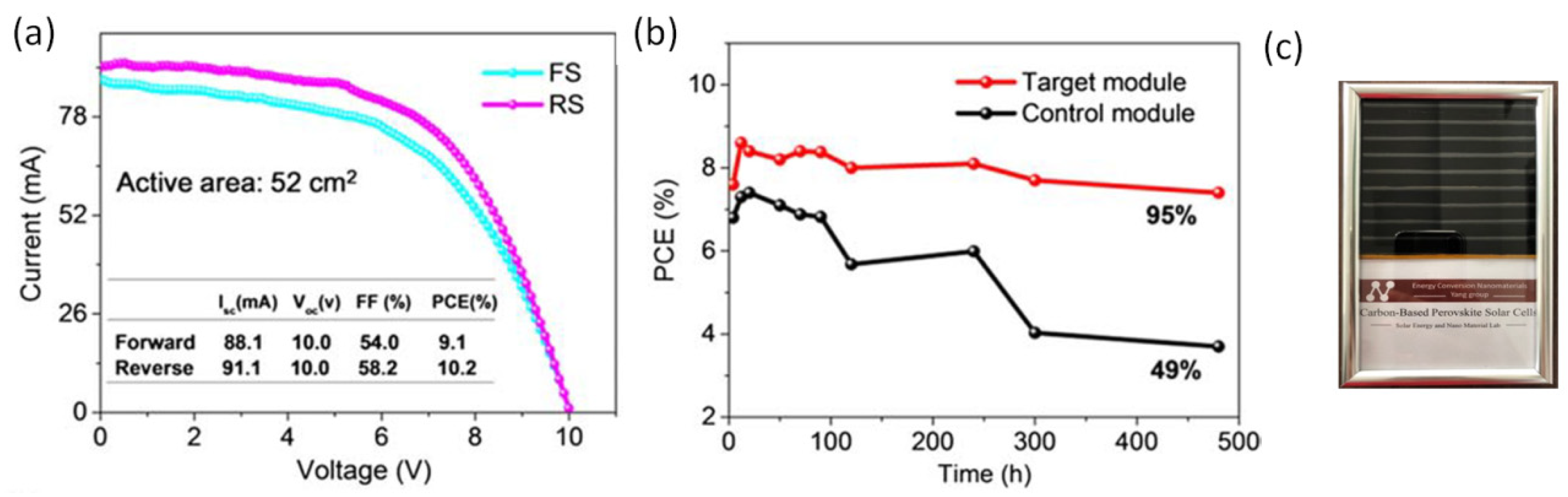
- Jin, J.; Yang, M.; Deng, W.; Xin, J.; Tai, Q.; Qian, J.; Dong, B.; Li, W.; Wang, J.; Li, J. Highly Efficient and Stable Carbon-Based Perovskite Solar Cells with the Polymer Hole Transport Layer. Sol. Ener. 2021, 220, 491–497. [Google Scholar] [CrossRef]
- Zhang, H.; Wang, H.; Williams, S.T.; Xiong, D.; Zhang, W.; Chueh, C.-C.; Chen, W.; Jen, A.K.-Y. SrCl2 Derived Perovskite Facilitating a High Efficiency of 16% in Hole-Conductor-Free Fully Printable Mesoscopic Perovskite Solar Cells. Adv. Mater. 2017, 29, 1606608. [Google Scholar] [CrossRef] [PubMed]
- Guan, Y.; Xu, M.; Zhang, W.; Li, D.; Hou, X.; Hong, L.; Wang, Q.; Zhang, Z.; Mei, A.; Chen, M.; et al. In Situ Transfer of CH3NH3PbI3 Single Crystals in Mesoporous Scaffolds for Efficient Perovskite Solar Cells. Chem. Sci. 2020, 11, 474–481. [Google Scholar] [CrossRef] [PubMed] [Green Version]
- Li, D.; Tong, C.; Ji, W.; Fu, Z.; Wan, Z.; Huang, Q.; Ming, Y.; Mei, A.; Hu, Y.; Rong, Y.; et al. Vanadium Oxide Post-Treatment for Enhanced Photovoltage of Printable Perovskite Solar Cells. ACS Sustain. Chem. Eng. 2019, 7, 2619–2625. [Google Scholar] [CrossRef]
- Tian, C.; Mei, A.; Zhang, S.; Tian, H.; Liu, S.; Qin, F.; Xiong, Y.; Rong, Y.; Hu, Y.; Zhou, Y.; et al. Oxygen Management in Carbon Electrode for High-Performance Printable Perovskite Solar Cells. Nano Energy 2018, 53, 160–167. [Google Scholar] [CrossRef]
- Chu, L.; Zhai, S.; Ahmad, W.; Zhang, J.; Zang, Y.; Yan, W.; Li, Y. High-Performance Large-Area Perovskite Photovoltaic Modules. Nano Res. Energy 2022, 1, e9120024. [Google Scholar] [CrossRef]
- Soto-Montero, T.; Soltanpoor, W.; Morales-Masis, M. Pressing Challenges of Halide Perovskite Thin Film Growth. APL Mater. 2020, 8, 110903. [Google Scholar] [CrossRef]
- Pradid, P.; Sanglee, K.; Thongprong, N.; Chuangchote, S. Carbon Electrodes in Perovskite Photovoltaics. Materials 2021, 14, 5989. [Google Scholar] [CrossRef]
- Suresh, R.R.; Lakshmanakumar, M.; Arockia Jayalatha, J.B.B.; Rajan, K.S.; Sethuraman, S.; Krishnan, U.M.; Rayappan, J.B.B. Fabrication of Screen-Printed Electrodes: Opportunities and Challenges. J. Mater. Sci. 2021, 56, 8951–9006. [Google Scholar] [CrossRef]
- Sarialtin, H.; Geyer, R.; Zafer, C. Life Cycle Assessment of Hole Transport Free Planar–Mesoscopic Perovskite Solar Cells. J. Renew. Sustain. Energy 2020, 12, 023502. [Google Scholar] [CrossRef]
- Okoroafor, T.; Maalouf, A.; Oez, S.; Babu, V.; Wilk, B.; Resalati, S. Life Cycle Assessment of Inkjet Printed Perovskite Solar Cells. J. Clean. Prod. 2022, 373, 133665. [Google Scholar] [CrossRef]
- Karavioti, A.; Chalkias, D.A.; Katsagounos, G.; Mourtzikou, A.; Kalarakis, A.N.; Stathatos, E. Toward a Scalable Fabrication of Perovskite Solar Cells under Fully Ambient Air Atmosphere: From Spin-Coating to Inkjet-Printing of Perovskite Absorbent Layer. Electronics 2021, 10, 1904. [Google Scholar] [CrossRef]
- Gao, L.; Chen, L.; Huang, S.; Li, X.; Yang, G. Series and Parallel Module Design for Large-Area Perovskite Solar Cells. ACS Appl. Energy Mater. 2019, 2, 3851–3859. [Google Scholar] [CrossRef]
- Walter, A.; Moon, S.J.; Kamino, B.A.; Löfgren, L.; Sacchetto, D.; Matteocci, F.; Taheri, B.; Bailat, J.; Di Carlo, A.; Ballif, C.; et al. Closing the Cell-to-Module Efficiency Gap: A Fully Laser Scribed Perovskite Minimodule With 16% Steady-State Aperture Area Efficiency. IEEE J. Photovolt. 2018, 8, 151–155. [Google Scholar] [CrossRef] [Green Version]
- Brooks, K.G.; Nazeeruddin, M.K. Laser Processing Methods for Perovskite Solar Cells and Modules. Adv. Energy Mater. 2021, 11, 2101149. [Google Scholar] [CrossRef]
- Palma, A.L. Laser-Processed Perovskite Solar Cells and Modules. Sol. RRL 2020, 4, 1900432. [Google Scholar] [CrossRef]
- Meroni, S.M.P.; Hooper, K.E.A.; Dunlop, T.; Baker, J.A.; Worsley, D.; Charbonneau, C.; Watson, T.M. Scribing Method for Carbon Perovskite Solar Modules. Energies 2020, 13, 1589. [Google Scholar] [CrossRef] [Green Version]
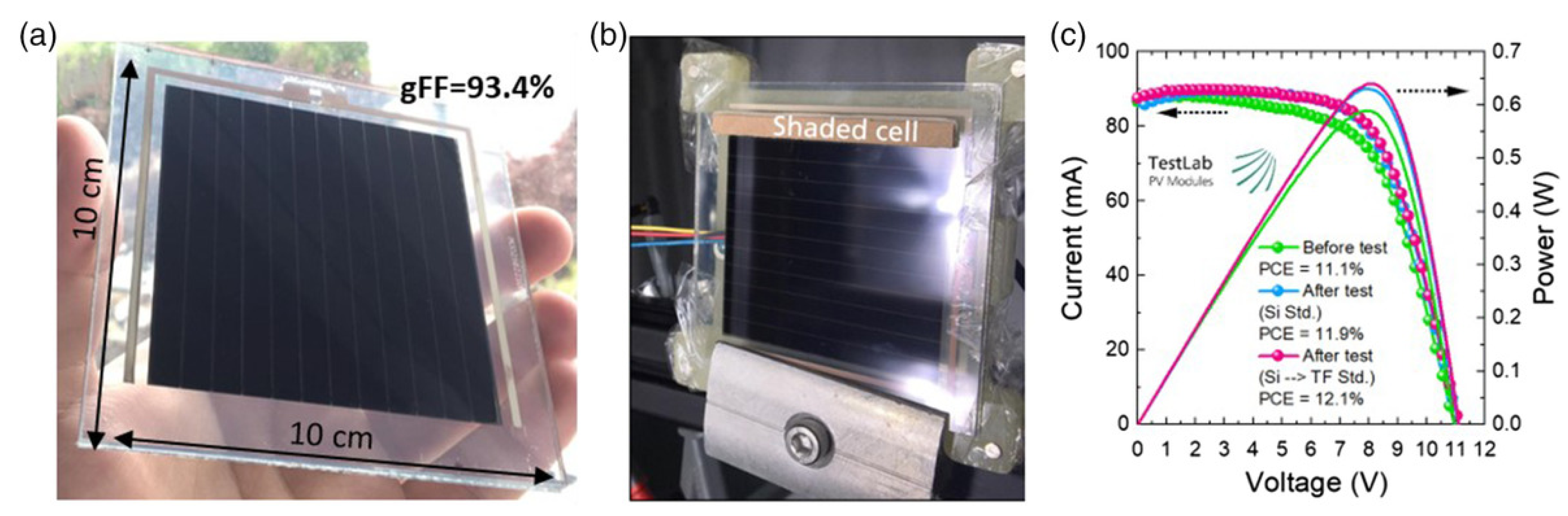
- Rakocevic, L.; Schöpe, G.; Turan, B.; Genoe, J.; Aernouts, T.; Haas, S.; Gehlhaar, R.; Poortmans, J. Perovskite Modules with 99% Geometrical Fill Factor Using Point Contact Interconnections Design. Prog. Photovolt. Res. Appl. 2020, 28, 1120–1127. [Google Scholar] [CrossRef]
- Priyadarshi, A.; Haur, L.J.; Murray, P.; Fu, D.; Kulkarni, S.; Xing, G.; Sum, T.C.; Mathews, N.; Mhaisalkar, S.G. A Large Area (70 cm2) Monolithic Perovskite Solar Module with a High Efficiency and Stability. Energy Environ. Sci. 2016, 9, 3687–3692. [Google Scholar] [CrossRef]
- Hashmi, S.G.; Martineau, D.; Li, X.; Ozkan, M.; Tiihonen, A.; Dar, M.I.; Sarikka, T.; Zakeeruddin, S.M.; Paltakari, J.; Lund, P.D.; et al. Air Processed Inkjet Infiltrated Carbon Based Printed Perovskite Solar Cells with High Stability and Reproducibility. Adv. Mater. Technol. 2017, 2, 1600183. [Google Scholar] [CrossRef]
- Grancini, G.; Roldán-Carmona, C.; Zimmermann, I.; Mosconi, E.; Lee, X.; Martineau, D.; Narbey, S.; Oswald, F.; De Angelis, F.; Grätzel, M.; et al. One-Year Stable Perovskite Solar Cells by 2D/3D Interface Engineering. Nat. Commun. 2017, 8, 15684. [Google Scholar] [CrossRef] [Green Version]
- Mei, A.; Li, X.; Liu, L.; Ku, Z.; Liu, T.; Rong, Y.; Xu, M.; Hu, M.; Chen, J.; Yang, Y.; et al. A Hole-Conductor-Free, Fully Printable Mesoscopic Perovskite Solar Cell with High Stability. Science 2014, 345, 295–298. [Google Scholar] [CrossRef] [PubMed]
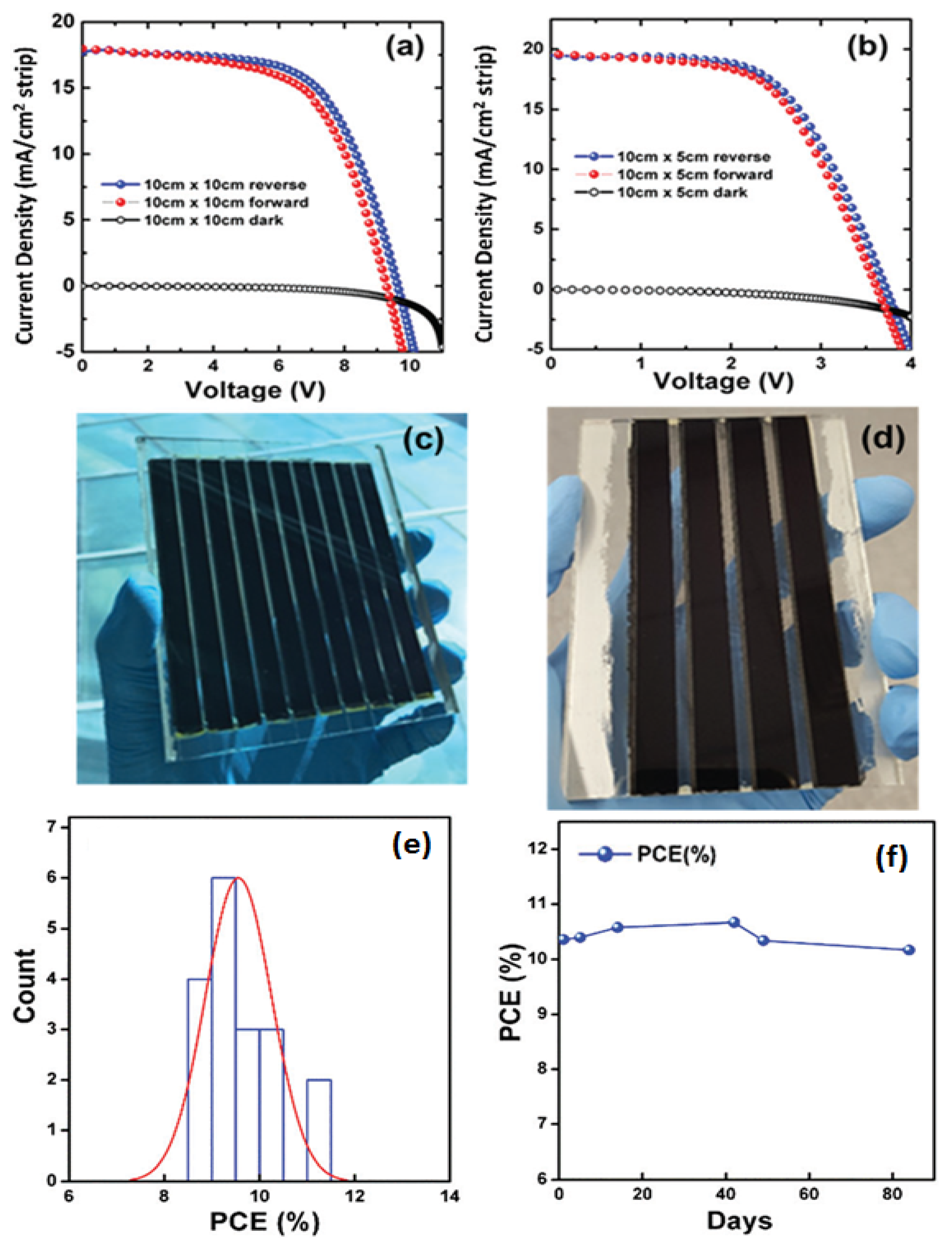
- Hu, Y.; Si, S.; Mei, A.; Rong, Y.; Liu, H.; Li, X.; Han, H. Stable Large-Area (10 × 10 cm2) Printable Mesoscopic Perovskite Module Exceeding 10% Efficiency. Sol. RRL 2017, 1, 1600019. [Google Scholar] [CrossRef]
- Chalkias, D.A.; Mourtzikou, A.; Katsagounos, G.; Karavioti, A.; Kalarakis, A.N.; Stathatos, E. Suppression of Coffee-Ring Effect in Air-Processed Inkjet-Printed Perovskite Layer toward the Fabrication of Efficient Large-Sized All-Printed Photovoltaics: A Perovskite Precursor Ink Concentration Regulation Strategy. Sol. RRL 2022, 6, 2200196. [Google Scholar] [CrossRef]
- Bashir, A.; Shukla, S.; Lew, J.H.; Shukla, S.; Bruno, A.; Gupta, D.; Baikie, T.; Patidar, R.; Akhter, Z.; Priyadarshi, A.; et al. Spinel Co3O4 Nanomaterials for Efficient and Stable Large Area Carbon-Based Printed Perovskite Solar Cells. Nanoscale 2018, 10, 2341–2350. [Google Scholar] [CrossRef] [PubMed]
- Bashir, A.; Lew, J.H.; Shukla, S.; Gupta, D.; Baikie, T.; Chakraborty, S.; Patidar, R.; Bruno, A.; Mhaisalkar, S.; Akhter, Z. Cu-Doped Nickel Oxide Interface Layer with Nanoscale Thickness for Efficient and Highly Stable Printable Carbon-Based Perovskite Solar Cell. Sol. Ener. 2019, 182, 225–236. [Google Scholar] [CrossRef]
- Raptis, D.; Stoichkov, V.; Meroni, S.M.P.; Pockett, A.; Worsley, C.A.; Carnie, M.; Worsley, D.A.; Watson, T. Enhancing Fully Printable Mesoscopic Perovskite Solar Cell Performance Using Integrated Metallic Grids to Improve Carbon Electrode Conductivity. Curr. Appl. Phys. 2020, 20, 619–627. [Google Scholar] [CrossRef]
- Xu, M.; Ji, W.; Sheng, Y.; Wu, Y.; Cheng, H.; Meng, J.; Yan, Z.; Xu, J.; Mei, A.; Hu, Y.; et al. Efficient Triple-Mesoscopic Perovskite Solar Mini-Modules Fabricated with Slot-Die Coating. Nano Energy 2020, 74, 104842. [Google Scholar] [CrossRef]
- Cai, L.; Liang, L.; Wu, J.; Ding, B.; Gao, L.; Fan, B. Large Area Perovskite Solar Cell Module. J. Semicond. 2017, 38, 014006. [Google Scholar] [CrossRef]
- De Rossi, F.; Baker, J.A.; Beynon, D.; Hooper, K.E.A.; Meroni, S.M.P.; Williams, D.; Wei, Z.; Yasin, A.; Charbonneau, C.; Jewell, E.H.; et al. All Printable Perovskite Solar Modules with 198 cm2 Active Area and Over 6% Efficiency. Adv. Mater. Technol. 2018, 3, 1800156. [Google Scholar] [CrossRef] [Green Version]
- Worsley, C.; Raptis, D.; Meroni, S.M.P.; Patidar, R.; Pockett, A.; Dunlop, T.; Potts, S.J.; Bolton, R.; Charbonneau, C.M.E.; Carnie, M.; et al. Green Solvent Engineering for Enhanced Performance and Reproducibility in Printed Carbon-Based Mesoscopic Perovskite Solar Cells and Modules. Mater. Adv. 2022, 3, 1125–1138. [Google Scholar] [CrossRef]
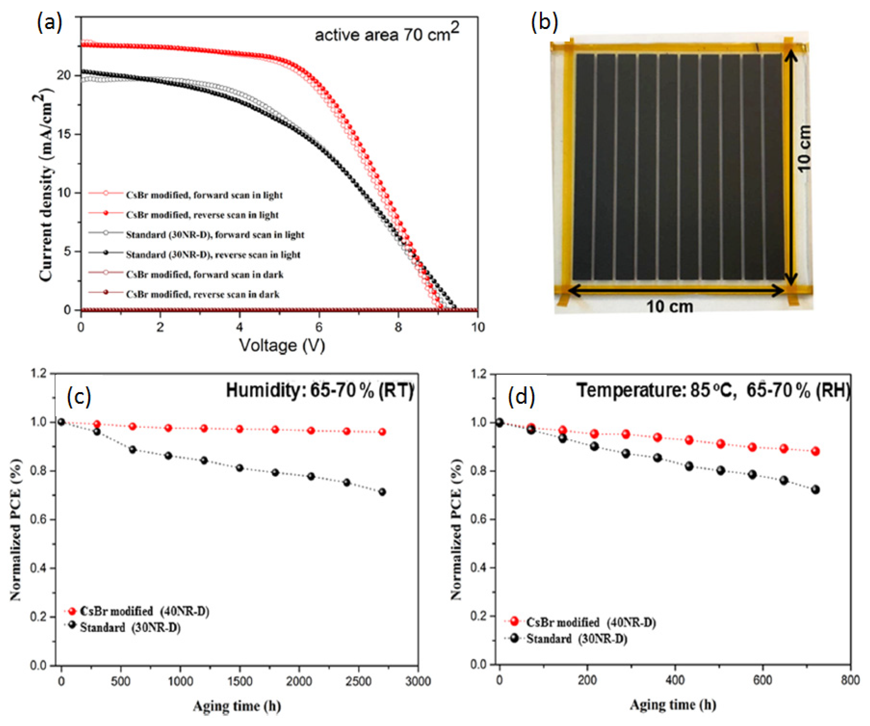
- Keremane, K.S.; Prathapani, S.; Haur, L.J.; Bruno, A.; Priyadarshi, A.; Adhikari, A.V.; Mhaisalkar, S.G. Improving the Performance of Carbon-Based Perovskite Solar Modules (70 cm2) by Incorporating Cesium Halide in Mesoporous TiO 2. ACS Appl. Energy Mater. 2021, 4, 249–258. [Google Scholar] [CrossRef]
- Bogachuk, D.; Saddedine, K.; Martineau, D.; Narbey, S.; Verma, A.; Gebhardt, P.; Herterich, J.P.; Glissmann, N.; Zouhair, S.; Markert, J.; et al. Perovskite Photovoltaic Devices with Carbon-Based Electrodes Withstanding Reverse-Bias Voltages up to –9 V and Surpassing IEC 61215:2016 International Standard. Sol. RRL 2022, 6, 2100527. [Google Scholar] [CrossRef]
- Lou, L.; Liu, T.; Xiao, J.; Xiao, S.; Long, X.; Zheng, S.; Yang, S. Controlling Apparent Coordinated Solvent Number in the Perovskite Intermediate Phase Film for Developing Large-Area Perovskite Solar Modules. Energy Technol. 2020, 8, 1900972. [Google Scholar] [CrossRef]
- Ghosh, S.; Mishra, S.; Singh, T. Antisolvents in Perovskite Solar Cells: Importance, Issues, and Alternatives. Adv. Mater. Interfaces 2020, 7, 2000950. [Google Scholar] [CrossRef]
- He, S.; Qiu, L.; Son, D.-Y.; Liu, Z.; Juarez-Perez, E.J.; Ono, L.K.; Stecker, C.; Qi, Y. Carbon-Based Electrode Engineering Boosts the Efficiency of All Low-Temperature-Processed Perovskite Solar Cells. ACS Energy Lett. 2019, 4, 2032–2039. [Google Scholar] [CrossRef]
- Chen, H.; Wei, Z.; He, H.; Zheng, X.; Wong, K.S.; Yang, S. Solvent Engineering Boosts the Efficiency of Paintable Carbon-Based Perovskite Solar Cells to Beyond 14%. Adv. Energy Mater. 2016, 6, 1502087. [Google Scholar] [CrossRef]
- Sun, Q.; Shen, C.; Wang, D.; Zhang, T.; Ban, H.; Shen, Y.; Zhang, Z.; Zhang, X.-L.; Yang, G.; Wang, M. Efficient and Stable Large-Area Perovskite Solar Cells with Inorganic Perovskite/Carbon Quantum Dot-Graded Heterojunction. Research 2021, 2021, 1–10. [Google Scholar] [CrossRef]
- Han, J.; Yin, X.; Zhou, Y.; Nan, H.; Gu, Y.; Tai, M.; Li, J.; Lin, H. High Efficient Large-Area Perovskite Solar Cells Based on Paintable Carbon Electrode with NiO Nanocrystal-Carbon Intermediate Layer. Chem. Lett. 2019, 48, 734–737. [Google Scholar] [CrossRef] [Green Version]
- Babu, V.; Fuentes Pineda, R.; Ahmad, T.; Alvarez, A.O.; Castriotta, L.A.; Di Carlo, A.; Fabregat-Santiago, F.; Wojciechowski, K. Improved Stability of Inverted and Flexible Perovskite Solar Cells with Carbon Electrode. ACS Appl. Energy Mater. 2020, 3, 5126–5134. [Google Scholar] [CrossRef]
- Liu, H.; Geng, C.; Wei, P.; Chen, H.; Zheng, S.; Wang, H.; Xie, Y. Improving the Performance and Stability of Large-Area Carbon-Based Perovskite Solar Cells Using N, O Co-Doped Biomass Porous Carbon. J. Alloy. Compd. 2022, 912, 165123. [Google Scholar] [CrossRef]
- Verma, A.; Martineau, D.; Abdolhosseinzadeh, S.; Heier, J.; Nüesch, F. Inkjet Printed Mesoscopic Perovskite Solar Cells with Custom Design Capability. Mater. Adv. 2020, 1, 153–160. [Google Scholar] [CrossRef]
- Mali, S.S.; Kim, H.; Kim, H.H.; Park, G.R.; Shim, S.E.; Hong, C.K. Large Area, Waterproof, Air Stable and Cost Effective Efficient Perovskite Solar Cells through Modified Carbon Hole Extraction Layer. Mater. Today Chem. 2017, 4, 53–63. [Google Scholar] [CrossRef]
- Li, D.; Jiang, P.; Zhang, W.; Du, J.; Qiu, C.; Liu, J.; Hu, Y.; Rong, Y.; Mei, A.; Han, H. Series Resistance Modulation for Large-Area Fully Printable Mesoscopic Perovskite Solar Cells. Sol. RRL 2022, 6, 2100554. [Google Scholar] [CrossRef]
- Mariani, P.; Najafi, L.; Bianca, G.; Zappia, M.I.; Gabatel, L.; Agresti, A.; Pescetelli, S.; Di Carlo, A.; Bellani, S.; Bonaccorso, F. Low-Temperature Graphene-Based Paste for Large-Area Carbon Perovskite Solar Cells. ACS Appl. Mater. Interfaces 2021, 13, 22368–22380. [Google Scholar] [CrossRef] [PubMed]
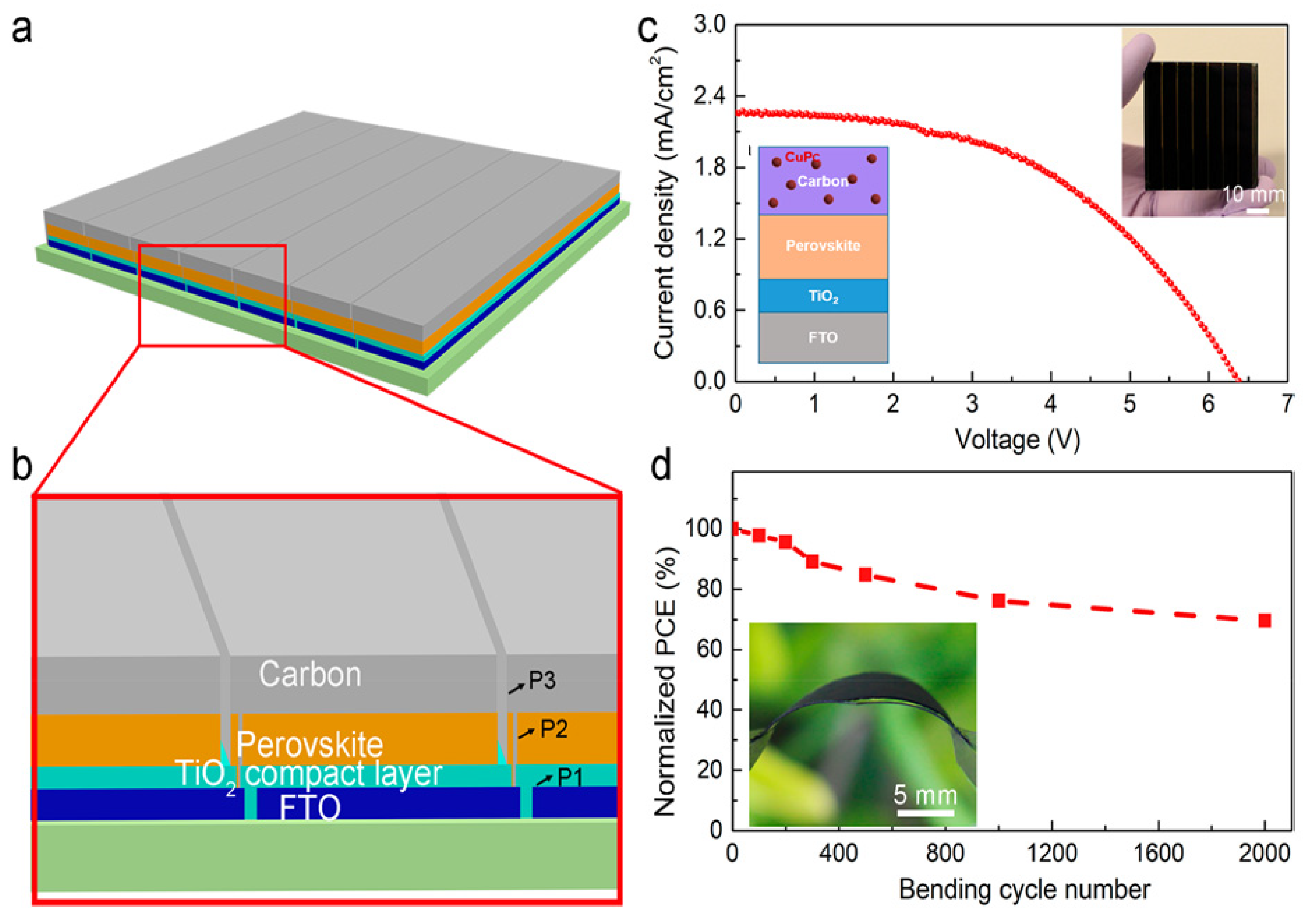
- Han, J.; Yin, X.; Zhou, Y.; Nan, H.; Gu, Y.; Tai, M.; Li, J.; Lin, H. Perovskite/Poly[Bis(4-Phenyl)(2,4,6-Trimethylphenyl)Amine] Bulk Heterojunction for High-Efficient Carbon-Based Large-Area Solar Cells by Gradient Engineering. ACS Appl. Mater. Interfaces 2018, 10, 42328–42334. [Google Scholar] [CrossRef]
- Peng, C.; Su, H.; Li, J.; Duan, Q.; Li, Q.; Xiao, J.; Ku, Z.; Zhong, J.; Li, W.; Peng, Y.; et al. Scalable, Efficient and Flexible Perovskite Solar Cells with Carbon Film Based Electrode. Sol. Energy Mater. Sol. Cells 2021, 230, 111226. [Google Scholar] [CrossRef]
- Cai, M.; Wu, Y.; Chen, H.; Yang, X.; Qiang, Y.; Han, L. Cost-Performance Analysis of Perovskite Solar Modules. Adv. Sci. 2017, 4, 1600269. [Google Scholar] [CrossRef]
- Song, Z.; McElvany, C.L.; Phillips, A.B.; Celik, I.; Krantz, P.W.; Watthage, S.C.; Liyanage, G.K.; Apul, D.; Heben, M.J. A Technoeconomic Analysis of Perovskite Solar Module Manufacturing with Low-Cost Materials and Techniques. Energy Environ. Sci. 2017, 10, 1297–1305. [Google Scholar] [CrossRef]
- Kajal, P.; Verma, B.; Vadaga, S.G.R.; Powar, S. Costing Analysis of Scalable Carbon-Based Perovskite Modules Using Bottom Up Technique. Glob. Chall. 2022, 6, 2100070. [Google Scholar] [CrossRef]


| CE Material | Type of QD | Electrolyte | PCE | Year | Ref. |
|---|---|---|---|---|---|
| MC/Ti | CdSe0.65Te0.35 | polysulfide | 11.16 | 2016 | [31] |
| MC/Ti | Zn–Cu–In–Se | polysulfide | 11.61 | 2016 | [32] |
| N-doped MC/Ti | Zn–Cu–In–Se | polysulfide | 12.07 | 2017 | [33] |
| MC/Ti | Zn–Cu–In–Se | polysulfide | 12.57 | 2017 | [34] |
| MC/Ti | Zn-Cu-In-Se/CdSe | polysulfide + PVP | 12.75 | 2018 | [35] |
| MC/Ti | Cu–In0.7–Ga0.3–Se | polysulfide | 11.49 | 2017 | [36] |
| Active Area (cm2) | Fabrication Method | Structure (with Respect to C Electrode) | Perovskite | PCE (%) | Comments | Ref. |
|---|---|---|---|---|---|---|
| 1 | Spin coating—C paste printing | LT mesoporous | CH3NH3PbI3 | 9.72 | IPA/CYHEX solvent in perovskite precursor solution | [110] |
| 1 | Spin coating—C paste doctor blading | LT mesoporous | CsPbI2.5Br0.5 | 13.35 | F-doped carbon quantum dots in the perovskite layer | [111] |
| 1 | Spin coating—C paste doctor blading | LT mesoporous | CH3NH3PbI3-xBrx | 12.5 | NiO-C intermediate layer | [112] |
| 1 | Spin coating—C paste blade coating | LT planar | Cs0.04(MA0.17FA0.83)0.96Pb(I0.83Br0.17)3 | 15.18 | Inverted structure/flexible device/Cr buffer layer | [113] |
| 1 | Spin coating—C paste doctor blading | LT mesoporous | CH3NH3PbI3 | 11.08 | N, O co-doped biomass porous composite carbon electrode based on activated soybean dregs carbon (SDC) | [114] |
| 1.5 | Inkjet printing—C screen printed | HT triple mesoscopic | CH3NH3PbI3 | 9.1 | Fully printed | [115] |
| 1 | Spin coating—C paste doctor blading | LT mesoporous | CH3NH3PbI3-xClx | 13.04 | C + CH3NH3I as HTM | [116] |
| 1 | Screen printing | HT triple mesoscopic | (5-AVAI) CH3NH3PbI3 | 13.99 | additional hot-pressed highly conductive LT carbon layer on the back carbon electrode | [117] |
| 3.49 | Spin coating—C paste doctor blading | LT mesoporous | Cs0.05(FA0.85MA0.15)0.95Pb(I0.85Br0.15)3 | 13.86 | Spiro-OMeTAD HTM/graphene-doped TiO2 | [118] |
| 1 | Spin coating—C paste doctor blading | LT mesoporous | CH3NH3PbI3 | 13 | PTAA HTM in the antisolvent | [119] |
| 1 | Spin coating—press transfer | Planar n-i-p | Cs0.05(FA0.85MA0.15)0.95Pb(I0.85Br0.15)3 | 14.05 | C cloth film electrode/spiro-OMeTAD HTM/flexible device | [120] |
| 1 | Spin coating—press transfer | Planar n-i-p | Cs0.05(FA0.85MA0.15)0.95Pb(I0.85Br0.15)3 | 17.02 | carbon film electrode composited with graphite paper/spiro-OMeTAD HTM | [60] |
Disclaimer/Publisher’s Note: The statements, opinions and data contained in all publications are solely those of the individual author(s) and contributor(s) and not of MDPI and/or the editor(s). MDPI and/or the editor(s) disclaim responsibility for any injury to people or property resulting from any ideas, methods, instructions or products referred to in the content. |
© 2023 by the authors. Licensee MDPI, Basel, Switzerland. This article is an open access article distributed under the terms and conditions of the Creative Commons Attribution (CC BY) license (https://creativecommons.org/licenses/by/4.0/).
Share and Cite
Bidikoudi, M.; Stathatos, E. Carbon Electrodes: The Rising Star for PSC Commercialization. Electronics 2023, 12, 992. https://doi.org/10.3390/electronics12040992
Bidikoudi M, Stathatos E. Carbon Electrodes: The Rising Star for PSC Commercialization. Electronics. 2023; 12(4):992. https://doi.org/10.3390/electronics12040992
Chicago/Turabian StyleBidikoudi, Maria, and Elias Stathatos. 2023. "Carbon Electrodes: The Rising Star for PSC Commercialization" Electronics 12, no. 4: 992. https://doi.org/10.3390/electronics12040992