Article

A Reconfigurable Setup for the On-Wafer Characterization of the Dynamic RON of 600 V GaN Switches at Variable Operating Regimes

by
Alessio Alemanno
,
Alberto Maria Angelotti
,
Gian Piero Gibiino
,
Alberto Santarelli
,
Enrico Sangiorgi
and
Corrado Florian
*
Department of Electrical, Electronic, and Information Engineering “Guglielmo Marconi”, University of Bologna, 40136 Bologna, Italy
*
Author to whom correspondence should be addressed.
Electronics 2023, 12(4), 1063; https://doi.org/10.3390/electronics12041063
Submission received: 19 January 2023 / Revised: 13 February 2023 / Accepted: 16 February 2023 / Published: 20 February 2023

Abstract

:
Charge-trapping mechanisms observed in high-voltage GaN switches are responsible for the degradation of power converter efficiency due to modulation of the effective dynamic ON-resistance ( R O N ) with respect to its static value. Dynamic R O N degradation is typically dependent on the blocking voltage and the commutation frequency and is particularly significant in new technologies under development. The possibility to characterize this phenomenon on GaN switch samples directly on-wafer, under controlled operating conditions that resemble real operations of the DUT in a switching mode power converter is extremely valuable in the development phase of new technologies or for quality verification of production wafers. In this paper, we describe a setup that allows this characterization: dynamic R O N degradation of on-wafer 600 V GaN switches is characterized as a function of the V D S blocking voltage, the V G S driving voltage, and at different temperatures. The dependency on the switching frequency is identified by measuring the current recovery of the switch after the application of blocking voltages of different durations.

1. Introduction

Wide band gap (WBG) semiconductors have recently become an important reality in the power electronic converter market and their intrinsic superior performance with respect to Si-based counterparts [1,2,3] is progressively increasing the number of applications where they become the preferred choice since their added value justifies the nominally larger cost per part. Probably the most important field of application of power WBG technology is the automotive industry, which is under a tremendous renovation towards vehicle electrification [4,5]. As a matter of fact, the main power converters of an electric or hybrid vehicle, namely the traction inverter, the DC-DC high voltage bus converter, and the on-board battery charger, are components that gain exceptional advantages from the exploitation of WBG devices since the higher volumetric power density and higher efficiency achieved by exploiting these technologies enable components miniaturization, extend the vehicle range, and shorten the charging time. In particular, low conduction resistance R O N and low gate charge and parasitic capacitances are the key parameters of WBG devices that provide low conduction and switches losses, enabling higher switching frequency operation with associated high efficiency [6].
Between WBG technologies, silicon carbide (SiC) power switches have already achieved popularity: these switches are commercially available from a fairly large number of providers [7] and several end-user products exploiting this technology are present in the market [8].
GaN power switch technologies have shown the potential to further increase power converter performances due to their even better R D S × Q G figure of merit (FOM). GaN transistors are HEMT devices (high electron mobility transistors) based on a complex AlGaN/GaN hetero-epitaxy structure that provides very high charge density and mobility. They are lateral conduction devices derived from RF/microwave GaN transistor technologies that apply, among others, techniques to further increase the breakdown voltage [9] and to shift the gate voltage threshold to a positive value, thus obtaining enhance-mode normally off power switches [10], which are the sole product employable in some power applications (for RF/microwave applications, GaN HEMTs are normally on devices). As a matter of fact, the technological process for obtaining normally off devices, while maintaining high conduction and dynamic characteristics, has historically required several process iterations. Thus, at present GaN technology is less mature than SiC and only a few providers can offer high voltage (i.e., >600 V) commercial GaN switches with the performance and reliability levels required by automotive applications [11,12,13,14]. Nonetheless, given the enormous potential of this technology, all the main providers of power electronic devices are pursuing the optimization of their power GaN devices and then several foundries are working towards the development and optimization of these processes.
One well-known and peculiar issue of GaN transistors is the presence of charge-trapping effects, which are responsible for the modulation of the charges available for current conduction, with a consequent degradation of the conductivity of the channel during dynamic regimes. This issue has been largely investigated in more mature RF/microwave technologies where trap-related phenomena are responsible for power amplifiers’ efficiency degradation and signal distortion [15,16,17,18]. In power device technologies, these phenomena have a direct effect on the increment of the ON-resistance in dynamic regime with respect to its static (DC) value.
This dynamic R O N degradation proportionally increases the converter conduction losses. In the literature, a large interest can be found for both the identification of the physical mechanisms that support these phenomena [19] and their characterization [20,21]. A good understanding of physics-based modeling is helpful for the optimization of the technologies, whereas a precise characterization is fundamental for performance assessment. The physical description of these phenomena is beyond the scope of this paper; nonetheless, it is interesting to observe that R O N degradation is a function of the application voltages, of the switching frequency and varies with temperature [10,21]. Indeed, it has been observed that the trapping state density increases with the electric field and then with the blocking voltage applied at the device terminal during the OFF state in dynamic switching-mode operation. For the same reasons, the gate driving voltage can also play a role in this mechanism. As for dynamic effects, the charge-trapping and release-time constants (that give the frequency dependency of dynamic R O N modulation) vary with the technological solutions and their energy levels are a function of the temperature.
In this context, this paper describes a measurement set-up for a precise characterization of the dynamic R O N of high-voltage on-wafer devices with the possibility to modify the V D S blocking voltage, the V G S gate driving voltage, the commutation period, and the temperature to assess the impact of each contribution. This type of setup can be valuable for foundries to test different solutions of experimental devices during the optimization of a new process and for the quality verification of production wafers. Indeed, since it is associated with trapping phenomena, the wafer to wafer dispersion of the dynamic R O N can be also considered an indication of possible reliability concerns. The proposed measurement methodology is described in Section 2; Section 3 describes the implemented setup; the experimental measurements are provided in Section 4.

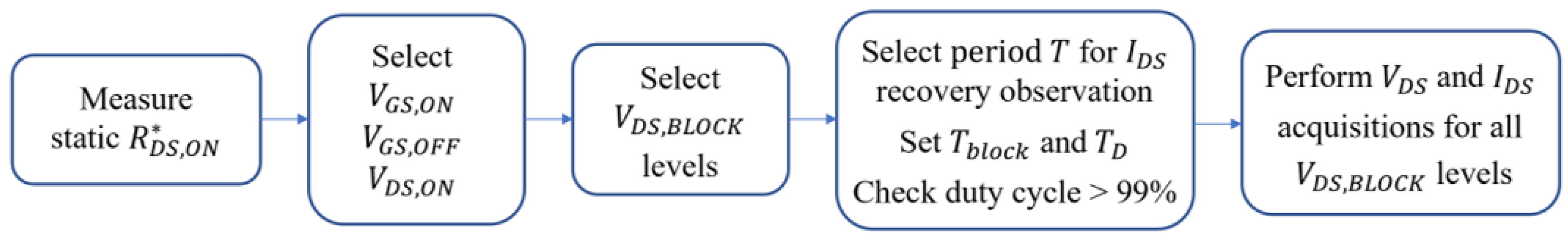
2. Dynamic Measurement Methodology

The proposed time-domain technique for the evaluation of the power switch DUT R D S , O N is described in this section. The DUT is measured under a periodic isothermal regime described in the waveforms of Figure 1. The diagram of Figure 2 summarizes the measurement procedure settings and steps. During the period, the DUT is switched between a bias state ( V G S , O N , V D S , O N ) and a blocking state ( V G S , O F F , V D S , B l o c k ) . As described in the waveforms of Figure 1, a short safety margin T D (500 ns, as will be described in the next section) between V G S and V D S transitions is used to avoid over-currents at the application/release of the blocking voltage V D S , B l o c k . The blocking state duration is negligible with respect to the period, thus the DUT is biased in the selected bias state for more than 99% of the period (i.e., the V G S waveform duty cycle is more than 99%). The bias state ( V G S , O N , V D S , O N ) is selected so that the corresponding I D S , O N meets the following requirements: (1) it must be large enough to enable high-accuracy current sensing; (2) it must be small enough to induce a negligible power dissipation ( P D I S S = R D S , O N · I D S , O N 2 ) so that the DUT can be considered isothermal with the thermal chuck of the probe station over which is placed during the entire duration of the measurement.
In this way, thermal effects are not involved in the observed dynamics of the drain current, and they can be exclusively ascribed to trapping/de-trapping mechanisms. During the application of the blocking voltage in T B l o c k , the combination ( V G S , O F F , V D S , B l o c k ) applies high electric fields to the DUT channel that trigger charge trapping phenomena, as in switching-mode power converter operation. By reapplying the same bias state ( V G S , O N , V D S , O N ) after the blocking event, the slow recovery of the drain current towards the I D S , O N can be observed. If the period duration is selected large enough to complete the entire de-trapping mechanism, I D S , O N at the end of the period can be considered the static value of the current, and the corresponding value of the ratio R D S , O N ( T P ) = R D S , O N * = V D S ( T P ) / I D S ( T P ) at the end of the period T P the static R D S , O N * . The result of this characterization is the dynamic variation of R D S , O N over time after the blocking voltage event that triggers the trap capture, which is the lower plot in Figure 1. This gives an immediate indication of the time constants related to the de-trapping mechanisms, which is a useful input for process evaluation and physical modeling. On the other hand, a direct indication related to the application can also be obtained considering the inverse of the recovery time f s = 1 / T r e c o v e r y as the corresponding switching frequency of the application: in this way, R D S , O N degradation for the actual switching frequency of the application can be evaluated. By varying the values of V D S , B l o c k and V G S , O F F , the dependence of R D S , O N degradation from applied voltages is assessed. Finally, by varying the thermal chuck temperature (and thus the DUT temperature since it is practically iso-thermal) the effect of temperature can also be evaluated; indeed, trap energy states are temperature dependent. The proposed setup can implement this characterization with the flexibility to vary all the described parameters. The main challenges of this implementation are the capability to apply precise dynamic high voltage excitations to the DUT and to realize precise and noiseless dynamic sensing of current/voltages for the computation of the dynamic R D S , O N .

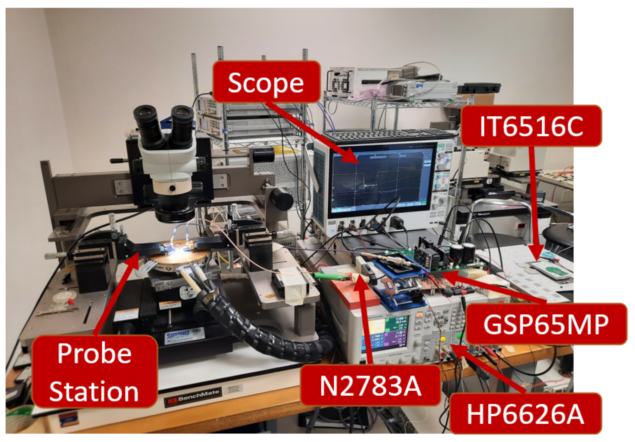
3. Setup Description

A functional simplified description of the setup is illustrated in Figure 3. The DUT is placed in a probe station where gate, source, and drain pads are directly contacted with low-parasitic on-wafer probes, while a thermally controlled chuck (Temptronic TP03215A) sets the working temperature beneath the wafer or the metal carrier used for soldering bare die device samples.
The V D S excitation switching between ( V D S , O N , V D S , B l o c k ) values needs to be provided by an isolated and fast switching leg that alternatively connects the DUT drain pad between two isolated voltage sources at V D S , O N and V D S , B l o c k values provided by dedicated power supplies. The DUT I D S , O N and V D S , O N are sensed by current/voltage probes and acquired by a digital oscilloscope. A more detailed description of the implemented set-up is provided in Figure 4.
The probe station is a Cascade Microtech Summit 9000 equipped with a Temptronic ThermoChuck system. In order to reproduce excitations similar to operative regimes, the switching leg needs to have dynamic characteristics similar to the DUT. Thus, it is realized by exploiting the GSP65MB Evaluation Board of the GaN system [22]: this is basically a half-bridge exploiting commercial 25 mΩ, 650 V GaN HEMT devices (which represent the state-of-the-art high-voltage GaN switches), Silicon Labs Si4121 isolated gate drivers, dead-time logic circuitry for selectable dead-time control, and local low-inductance DC-link capacitors to sustain fast commutations without voltage drops. The DC supplies for the bias V D S , O N and blocking voltage V D S , B l o c k generation are Agilent N6705B and ITECH IT6516C, respectively. The Agilent 81150A arbitrary waveform generator is used to control the switching leg (PWM2 in the figure) and to directly control the DUT gate (PWM1 in the figure), assuring the required synchronization to the two excitations ( V G S , V D S ) . Wide-band current sensing is provided with Keysight 100 MHz N2783A current probe with 1% accuracy. The sensing of the device V D S is quite complex because of the required dynamic range: the characterization procedure needs to measure high V D S , B l o c k i n g during the device switch-OFF to verify the blocking voltage and its synchronization with the DUT V G S , and very low V D S , O N during device conduction for an accurate evaluation of R D S , O N . In particular, for 600 V GaN switch technology, the maximum V D S , B l o c k is in the order of 400 V and V D S , O N in the order of mV. For this reason, a single acquisition channel for V D S is not a viable solution, but two different methods are used simultaneously, as described in Figure 4. A first acquisition channel uses the isolated active differential probe with 40 MHz bandwidth Aaronia ADP1 to acquire the entire evolution of V D S in the period and scale it 100:1 to fit the oscilloscope voltage range: this is useful to monitor V D S , B l o c k and the synchronization with V G S , but this acquisition does not have enough sensitivity for a precise and useful acquisition of V D S , O N . For this acquisition, a high sensitivity and wide-band acquisition channel is implemented in a dedicated PCB exploiting the low-offset and low-noise Analog Devices AD797 operational amplifier in the ×20 voltage gain configuration described in the inset of Figure 4. This acquisition channel enables the accurate characterization of a V D S waveform below 1 mV. As described in [23], with this configuration, the Op-Amp input is protected by means of two TVS diodes in antiparallel configuration from high-voltage V D S , B l o c k . This solution avoids the saturation of the oscilloscope acquisition channel and largely limits the saturation of the Op-Amp. As a consequence, a few μs after the blocking event, the Op-Amp exits saturation and is capable of correctly measuring V D S , O N , and then R D S , O N can be computed. Finally, a simple passive probe is used to sense the driving voltage V G S applied to the DUT. The digital oscilloscope used in the setup is Tektronix MSO-56 scope. A picture of the entire setup is provided in Figure 5.

4. Experimental Characterization of 600 V GaN Switches

The described measurement setup is used to characterize the dynamic ON-resistance of 600 V GaN transistors. The transistors are p-GaN e-mode HEMTs on a silicon substrate coming from an experimental wafer of a process in the development phase in a research foundry. The preliminary electrical specifications of the switches are shown in Table 1. The very low values of parasitics are indicative of the capability of this technology for high-switching frequencies.
The transistor dies have been soldered to a metal carrier and contacted with on-wafer micro-probes as described in the pictures of Figure 6.

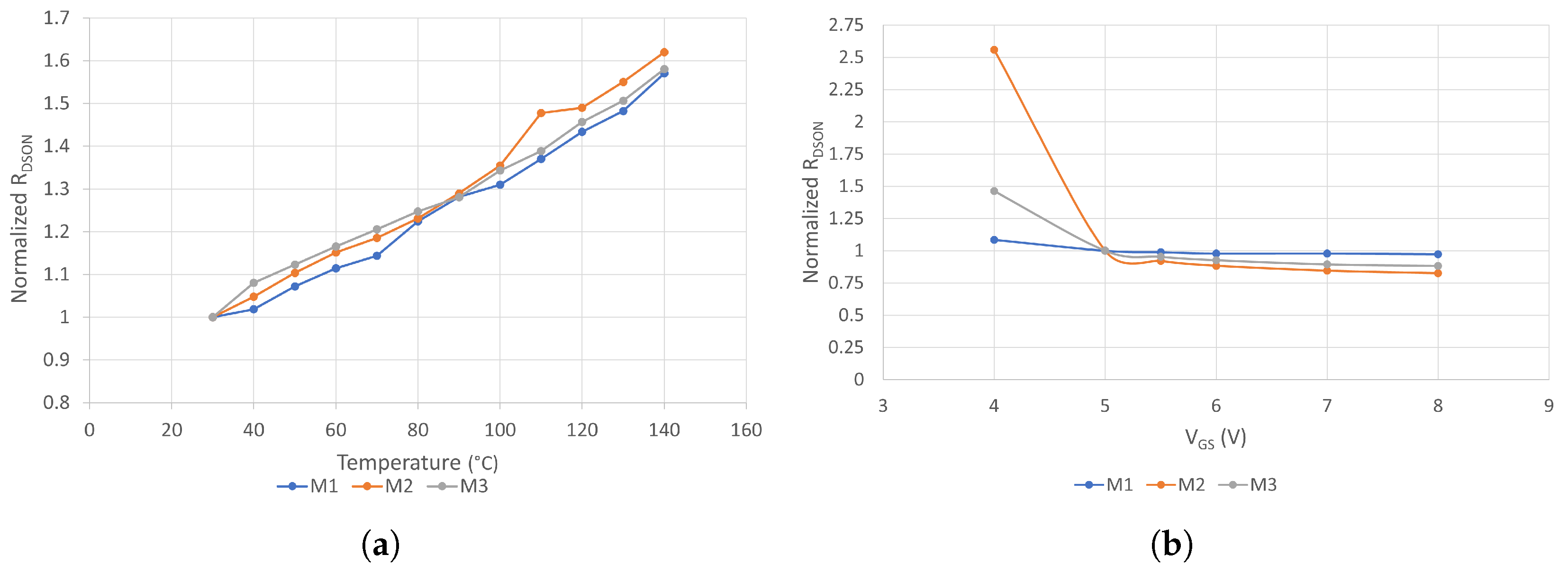
4.1. Static Measurements

For the evaluation of the dynamic ON-resistance degradation, the static R D S , O N must be identified. A de-embedding procedure based on the measurement of the parasitic resistance of the setup when the DUT is replaced by a short circuit was performed. As discussed before, to guarantee iso-thermal conditions in temperature-dependent measurements of the sole trapping phenomena, the DUT must be properly biased to show negligible self-heating compared to the temperature controlled by the chuck. Thus a “measuring” bias current of 500 mA was selected as a good compromise between current measurement accuracy and device self-heating. Indeed, since the estimated thermal resistance of the DUT is 2.2 °C/W and the static R D S , O N around 0.5 Ω, the dissipated power is about 125 mW with a resulting negligible temperature increase Δ T = 0.275 °C. This bias current was used for both static and dynamic measurements, which can consequently be considered isothermal. The static R D S , O N of three samples (M1, M2, and M3) was measured at increasing temperatures up to 140 °C (maximum rating of the probes); the results are shown in Figure 7a, where the R D S , O N is normalized to the reference value at 30 °C. Additional static measurements were carried out at different V G S to evaluate the gate driving voltage requirements. The results are shown in Figure 7b, where the static R D S is plotted versus the gate driving voltage and normalized to the value at V G S = 5 V. Above V G S = 5 V, all the samples are fully ON since the channel resistance reveals a negligible improvement for higher voltages, whilst for V G S = 4 V the devices show different behaviors probably due to a shift of threshold voltage which is expected for a young technological process [24]. Hence, V G S , O N = 5 V is chosen for dynamic measurements.

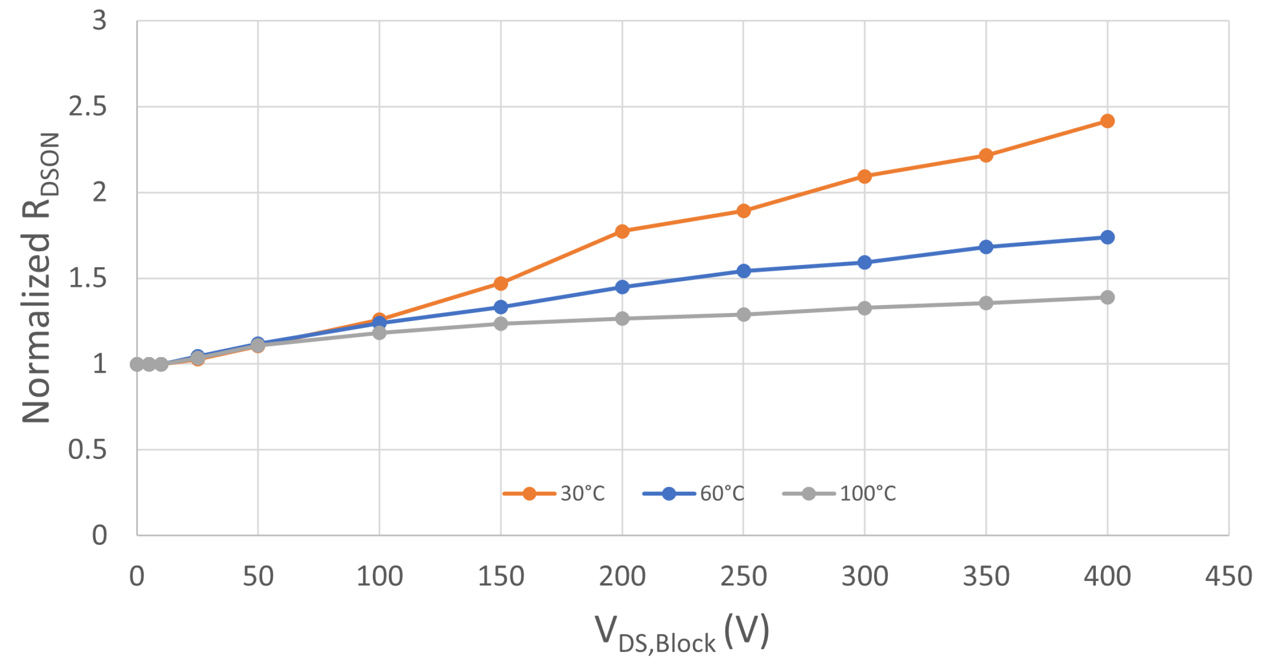
4.2. Dynamic Measurements

The dynamic measurements were carried out following the procedure described before in Figure 1. The measurement period is fixed to 1 ms; indeed, this corresponds to an equivalent application-related switching frequency regime of 1 kHz, and any additional recovery from traps related to higher time constants is of no interest for any practical application. According to the notation of Figure 1, the selected T B l o c k = 500 ns, whereas the entire T O F F = 1.5 μs to include two additional 500 ns dead bands to avoid over-current events. The first test was the sensitivity of R D S , O N to the gate switch-OFF voltage V G S , O F F . Normally ON GaN devices are typically switched off with null or negative V G S . While V G S , O F F = 0 V is suitable for a complete device turn-off, negative values are often used to shorten the commutation time and increase the margin against undesired turn-ON due to the G-D Miller capacitance effect. Nonetheless, negative V G S , O F F values increase the electric fields in the channel during turn-off and can potentially increase trapping with a consequently higher degradation of the dynamic R D S , O N effects. The investigation on the sensitivity towards the sole V G S , O F F was performed by setting the blocking voltage V D S , B l o c k = 0 V at 25 °C. The time domain waveforms of this test are shown in Figure 8.
It is evident that V G S , O F F = 2 V is sufficient to completely switch off the device: the simple event of device switch-off triggers trap-capturing mechanisms that cause a decrease of the drain current, which does not recover completely even after the entire period of 1 ms. Indeed, the asymptotic current value (i.e., I D S , O N in Figure 1) for all the conditions where the device has effectively switched-off (i.e., V G S , O F F = 2 V, 0 V, −3 V) is lower than the reference value with V G S , O F F = 4.8 V. The lower V G S , O F F , the higher the current I D S , O N reduction for fixed V G S , O N , V D S , O N . From the figure it can also be observed that the current recovery is divided into two parts: an initial fast recovery where in 15–20 μs the current reaches about 90% of its asymptotic value and a second slow recovery that lasts for the rest of the 1 ms period. This is an indication of different time constants associated with the de-trapping mechanisms as observed in other studies [16]. As a summary, in Figure 9 the measured degradation of R D S , O N (evaluated at 1 ms) for the three samples and normalized to the nominal case is shown. For this particular technology, still in the early development phase, if the device is switched-off with negative V G S , O F F for better driving performance (increased noise immunity and fast commutation), the conduction performance is worse due to increased trapping effects. V G S , O F F = 0 V is chosen to perform dynamic measurements at variable blocking voltage provided in the following.
The effect of increasing blocking voltages V D S , B l o c k on R D S , O N = 0 V has been investigated varying V D S , B l o c k up to 400 V, which is typically the maximum DC link voltage for a 600 V technology. In Figure 10, the four main characteristics measured by the setup are displayed.
The two different acquisition channels of V D S show significant information during different parts of the period. The increasing blocking voltages during T B l o c k can be evaluated from the acquisition of the isolated voltage probe, whereas the small value of V D S during the rest of the period is acquired by the high accuracy Op-Amp channel and used for the computation of R D S , O N .
It is interesting to observe that the V D S waveform from this latest channel shows the saturation interval of the Op-Amp that lasts only about 2 μs after T B l o c k . Once the Op-Amp exits saturation, an additional 15–18 μs is necessary for the complete extinction of a residual oscillation. Thus, the computation of R D S , O N can be considered completely reliable about 20 μs after the blocking voltage event. Additional minimization of parasitics in the construction of the bench could be implemented to shorten this acquisition delay. From the data in Figure 10, R D S , O N is computed for the entire period and is shown in Figure 11, normalized to the V D S , B l o c k = 0 V case.
The waveforms point out that the trap-activated degradation of the dynamic R D S , O N for this technology under development is very relevant. This effect is already detectable at V D S , B l o c k = 50 V and becomes worse at increasing voltages with R D S , O N reaching up to ×4.5 degradation just after the blocking voltage pulse for the higher V D S , B l o c k = 400 V. In Figure 12, the measured R D S , O N at the end of the ON-state is shown for the three samples as a function of blocking voltage. These data confirm the high degradation levels and the dependence on the applied voltage. Nonetheless, non-negligible differences between samples suggest significant parameter dispersion among devices, another sign of the low level of maturity of the process. The effect of temperature was estimated by measuring the DUT R D S , O N for different chuck temperatures. The R D S , O N measured at the end of the 1 ms period for sample M2 at different chuck temperatures is shown in Figure 13. R D S , O N is normalized to its static value at the corresponding temperature. The plots show that the trap-related degradation effect on R D S , O N decreases for higher temperatures. As observed in [25], this is probably due to the fact that higher temperatures accelerate trap release transients and increase the number of compensating trap release events during T B l o c k . The flexibility of the setup enables setting different parameters according to different requirements. For instance, for trap physical modeling purposes, it could be interesting to evaluate the trap release mechanisms for a longer time frame. The dynamic test at different blocking voltages has been repeated with a much wider period of 40 ms. Figure 14 shows the R D S , O N evolution from 5 ms to 40 ms after T B l o c k : it can be observed that even in a such large time frame the static value of R D S , O N is not reached, indicating that the time constants associated to traps are extremely long.
Another parameter that can be varied is the duration of the blocking voltage application T B l o c k . This parameter is often described in the literature as the duration of the trap-filling pulse. The dependence of the trap-induced degradation to the duration of the trap-filling pulse has been investigated in the literature, sometimes with observed opposite behaviors depending on the duration scale of T B l o c k [15,26,27,28]. For switching mode power converter applications, a dependency of R D S , O N on T B l o c k implies additional dependency of the device performance versus the variation of the duty cycle. Since the target application frequency of this technology is tens to hundreds of KHz, measurements with T B l o c k ranging from 500 ns to 50 μs, while maintaining the same duty cycle, were carried out. These measurements showed practically no dependence of R D S , O N degradation to T B l o c k (in this pulse width variation range).

5. Conclusions

A flexible setup for the characterization of the dynamic R D S , O N of on-wafer high-voltage power transistor has been implemented and used for the characterization of 600 V GaN on Si power switches. The setup enables characterizing the degradation of R D S , O N varying driving voltage, blocking voltage, temperature, and the duration/timing of the applied waveforms, enabling us to explore the degradation of the device performance at different application regimes and also to acquire important information for the process’ physical modeling and optimization. Due to the very limited power dissipation involved in the measurement, the proposed technique can accurately control the DUT temperature without the need for advanced thermal modeling and allows us to apply high voltage excitations compatible with real application scenarios directly on-wafer. The capability to characterize the dynamic R D S , O N of GaN devices directly on wafer before the dicing and packaging of the power transistor is very valuable and time-saving. Therefore, the proposed setup and measurement technique can be useful for foundries during the evolution of a new technology or for quality tests of production wafers. The measurement described in this paper on a new high-voltage GaN technology under development shows the degradation of the dynamic R D S , O N as a function of both the off-state driving voltage V G S , O F F and the V D S blocking voltage V D S , B l o c k . The selection of negative off-state gate voltage is responsible for increased charge trapping that causes degradation of dynamic R D S , O N up to 20–50%. The observed dynamic R D S , O N degradation versus V D S , B l o c k blocking voltages up to 400 V are as relevant as ×4.5 factor increase with respect to its static value. The measurement shows that the time constant associated with de-trapping is in the order of several milliseconds; therefore, the corresponding current recovery does not have any beneficial effect on the dynamic R D S , O N at the application frequencies of interest for this technology (from tens to hundreds of kHz). Finally, it is observed that at increased temperatures the charge recovery is faster and some limited benefit can be observed on the dynamic R D S , O N .

Author Contributions

Conceptualization, C.F., A.A., G.P.G., A.M.A. and A.S.; methodology, A.A., C.F., G.P.G., A.M.A. and A.S.; software, A.A.; validation, A.A. and C.F.; formal analysis, C.F. and A.A.; investigation, A.A. and C.F.; resources, C.F, A.S. and E.S.; data curation, A.A.; writing—original draft preparation, A.A. and C.F.; writing—review and editing, A.A., C.F., G.P.G., A.M.A., A.S. and E.S.; visualization, A.A.; supervision, C.F., A.S. and E.S.; project administration, C.F.; funding acquisition C.F., A.S. and E.S. All authors have read and agreed to the published version of the manuscript.

Funding

This research received no external funding.

Data Availability Statement

The data presented in this study are available in the article.

Conflicts of Interest

The authors declare no conflict of interest.

References

  1. Dimitrijev, S.; Han, J.; Moghadam, H.A.; Aminbeidokhti, A. Power-switching applications beyond silicon: Status and future prospects of SiC and GaN devices. MRS Bull. 2015, 40, 399–405. [Google Scholar] [CrossRef]
  2. Shenai, K.; Dudley, M.; Davis, R.F. Current Status and Emerging Trends in Wide Bandgap (WBG) Semiconductor Power Switching Devices. ECS J. Solid State Sci. Technol. 2013, 2, N3055. [Google Scholar] [CrossRef]
  3. Rupp, R.; Laska, T.; Häberlen, O.; Treu, M. Application specific trade-offs for WBG SiC, GaN and high end Si power switch technologies. In Proceedings of the 2014 IEEE International Electron Devices Meeting, San Francisco, CA, USA, 15–17 December 2014; pp. 2.3.1–2.3.4. [Google Scholar] [CrossRef]
  4. Van Do, T.; Trovão, J.P.F.; Li, K.; Boulon, L. Wide-Bandgap Power Semiconductors for Electric Vehicle Systems: Challenges and Trends. IEEE Veh. Technol. Mag. 2021, 16, 89–98. [Google Scholar] [CrossRef]
  5. Abdelrahman, A.S.; Erdem, Z.; Attia, Y.; Youssef, M.Z. Wide Bandgap Devices in Electric Vehicle Converters: A Performance Survey. Can. J. Electr. Comput. Eng. 2018, 41, 45–54. [Google Scholar] [CrossRef]
  6. He, J.; Zhao, T.; Jing, X.; Demerdash, N.A. Application of wide bandgap devices in renewable energy systems—Benefits and challenges. In Proceedings of the 2014 International Conference on Renewable Energy Research and Application (ICRERA), Milwaukee, WI, USA, 19–22 October 2014; pp. 749–754. [Google Scholar] [CrossRef] [Green Version]
  7. Adan, A.O.; Tanaka, D.; Burgyan, L.; Kakizaki, Y. The Current Status and Trends of 1200-V Commercial Silicon-Carbide MOSFETs: Deep Physical Analysis of Power Transistors From a Designer’s Perspective. IEEE Power Electron. Mag. 2019, 6, 36–47. [Google Scholar] [CrossRef]
  8. She, X.; Huang, A.Q.; Lucia, O.; Ozpineci, B. Review of Silicon Carbide Power Devices and Their Applications. IEEE Trans. Ind. Electron. 2017, 64, 8193–8205. [Google Scholar] [CrossRef]
  9. Nanjo, T.; Imai, A.; Suzuki, Y.; Abe, Y.; Oishi, T.; Suita, M.; Yagyu, E.; Tokuda, Y. AlGaN Channel HEMT with Extremely High Breakdown Voltage. IEEE Trans. Electron Devices 2013, 60, 1046–1053. [Google Scholar] [CrossRef]
  10. Badawi, N.; Hilt, O.; Bahat-Treidel, E.; Böcker, J.; Würfl, J.; Dieckerhoff, S. Investigation of the Dynamic On-State Resistance of 600 V Normally-Off and Normally-On GaN HEMTs. IEEE Trans. Ind. Appl. 2016, 52, 4955–4964. [Google Scholar] [CrossRef]
  11. Systems, G. 650 V E-HEMT GaN TRANSISTORS. 2023. Available online: https://gansystems.com/gan-transistors/gs66516t/ (accessed on 10 January 2023).
  12. STMicroelectronics. G-HEMT 650 V GaN HEMT. 2023. Available online: https://www.st.com/en/power-transistors/g-hemt-650v-gan-hemt.html (accessed on 10 January 2023).
  13. Transphorm. Product Portfolio. 2023. Available online: https://www.transphormusa.com/en/products/ (accessed on 10 January 2023).
  14. Instruments, T. Gallium Nitride (GaN) ICs. 2023. Available online: https://www.ti.com/power-management/gallium-nitride/overview.html (accessed on 10 January 2023).
  15. Angelotti, A.M.; Gibiino, G.P.; Santarelli, A.; Florian, C. Experimental Characterization of Charge Trapping Dynamics in 100-nm AlN/GaN/AlGaN-on-Si HEMTs by Wideband Transient Measurements. IEEE Trans. Electron Devices 2020, 67, 3069–3074. [Google Scholar] [CrossRef]
  16. Angelotti, A.M.; Gibiino, G.P.; Florian, C.; Santarelli, A. Trapping Dynamics in GaN HEMTs for Millimeter-Wave Applications: Measurement-Based Characterization and Technology Comparison. Electronics 2021, 10, 137. [Google Scholar] [CrossRef]
  17. Florian, C.; Cappello, T.; Santarelli, A.; Niessen, D.; Filicori, F.; Popović, Z. A Prepulsing Technique for the Characterization of GaN Power Amplifiers With Dynamic Supply Under Controlled Thermal and Trapping States. IEEE Trans. Microw. Theory Tech. 2017, 65, 5046–5062. [Google Scholar] [CrossRef]
  18. Gibiino, G.P.; Angelotti, A.M.; Santarelli, A.; Florian, C. Microwave Characterization of Trapping Effects in 100-nm GaN-on-Si HEMT Technology. IEEE Microw. Wirel. Compon. Lett. 2019, 29, 604–606. [Google Scholar] [CrossRef]
  19. Yang, S.; Han, S.; Sheng, K.; Chen, K.J. Dynamic On-Resistance in GaN Power Devices: Mechanisms, Characterizations, and Modeling. IEEE J. Emerg. Sel. Top. Power Electron. 2019, 7, 1425–1439. [Google Scholar] [CrossRef]
  20. Wang, H.; Wei, J.; Xie, R.; Liu, C.; Tang, G.; Chen, K.J. Maximizing the Performance of 650-V p-GaN Gate HEMTs: Dynamic RON Characterization and Circuit Design Considerations. IEEE Trans. Power Electron. 2017, 32, 5539–5549. [Google Scholar] [CrossRef]
  21. Barbato, A.; Barbato, M.; Meneghini, M.; Silvestri, M.; Detzel, T.; Haeberlen, O.; Spiazzi, G.; Meneghesso, G.; Zanoni, E. Fast System to measure the dynamic on-resistance of on-wafer 600 V normally off GaN HEMTs in hard-switching application conditions. IET Power Electron. 2020, 13, 2390–2397. [Google Scholar] [CrossRef]
  22. GaN Systems. GSP65RxxHB-EVB 650 V, High Power IMS Evaluation Platform. 2020. Available online: https://gansystems.com/wp-content/uploads/2020/05/GSP65RXXHB-EVB_Technical-Manual_Rev_200526.pdf (accessed on 10 January 2023).
  23. Cappello, T.; Santarelli, A.; Florian, C. Dynamic RON Characterization Technique for the Evaluation of Thermal and Off-State Voltage Stress of GaN Switches. IEEE Trans. Power Electron. 2018, 33, 3386–3398. [Google Scholar] [CrossRef]
  24. De Santi, C.; Meneghini, M.; Meneghesso, G.; Zanoni, E. Review of dynamic effects and reliability of depletion and enhancement GaN HEMTs for power switching applications. IET Power Electron. 2018, 11, 668–674. [Google Scholar] [CrossRef]
  25. Jin, D.; del Alamo, J.A. Methodology for the Study of Dynamic ON-Resistance in High-Voltage GaN Field-Effect Transistors. IEEE Trans. Electron Devices 2013, 60, 3190–3196. [Google Scholar] [CrossRef] [Green Version]
  26. Meneghesso, G.; Meneghini, M.; Silvestri, R.; Vanmeerbeek, P.; Moens, P.; Zanoni, E. High voltage trapping effects in GaN-based metal–insulator–semiconductor transistors. Jpn. J. Appl. Phys. 2015, 55, 01AD04. [Google Scholar] [CrossRef]
  27. Gonçalves, C.F.; Nunes, L.C.; Cabral, P.M.; Pedro, J.C. Pulsed I/V and S-parameters measurement system for isodynamic characterization of power GaN HEMT transistors. Int. J. RF Microw. Comput.-Aided Eng. 2018, 28, e21515. [Google Scholar] [CrossRef]
  28. Gomes, J.L.; Nunes, L.C.; Gonçalves, C.F.; Pedro, J.C. An Accurate Characterization of Capture Time Constants in GaN HEMTs. IEEE Trans. Microw. Theory Tech. 2019, 67, 2465–2474. [Google Scholar] [CrossRef]
Figure 1. Typical waveforms of V G S , V D S , and I D S during the dynamic characterization in periodic regime: waveforms of one period.
Electronics 12 01063 g001
Figure 2. Setting and steps of the proposed measurement procedure under periodic regime.
Electronics 12 01063 g002
Figure 3. Functional simplified description of the setup.
Electronics 12 01063 g003
Figure 4. Schematic of the reconfigurable setup for dynamic R O N measurement.
Electronics 12 01063 g004
Figure 5. Picture of the reconfigurable setup for dynamic R O N measurement in the laboratory.
Electronics 12 01063 g005
Figure 6. Integration of the DUT within the measurement setup. (a) Probe connection to the DUT. (b) Three samples (M1, M2, and M3) are placed on the same metal carrier through epoxy with high electrical and thermal conductivity.
Electronics 12 01063 g006
Figure 7. Static measurements for M1, M2, and M3 samples. (a) Normalized R D S , O N vs. temperature at V G S = 5 V; (b) normalized R D S , O N vs. V G S for ON state.
Electronics 12 01063 g007
Figure 8. V G S (up) and I D S (down) waveforms in case of null blocking voltage at 25 °C. The displayed time interval starts 5 μs before the trigger event and ends 20 μs after the trigger event.
Electronics 12 01063 g008
Figure 9. Normalized R D S , O N vs. V g s , O F F for M1, M2, and M3 samples.
Electronics 12 01063 g009
Figure 10. V G S , I D S , and V D S (from isolated voltage probe and Op-Amp) acquired waveforms for R D S , O N calculation at increasing blocking voltage. The displayed time interval starts 5 μs before the trigger event and ends 20 μs after the trigger event.
Electronics 12 01063 g010
Figure 11. Normalized R D S , O N of a single sample measured over the entire ON-time.
Electronics 12 01063 g011
Figure 12. Normalized R D S , O N evaluated at the end of ON-time for the M1, M2, and M3 samples.
Electronics 12 01063 g012
Figure 13. Normalized R D S , O N vs. V b l o c k of sample M2 for three temperatures: 30 °C, 60 °C, and 100 °C.
Electronics 12 01063 g013
Figure 14. Normalized R D S , O N vs. V D S , B l o c k with an extended 40 ms period to evaluate the traps’ long time constants.
Electronics 12 01063 g014
Table 1. DUT preliminary electrical specifications.
V BD V gs V th R DS C ISS   1 C OSS   1 C RSS   1
600 V5–6 V2–2.5 V0.5 Ω43 pF18 pF1 pF
1 VDS = 200 V.
Disclaimer/Publisher’s Note: The statements, opinions and data contained in all publications are solely those of the individual author(s) and contributor(s) and not of MDPI and/or the editor(s). MDPI and/or the editor(s) disclaim responsibility for any injury to people or property resulting from any ideas, methods, instructions or products referred to in the content.

