
A Basic Design Tool for Grid-Connected AC–DC Converters Using Silcon Carbide MOSFETs

Abstract
:1. Introduction
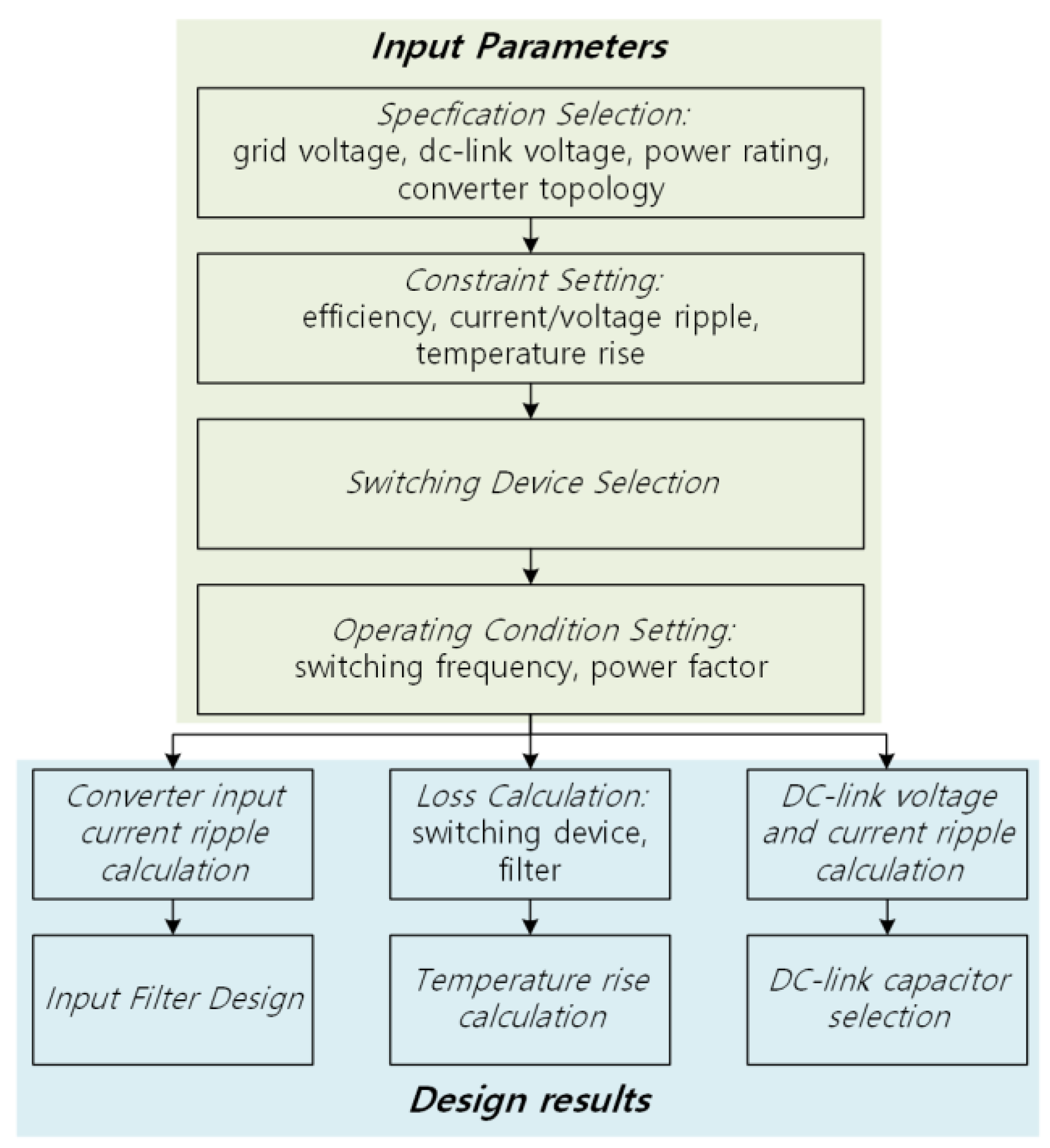
2. Design Procedures
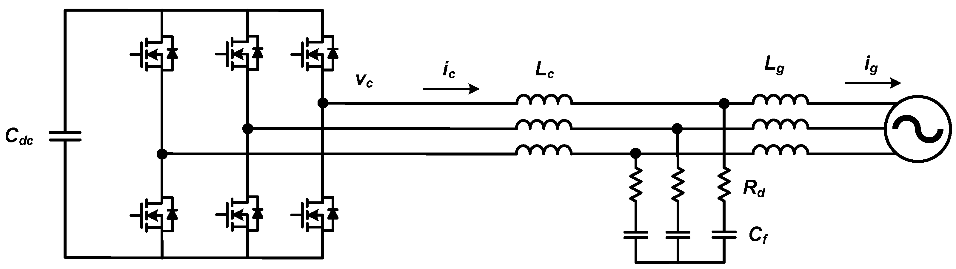
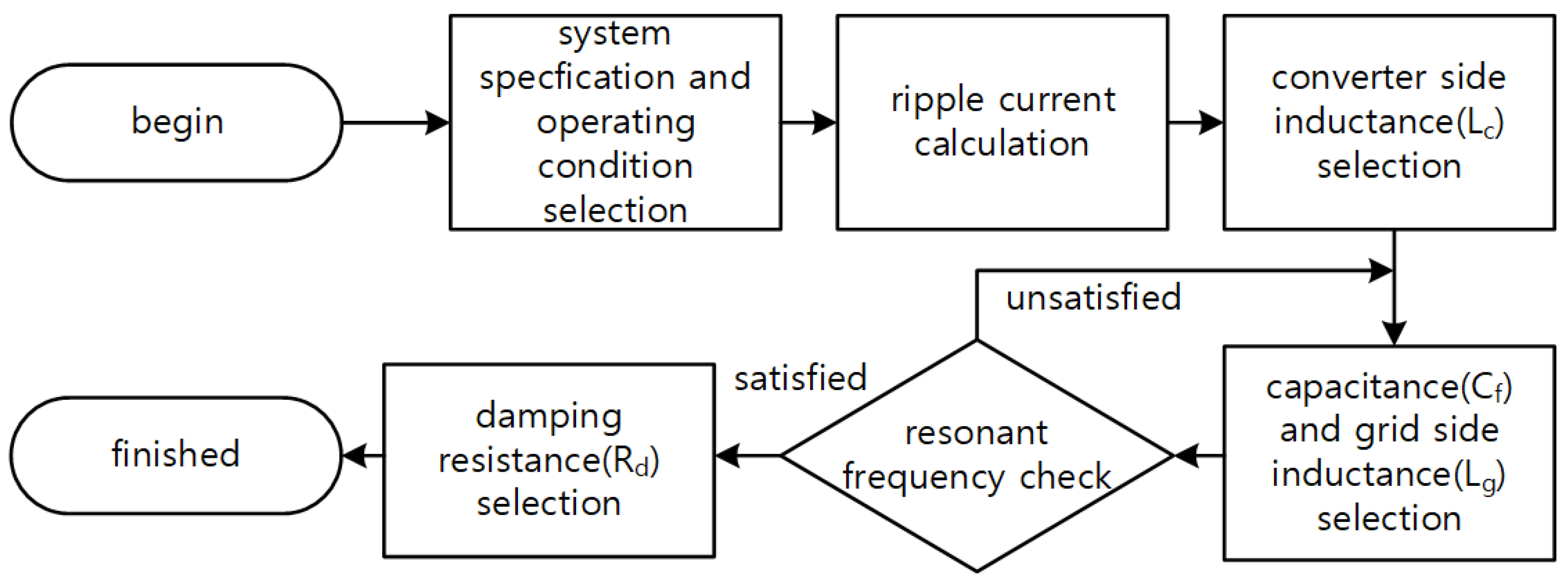
2.1. Input Filter Design Procedure
- Select system specifications and operating conditions:Select the grid voltage, grid frequency, converter type (2L or 3L-NPC), switching frequency, DC-link voltage, and rated current.
- Calculate ripple current and select converter side inductance:Set the converter-side ripple current limit. Select the limit value of the peak-to-peak amplitude of the current ripple relative to the rated current and calculate the converter-side inductor value that satisfies the ripple current according to the operating conditions. The peak-to-peak amplitude of the ripple current generated by the converter is determined by the operating conditions, and the instantaneous phase angle and can be expressed as (2) [18].where Vdc is the DC-link voltage, Ts is the switching period, and r(m,θ) is a function of the voltage modulation index (m) and the output voltage phase angle (θ). The magnitude of the instantaneous current ripple depends on the phase angle, but the proposed method calculates the magnitude of the current ripple based on the output voltage at a phase angle of 90°. In general, the power factor of a grid-connected converter is close to unity, so the output voltage and current are almost in-phase, and the magnitude of the current flowing in the converter is maximized around 90 degrees. Therefore, when considering the maximum current flowing through the converter due to current ripple, it is appropriate to base the design on the value when the phase angle is 90°. The converter-side inductance (Lc) value that satisfies the magnitude of the ripple current can be selected by using (2).
- Select capacitance and grid-side inductance:The larger the capacitor of the LCL filter, the better it can absorb the converter’s ripple current and reduce the harmonics of the grid-side current. However, the capacitor in the input filter introduces reactive power at the grid side and changes the grid side power factor. Typically, the reactive power flowing into the capacitor is limited to 2–5% of the apparent power in the design of the input filter [19]. The proposed design tool takes the reactive power value of the capacitor as input and selects the capacitor divisor of the corresponding filter. The formula for selecting the capacitance value is shown in (3).where S is the apparent power of the converter, ω is the frequency of the grid, Vph is the phase voltage of the grid, and R is the ratio of the reactive power to the apparent power. In studies dealing with LCL filter design, the values of the grid-side inductance and the converter-side inductance are often chosen to be equal. This is because, when the resonant frequency of the LCL filter is first determined, equalizing the two inductance values results in the smallest magnitude of the total inductance [20], i.e., the harmonics of the grid current can be reduced the most with the same inductance value. However, in this paper, the filter is designed based on the ripple current on the converter side, not the current harmonics delivered to the grid. In the case of converters using SiC MOSFETs, the low-order harmonics that contribute most to the grid current harmonics can be significantly suppressed by current controllers, so the proposed method focuses more on the converter-side inductor in the total inductance used in the input filter. In this paper, the grid-side inductance is selected as one-third of the converter-side inductance.
- Check the resonant frequency of the input filter:The resonant frequency (fres) of the input filter should be less than one-half of the sampling frequency (fs) according to the Nyquist sampling theory, and it should be higher than the bandwidth (fb) of the current controller to avoid affecting the current control behavior [21].Finally, check whether the parameters of the input filter selected satisfies (4), and if not, adjust the capacitance value so that the resonant frequency satisfy the limitation of (4).
- Select damping resistor:The LCL filter theoretically has zero impedance at its resonant frequency. The damping resistor is used to provide impedance at this time to suppress the oscillation of the current at the resonant frequency. For this purpose, the value of the damping resistor is designed to be similar to the impedance of the capacitor connected in series at the resonant frequency [22], and in this paper, it is selected as one-third of the impedance of the capacitor at the resonant frequency.
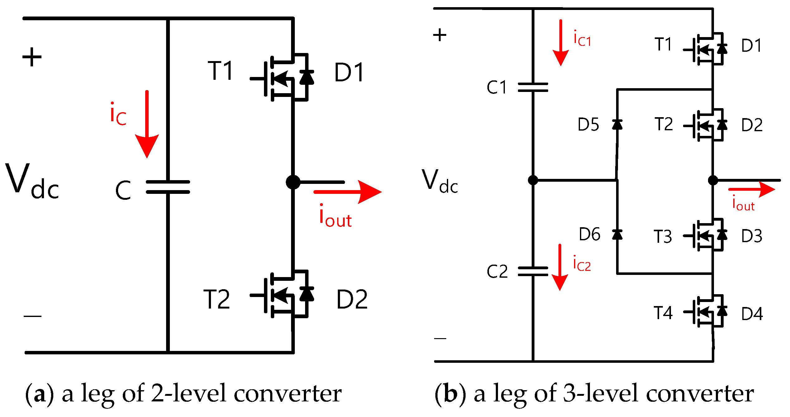
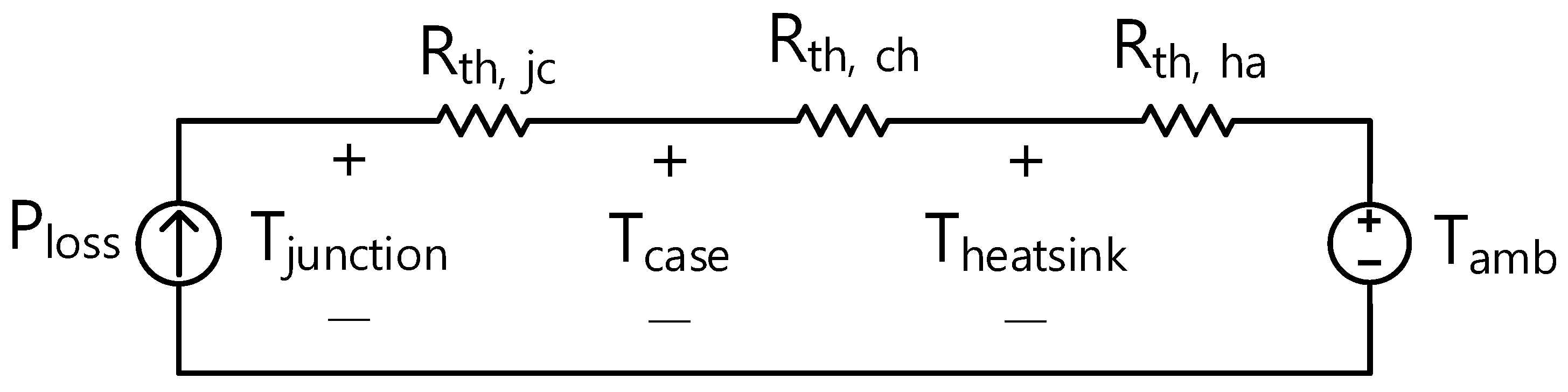
2.2. Calculating Losses and Temperature Rise
2.3. DC-Link Voltage, Current Ripple Calculations
3. Design Examples
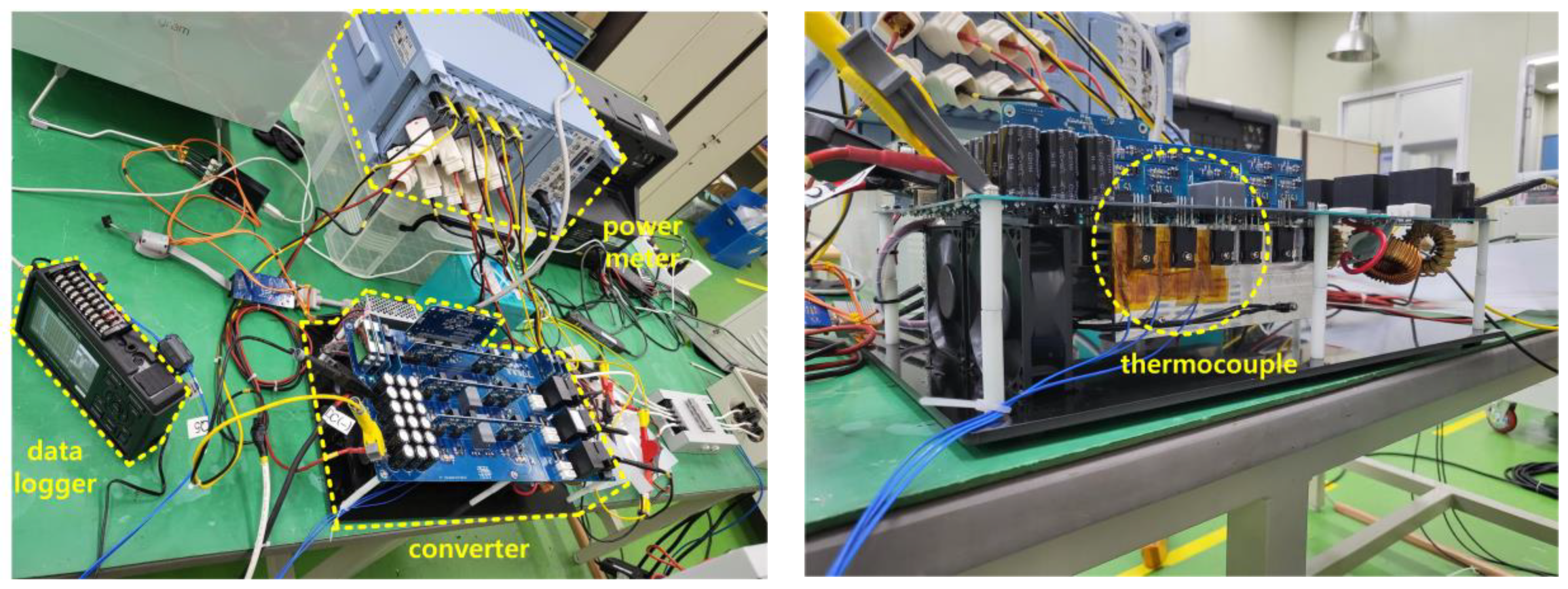
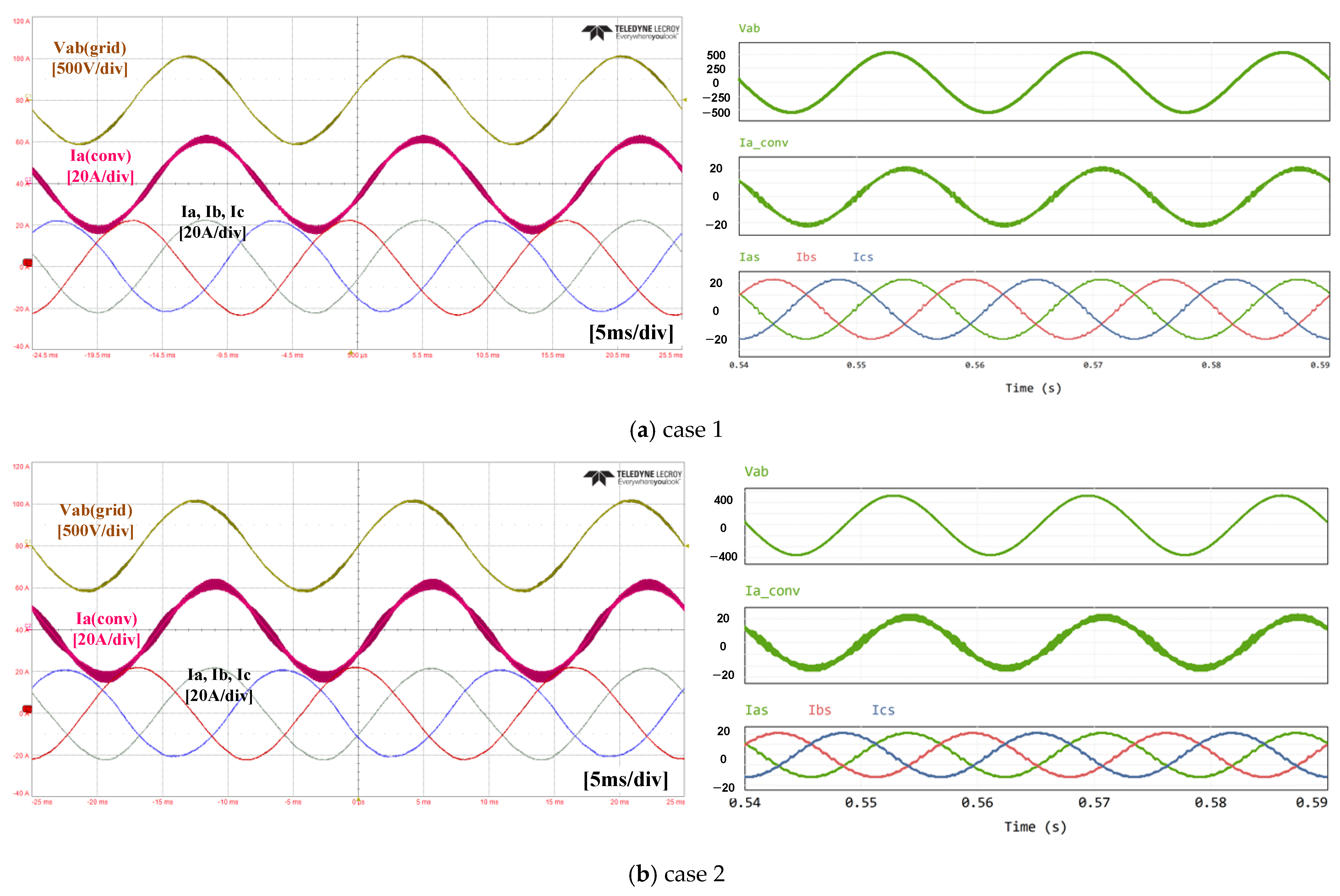
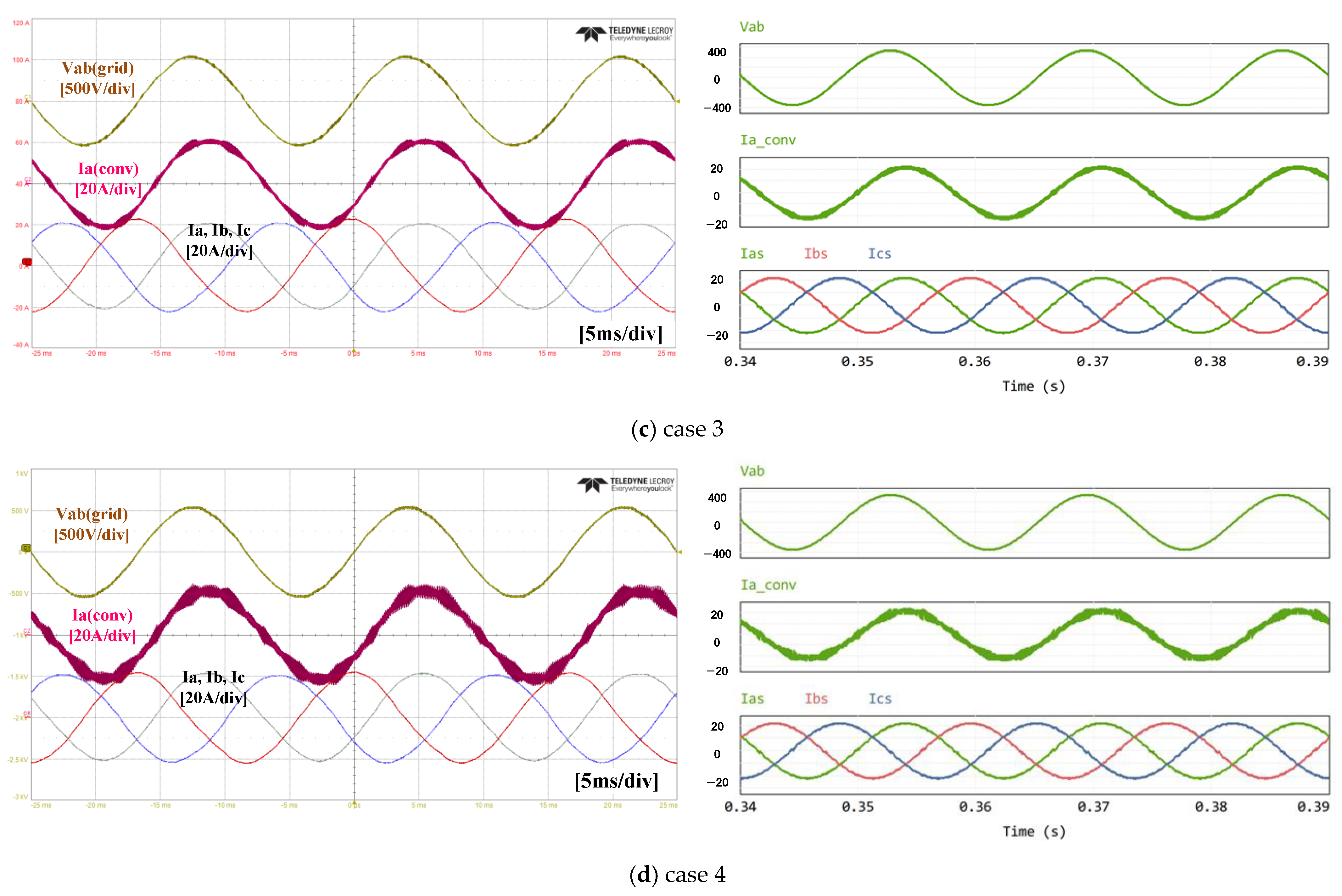
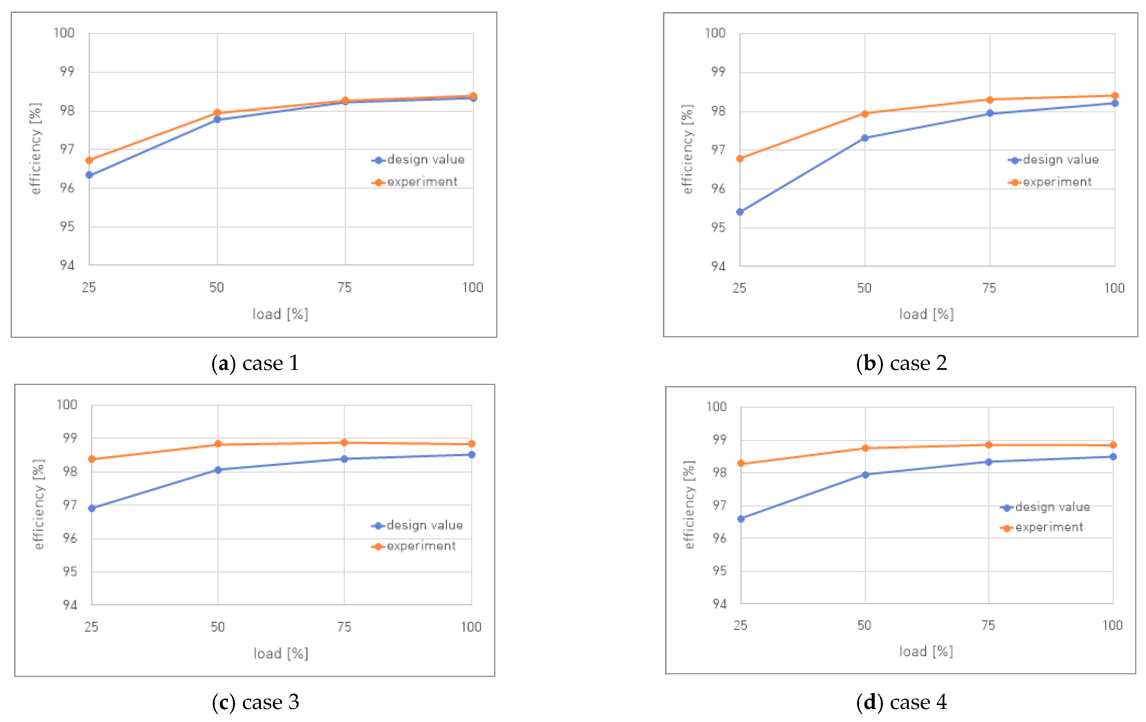
4. Simulation and Experimental Results
5. Conclusions
Author Contributions
Funding
Data Availability Statement
Conflicts of Interest
References
- Mohan, N.; Undeland, T.M.; Robbins, W.P. Power Electronics: Converters, Applications, and Design; Wiley: Hoboken, NJ, USA, 2003. [Google Scholar]
- Rashid, M.H. Power Electronics: Circuits, Devices, and Applications; Pearson: London, UK, 2011. [Google Scholar]
- Erickson, R.W.; Maksimović, D. Fundamentals of Power Electronics; Springer: Berlin/Heidelberg, Germany, 2007. [Google Scholar]
- Toshon, T.A.; Faruque, M.O. A design optimisation tool to minimise volume and failure rate of the modular multilevel converter and the thyristor-controlled rectifier. J. Mar. Eng. Technol. 2023, 22, 189–198. [Google Scholar] [CrossRef]
- Saha, J.; Hazarika, D.; Gorla, N.B.Y.; Panda, S.K. Machine-Learning-Aided Optimization Framework for Design of Medium-Voltage Grid-Connected Solid-State Transformers. IEEE J. Emerg. Sel. Top. Power Electron. 2021, 9, 6886–6900. [Google Scholar] [CrossRef]
- Soeiro, T.B.; Mühlethaler, J.; Linnér, J.; Ranstad, P.; Kolar, J.W. Automated Design of a High-Power High-Frequency LCC Resonant Converter for Electrostatic Precipitators. IEEE Trans. Ind. Electron. 2013, 60, 4805–4819. [Google Scholar] [CrossRef]
- Liu, X.; Qiu, L.; Fang, Y.; Wang, K.; Li, Y.; Rodríguez, J. Finite Control-Set Learning Predictive Control for Power Converters. IEEE Trans. Ind. Electron. 2023. [Google Scholar] [CrossRef]
- Liu, X.; Qiu, L.; Fang, Y.; Wang, K.; Li, Y.; Rodríguez, J. Predictive Control of Voltage Source Inverter: An Online Reinforcement Learning Solution. IEEE Trans. Ind. Electron. 2023. [Google Scholar] [CrossRef]
- Li, X.; Zhang, X.; Lin, F.; Blaabjerg, F. Artificial-Intelligence-Based Design for Circuit Parameters of Power Converters. IEEE Trans. Ind. Electron. 2022, 69, 11144–11155. [Google Scholar] [CrossRef]
- Dragičević, T.; Wheeler, P.; Blaabjerg, F. Artificial Intelligence Aided Automated Design for Reliability of Power Electronic Systems. IEEE Trans. Power Electron. 2019, 34, 7161–7171. [Google Scholar] [CrossRef]
- WEBENCH Circuit Designer. Available online: https://www.ti.com/tool/WEBENCH-CIRCUIT-DESIGNER (accessed on 13 October 2023).
- SMPS Designer. Available online: https://infineon.poweresim.com/ (accessed on 13 October 2023).
- The General Converter Design Tool. Available online: https://wbg.koema.or.kr (accessed on 13 October 2023).
- Holmes, D.G.; Lipo, T.A. Pulse Width Modulation for Power Converters: Principles and Practice; IEEE Press: Piscataway, NJ, USA, 2003. [Google Scholar]
- IEEE Standard 519-2014; IEEE Recommended Practices and Requirements for Harmonic Control in Electrical Power Systems, (Revision of IEEE Standard 519-1992). IEEE: New York, NY, USA, 2014; pp. 1–29. [CrossRef]
- IEEE Standard 1547-2018; IEEE Standard for Interconnection and Interoperability of Distributed Energy Resources with Associated Electric Power Systems Interfaces, (Revision of IEEE Std 1547-2003). IEEE: New York, NY, USA, 2018. [CrossRef]
- Lascu, C.; Asiminoaei, L.; Boldea, I.; Blaabjerg, F. Frequency Response Analysis of Current Controllers for Selective Harmonic Compensation in Active Power Filters. IEEE Trans. Ind. Electron. 2009, 56, 337–347. [Google Scholar] [CrossRef]
- Grandi, G.; Loncarski, J.; Dordevic, O. Analysis and Comparison of Peak-to-Peak Current Ripple in Two-Level and Multilevel PWM Inverters. IEEE Trans. Ind. Electron. 2015, 62, 2721–2730. [Google Scholar] [CrossRef]
- Jiao, Y.; Lee, F.C. LCL Filter Design and Inductor Current Ripple Analysis for a Three-Level NPC Grid Interface Converter. IEEE Trans. Power Electron. 2015, 30, 4659–4668. [Google Scholar] [CrossRef]
- Jalili, K.; Bernet, S. Design of LCL filters of active-front-end two level voltage-source converters. IEEE Trans. Ind. Electron. 2009, 56, 1674–1689. [Google Scholar] [CrossRef]
- Jayalath, S.; Hanif, M. Generalized LCL-Filter Design Algorithm for Grid-Connected Voltage-Source Inverter. IEEE Trans. Ind. Electron 2017, 64, 1905–1915. [Google Scholar] [CrossRef]
- Liserre, M.; Blaabjerg, F.; Hansen, S. Design and control of an LCL-filter-based three-phase active rectifier. IEEE Trans. Ind. Appl. 2005, 41, 1281–1291. [Google Scholar] [CrossRef]
- Górecki, P. Electrothermal Averaged Model of a Diode–IGBT Switch for a Fast Analysis of DC–DC Converters. IEEE Trans. Power Electron. 2022, 37, 13003–13013. [Google Scholar] [CrossRef]
- Górecki, P.; Górecki, K. Measurements and computations of internal temperatures of the IGBT and the diode situated in the common case. Electronics 2021, 10, 210. [Google Scholar] [CrossRef]
- KVenkatachalam; Sullivan, C.R.; Abdallah, T.; Tacca, H. Accurate prediction of ferrite core loss with nonsinusoidal waveforms using only Steinmetz parameters. In Proceedings of the Computers in Power Electronics, Mayaguez, PR, USA, 3–4 June 2002; pp. 36–41. [Google Scholar]
- Karanayil, B.; Agelidis, V.G.; Pou, J. Performance Evaluation of Three-Phase Grid-Connected Photovoltaic Inverters Using Electrolytic or Polypropylene Film Capacitors. IEEE Trans. Sustain. Energy 2014, 5, 1297–1306. [Google Scholar] [CrossRef]
- Zhao, Z.; Diao, F.; Wu, Y.; Wang, Z.; Zhao, Y. DC-Link Capacitor Current Modeling and Analysis for Three-Level Voltage Source Inverters. In Proceedings of the IEEE Applied Power Electronics Conference and Exposition (APEC), Phoenix, AZ, USA, 14–17 June 2021. [Google Scholar]
- Jiang, D.; Wang, F. Current-Ripple Prediction for Three-Phase PWM Converters. IEEE Trans. Ind. Appl. 2014, 50, 531–538. [Google Scholar] [CrossRef]


| Maximum Harmonic Current Distortion in Percent of IL | ||||||
|---|---|---|---|---|---|---|
| Individual Harmonic Order (Odd Harmonics) a,b | ||||||
| ISC/IL | 3 ≤ h < 11 | 11 ≤ h < 17 | 17 ≤ h < 23 | 23 ≤ h < 35 | 35 ≤ h ≤ 50 | TDD |
| <20 c | 4.0 | 2.0 | 1.5 | 0.6 | 0.3 | 5.0 |
| 20 < 50 | 7.0 | 3.5 | 2.5 | 1.0 | 0.5 | 8.0 |
| 50 < 100 | 10.0 | 4.5 | 4.0 | 1.5 | 0.7 | 12.0 |
| 100 < 1000 | 12.0 | 5.5 | 5.0 | 2.0 | 1.0 | 15.0 |
| >1000 | 15.0 | 7.0 | 6.0 | 2.5 | 1.4 | 20.0 |
| Individual Odd Harmonic Order, h | h < 11 | 11 ≤ h < 17 | 17 ≤ h < 23 | 23 ≤ h < 35 | 35 ≤ h < 50 | Total Rated Current Distortion (TRD) |
|---|---|---|---|---|---|---|
| Percent (%) | 4.0 | 2.0 | 1.5 | 0.6 | 0.3 | 5.0 |
| Individual Even Harmonic Order, h | h = 2 | h = 4 | h = 6 | 8 ≤ h < 50 |
|---|---|---|---|---|
| Percent (%) | 1.0 | 2.0 | 3.0 | Associated range specified in Table 2 |
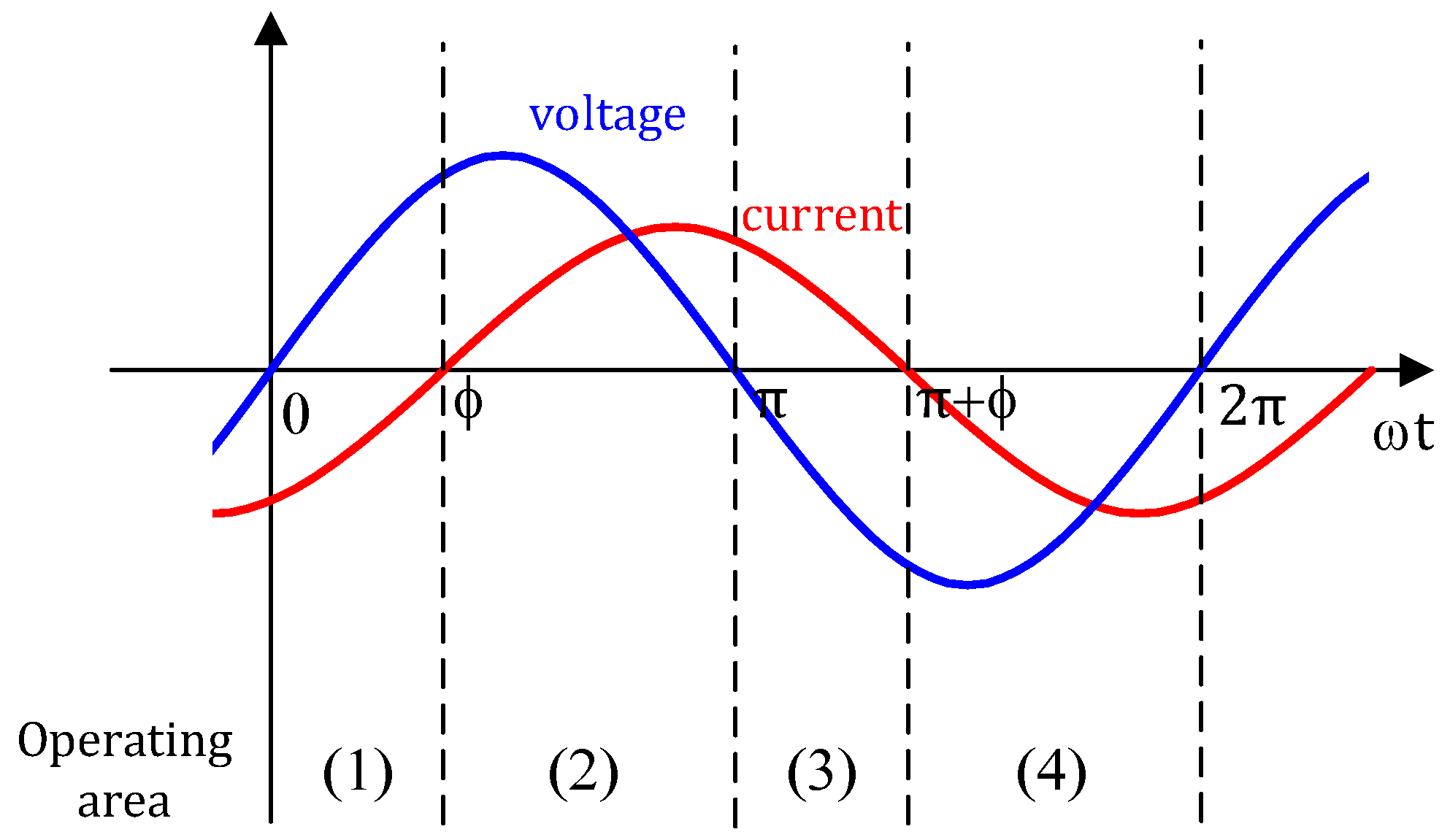
| Operating Area | (1) | (2) | (3) | (4) | |
|---|---|---|---|---|---|
| 2L | conduction path | T1 or T2 | |||
| switching loss | T2 | T1 | T2 | ||
| 3L-NPC | conduction path | T1, T2 or T3, D6 | T1, T2 or D5, T2 | D5, T2 or T3, T4 | T3, T4 or T3, D6 |
| switching loss | T3 | T1 | T2 | T4 | |
| conduction loss | T1, T2 | |
| switching loss | T1, T2 |
| conduction loss | T1, T4 | |
| T2, T3 | ||
| D5, D6 | ||
| switching loss | T1, T4 | |
| T2, T3 |
| ma | β | A | B | C | D |
|---|---|---|---|---|---|
| - | 1 | 0 | 0 | ||
| Case 1 | Case 2 | Case 3 | Case 4 | |
|---|---|---|---|---|
| topology | 2L | 2L | 3L-NPC | 3L-NPC |
| capacity [kVA] | 10 | 10 | 10 | 10 |
| power factor | 0.99 | 0.99 | 0.99 | 0.99 |
| input voltage/ dc-link voltage [V] | 380/740 | 380/740 | 380/740 | 380/740 |
| power semiconductor | C3M0032120K | C3M0032120K | C3M0060065K, E3D30065D | C3M0060065K, E3D30065D |
| switching frequency [kHz] | 50 | 50 | 50 | 50 |
| current ripple ratio [%] | 22 | 33 | 10 | 20 |
| voltage ripple ratio [%] | 1 | 1 | 1 | 1 |
| Case 1 | Case 2 | Case 3 | Case 4 | |
|---|---|---|---|---|
| converter side inductance (Lc) [μH] | 387 | 258 | 194 | 97 |
| grid side inductance (Lc) [μH] | 129 | 86 | 65 | 32 |
| filter capacitance (Cf) [μF] | 6.1 | 6.1 | 6.1 | 6.1 |
| damping resistance (Rd) [Ω] | 1.3 | 1 | 2 | 1.3 |
| minimum dc-link capacitance [μF]/[A] | 7.9/9.2 | 7.9/9.2 | 6.2/7.3 | 6.2/7.3 |
| Case 1 | Case 2 | Case 3 | Case 4 | ||
|---|---|---|---|---|---|
| current ripple [A] | design value | 4.8 | 7.2 | 2.2 | 4.3 |
| experimental results | 4.0 | 7.1 | 2.8 | 5.6 | |
| THD [%] | experimental results | 2.44 | 2.4 | 2.7 | 2.3 |
| temperature rise [K] | design value | 14.2 | 14.2 | 12.7 | 12.7 |
| experimental results | 13.7 | 14.2 | 8.5 | 10.7 | |
Disclaimer/Publisher’s Note: The statements, opinions and data contained in all publications are solely those of the individual author(s) and contributor(s) and not of MDPI and/or the editor(s). MDPI and/or the editor(s) disclaim responsibility for any injury to people or property resulting from any ideas, methods, instructions or products referred to in the content. |
© 2023 by the authors. Licensee MDPI, Basel, Switzerland. This article is an open access article distributed under the terms and conditions of the Creative Commons Attribution (CC BY) license (https://creativecommons.org/licenses/by/4.0/).
Share and Cite
Kim, M.; Yun, H.-J. A Basic Design Tool for Grid-Connected AC–DC Converters Using Silcon Carbide MOSFETs. Electronics 2023, 12, 4828. https://doi.org/10.3390/electronics12234828
Kim M, Yun H-J. A Basic Design Tool for Grid-Connected AC–DC Converters Using Silcon Carbide MOSFETs. Electronics. 2023; 12(23):4828. https://doi.org/10.3390/electronics12234828
Chicago/Turabian StyleKim, Myoungho, and Hyeok-Jin Yun. 2023. "A Basic Design Tool for Grid-Connected AC–DC Converters Using Silcon Carbide MOSFETs" Electronics 12, no. 23: 4828. https://doi.org/10.3390/electronics12234828