Article

Design of Power Supply Based on Inductive Power Transfer System for Medium Voltage Direct Current Sensor

1
Department of Electrical Engineering, Chonnam National University, 77, Yongbong-ro, Buk-gu, Gwangju 61186, Republic of Korea
2
Energy Convergence Research Center, Korea Electronics Technology Institute, 226, Cheomdangwagi-ro, Buk-gu, Gwangju 61011, Republic of Korea
*
Authors to whom correspondence should be addressed.
Electronics 2023, 12(22), 4702; https://doi.org/10.3390/electronics12224702
Submission received: 7 September 2023 / Revised: 15 November 2023 / Accepted: 17 November 2023 / Published: 19 November 2023

Abstract

:
This paper proposes a medium voltage direct current (MVDC) sensor power supply method based on inductive power transfer (IPT). Given that MVDC distribution networks transmit power at high voltages (several tens of kV), control through sensors is necessary to prevent exacerbating MVDC distribution network accidents. Moreover, these high voltages in MVDC distribution networks mean that high voltage insulation is required between the sensor and the distribution line and for any power supply device electrically connected to the sensor. Therefore, this paper proposes a safe and reliable power supply method using the principle of IPT to maintain a suitable insulation distance between the distribution network and the current sensor supply line. After proposing and designing a transmitter/receiver pad and IPT system by considering the current sensor specifications, a 50-W experimental prototype is developed. The experiments demonstrated that the proposed IPT system can resolve concerns about the breakdown of insulation between distribution networks and power supply lines.

1. Introduction

Medium voltage direct current (MVDC) technology is a transmission and conversion technology with a voltage level of 1.5–100 kV and a high-power transmission capacity for intermediate connections between high voltage DC (HVDC) and low voltage DC (LVDC) technologies applied to DC power transmission systems [1,2,3]. MVDC has been regarded as an effective solution to the problem of unstable power supplies caused by the expansion of renewable energy sources, DC demand for data centers, ESSs, and electric vehicles [4,5]. Accordingly, extensive research has been conducted on transmitting and distributing high voltages and power, as displayed in Figure 1. Furthermore, research on the commercialization of MVDC is proceeding, mainly due to recent technological advances in power semiconductor devices and real-time controllers [6,7,8].
Protective devices and accident detection circuits are required to prevent any increase in the severity of grid accidents when operating MVDC distribution networks. Currently, smart sensors and intelligent electronics (IEDs) detect and respond to power device failures by measuring and analyzing voltage and current signals on the MVDC distribution lines [9,10,11]. However, when attaching a control sensor to a distribution line, a high voltage insulation level is required to prevent any breakdown of the distribution line insulation. Moreover, any auxiliary power for the control circuit should also have a high voltage insulation level.
This paper proposes the concept of introducing wireless power transfer (WPT) methods for supplying high-voltage insulated auxiliary power supply to MVDC current/voltage instruments. The WPT system solves the problems of dust and leakage current due to cable aging and has the advantage of electrical insulation because there is an air gap in the path that transmits power from the supply source to the load (instead of copper wires) [12,13].
The remainder of this paper is structured as follows: Section 2 presents the basic operating principles of the proposed wireless power supply and the specifications of the power supply, after which the most suitable wireless charging method is selected. Section 3 presents the design process after selecting the wireless charging method, while the simulation and experimental results are provided and analyzed in Section 4. Section 5 presents the conclusions.

2. Basic Analysis of Wireless Power Transfer System

2.1. Description of Wireless Power Transfer System Type and Selection of Transmission Method

There are four types of WPT systems: inductive power transfer (IPT), which transmits power from the transmitter coil to the receiver coil via electromagnetic induction; microwave power transfer (MPT), which uses microwaves; laser power transfer (LPT), which uses lasers; and capacitive power transfer (CPT) systems, which use the principle of a capacitor. Descriptions of the characteristics of each WPT method are presented in Table 1.
The IPT system can transmit power over distances from several to tens of centimeters, can supply power (MW) at a high efficiency of more than 90%, and can operate at frequencies of tens to hundreds of kHz. Hence, the performance of power semiconductors required by other WPT platforms is relatively low [14,15,16]. MPT has the advantage of being able to transmit power over distances of up to several kilometers. However, the transmission and reception antennas are very large, inefficient, present human hazards, and require high-performance power semiconductors due to the high GHz operating frequencies [17]. LPT also has the advantage of being able to transmit power up to several kilometers. However, the efficiency and transmission power are low, and the charging efficiency decreases rapidly when there is a separation distance to the receiving pad [18,19,20,21]. CPT is similar to the IPT system by using an aluminum plate as a single capacitor. However, unlike magnetic induction, which can increase inductance values when manufactured in flat plate form, CPT requires high-frequency operation (hundreds of kHz to several MHz) [22,23,24]. Therefore, considering the specifications in Table 1 and the preceding discussion, the IPT method was selected for the proposed power supply.

2.2. Analysis of Electrical and Environmental Conditions of Auxiliary Power Supply

Before designing the IPT system, the specification of the power supply device applied to the MVDC current sensor was analyzed. Both electrical and environmental conditions should be considered prior to designing an auxiliary power supply using the WPT system. First, the electrical isolation distance between the MVDC and the auxiliary power supply should be determined. Generally, when insulating through air, a separation distance of 3 [kV/mm] must be set based on DC [25]. In addition, the separation distance should be selected in consideration of the decrease in air insulation voltage and the separation of distribution lines due to natural disasters. In this paper, the MVDC voltage level required for insulation could be up to 69 kV and should have a minimum separation distance of 23 mm. Moreover, considering that the insulation voltage of air can vary depending on a range of factors (such as the weather, humidity, and vibrations), the minimum separation distance was assumed to be 30 mm.
After selecting the separation distance range for air insulation, the geometric specifications of the wireless pad were considered. Figure 2 presents the basic specification of an MVDC class voltage/current sensor. The side and bottom surfaces of the sensor drawing can be used, and a large floor surface was used in this study. With respect to the sensor enclosure, the maximum available volume for the receiver pad is 94 mm wide, 141.5 mm long, and 15–20 mm inner height. The proposed IPT system was configured in consideration of these conditions.
Finally, the range of output characteristics should be considered, which can fluctuate according to the separation distance. Since a regulator is attached to the output stage of the IPT converter to supply a certain rated voltage, the variable input voltage range required by the regulator should be satisfied. The input voltage required by the regulator is 15–50 V and the rated power is 50 W, and the output voltage/current should be achieved even when the separation distance fluctuates. The basic conditions required for supplying auxiliary power in an IPT system are specified in Table 2.

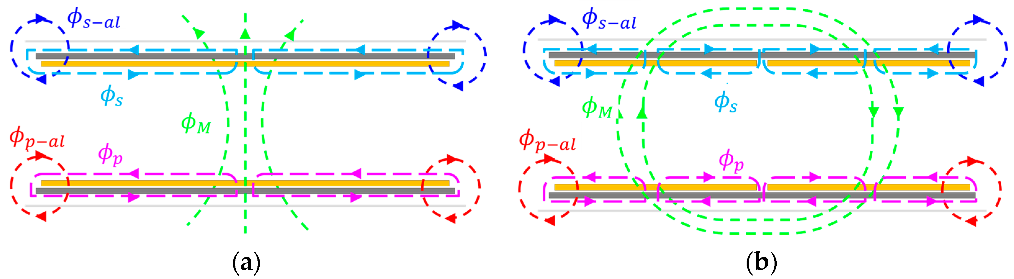
2.3. Basic Analysis of Inductive Power Transfer System

Figure 3 displays the configuration of an IPT converter. The entire system consists of an inverter that converts DC power to AC, a transmitter/receiver pad that transmits power using electromagnetic induction, a transmitter/receiver resonance circuit that compensates for pad reactance to achieve high-frequency operation, a rectifier that rectifies AC power to DC, and voltage regulator that converts an input variable voltage into constant output. A typical IPT converter creates an AC voltage with the operating frequency required by the IPT system using a half-bridge consisting of two MOSFETs of a full-bridge inverter (which contains four MOSFETs). The input AC voltage is a square wave voltage configured with a fixed duty of 0.5. This square wave includes various harmonics in the basic switching frequency waveform. However, since the resonance circuits that constitute the IPT converter act as harmonic filters, only the basic frequency waveform is transmitted to the output side and the harmonics can be neglected. Accordingly, the inverter output voltage waveform can be approximated by Equation (1) including only the fundamental frequency. In the case of a half-bridge inverter, m = 1 is used, whereas m = 2 is used in the case of a full-bridge inverter.
U i n = 2 m U D C π 2 ( m = 1 , 2 ) .
The AC power is transmitted through the wireless pad. The transmitter and receiver pads comprise pad inductance (Li) and parasitic resistance components Ri (where i = p, s) that are dependent on the skin effect. The total wireless pad resistance is determined by the sum of the DC resistance, the skin effect, and the proximity effect. M is the mutual inductance between the transceiver coils, and the coupling coefficient (k) is defined as follows:
k = M L p L s .
The AC power transmitted through the wireless pad is converted to DC through a rectifier and a filter capacitor. The rectifier typically uses a single-phase full bridge rectifier consisting of four power diodes. The load-side voltage (UL) and current (IL) can be expressed as an AC equivalent circuit:
U L = π 2 4 U o , a c ,   I L = π 2 2 i o , a c .
From Equation (3), the AC equivalent resistance is as follows:
R o , a c = π 2 8 R L .
Through Equations (1), (3), and (4), the inverter and the full bridge rectifier can be replaced by a sinusoidal voltage source and an AC equivalent resistance. Figure 4 presents the IPT converter AC equivalent circuit based on the network current method. Equation (5) expresses the network current method as a matrix equation, and Equation (7) is an impedance equation composed of mutual inductances.
[ U i n U o , a c ] = [ Z 11 Z 12 Z 21 Z 22 ] [ i i n i o , a c ] .
Z 12 = Z 21 = j ω M .
Since the calculation formula changes according to the resonant network configured, the details of the detailed formula can be confirmed during the subsequent compensation topology selection process.

3. Design Steps of Inductive Power Transfer System and Design Conditions for Auxiliary Power for MVDC Class Current and Voltage Sensors

This section presents a description of the process of fabricating an IPT system based on the analysis results provided in Section 2. The IPT system is established by selecting the pad design, compensation topology, and operating frequency.

3.1. Design of Wireless Pad

The change in the value of k between the transmitter and receiver pad results in a change in M. Therefore, it is important to minimize the variation in k due to fluctuations in the separation distance. Depending on the coil winding method, the types of wireless pads include a circular pad (CP), a rectangular pad (RP), a double-D pad (DDP), a bipolar pad (BPP), and a double-D quadrature pad (DDQP). The CP and RP have unipolar magnetic flux paths, while the DDP, BPP, and DDQP have bipolar magnetic flux paths. Figure 5 presents the magnetic flux paths for the CP and DDP. Wireless pads with unidirectional magnetic flux paths (such as CPs) have a constant decrease in k in all directions when the separation distance fluctuates. Wireless pads with bidirectional magnetic flux paths (such as DDPs) have different k fluctuations (even with separation distance fluctuations), depending on the formation of magnetic flux paths. Terms ϕp and ϕs are the transmitter and receiver magnetic fluxes, respectively, while ϕp-al and ϕs-al are the leakage magnetic fluxes, and ϕM is the mutual magnetic flux. Figure 6 presents a finite element method (FEM) simulation configuration of a CP with a single magnetic flux path and a DDP with a bidirectional magnetic flux path. The coil consists of 20 turns for the transmitter and 13 turns for the receiver.
After configuring the wireless pad for the simulation, the results of k according to the separation distance were compared. Figure 7 displays the results of k according to separation distance using the FEM simulation. The vertical separation distance was tested from 30–120 mm, and the misalignment state was tested for variations in vertical separation distance at 20 mm on the x-axis and 10 mm on the y-axis. At the minimum vertical separation distance, k was approximately 1.8 times higher in the DDP than in the CP. However, as the separation distance increased, the difference in k values between the CP and DDP decreased. This k trend was the same when there was a horizontal separation distance. Since k had a direct effect on the output characteristics, a CP with a small fluctuation in k was selected to maintain output stability from any fluctuations in k caused by external impacts.
After deciding on the design of the wireless coil, the internal diameter, external diameter, number of layers, and number of turns were considered. In the case of a planar pad, the wireless pad inductance was determined using complex calculations according to the volume, the permeability of the magnetics, the total length of the coil, the interval between the turns, the number of turns, and the number of layers. The characteristics of wireless pads are difficult to derive mathematically. Therefore, an iterative three-dimensional FEM simulation should be performed to derive the Lp, Ls, and k required by the IPT system. Since the outer diameter of the transmitter coil was fixed, the inner diameter decreased according to the number of turns, and the higher the number of coil turns, the higher the inductance. Moreover, the greater the increase or decrease in k according to separation distance, the wider the range of output characteristics. Therefore, the coil winding was configured in multiple layers to increase the inductance while maintaining the internal diameter to a specified measurement.

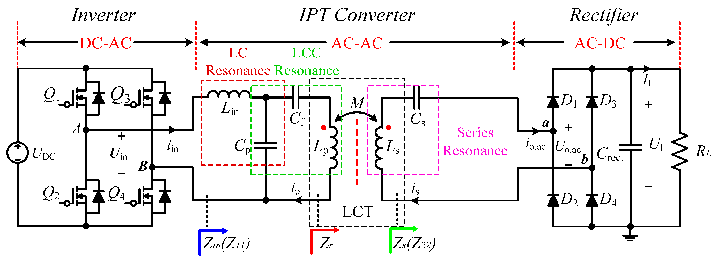
3.2. Selecting Compensation Topology

After determining the wireless pad design, a compensation topology design suitable for the input/output characteristics was conducted. The compensation topologies mainly used in IPT systems include Series-Series (S-S), LCC-S, and DS-LCC topologies with high-dimensional topologies that resonate in series with both the transmitter and receiver pads. Table 3 provides brief descriptions of the characteristics of S-S, LCC-S, and DS-LCC.
The S-S compensation topology requires two additional capacitors (for resonance), one transmitter, and one receiver. The S-S topology has the advantages of a small number of resonance elements and a constant current (CC) output characteristic. However, the S-S topology has an overvoltage application problem due to increased output characteristics when k decreases due to separation distance fluctuations. In addition, it is sensitive to pad inductance fluctuations, meaning there is a risk of switch faults.
The LCC-S compensation topology is a high-order topology in which resonance inductors (Lin) and resonance capacitors (Cp, Cf, Cs) are added to solve the bifurcation problem caused by load and separation distances in the basic compensation topology configuration. Furthermore, this higher-order topology achieves higher AC equivalent circuit accuracy because there are more resonant filter elements compared to the basic compensation topology. Since the LCC-S has a constant voltage (CV) characteristic, this provides the advantage of not exacerbating an open circuit accident.
The DS-LCC is designed with a high-dimensional compensation topology for both the transmitter and receiver and has CC characteristics. The DS-LCC topology also has the advantage that the bifurcation problem due to separation distance can be solved and the output characteristics can be designed flexibly by the manufacturer. However, the DS-LCC has many resonant elements (two resonant inductors and four resonant capacitors), which is disadvantageous in terms of cost and volume. MVDC class voltage/current sensors should supply stable power, even when the separation distance fluctuates. The S-S compensation topology has the problem that the output current increases when the mutual inductance decreases as the separation distance occurs [26]. Therefore, using a high-dimensional compensation topology is suitable. Considering the volume limit inside the receiver, the LCC-S topology with CV characteristics was selected. The IPT converter configured with the LCC-S topology is displayed in Figure 8.
After selecting the compensation topology, the maximum allowable current flowing through the wireless pad should be considered. Since the output characteristics vary according to the separation distance, the coil should operate stably under maximum current stress conditions. A graph of the output voltage and input phase according to separation distance is presented in Figure 9. This graph demonstrates that zero voltage switching was maintained, even when the position of the wireless pad was changed. The maximum current of the voltage/current sensor to be supplied was less than 4 A. Since the average allowable current of the employed litz wire was 2.5 [A/mm2], a 1 mm diameter litz wire consisting of 0.10mm 150 strands was used for the receiving pad. The impedance condition at the resonant frequency (fr) when operating the LCC-S topology is as follows:
Z s = j ω r L s + 1 j ω r C s + R o , a c R o , a c ,
j ω r L i n + 1 j ω r C p = 0 ,   j ω r L p + 1 j ω r C p + 1 j ω r C f = 0 .
The reflected impedance, which is converted from the secondary side to the primary side, is deduced as
Z r = ( ω M ) 2 Z s .
The total input impedance of the LCC-S topology can be derived as follows:
Z i n = j ω L i n + 1 j ω C p + 1 j ω L p   +   1 j ω C f   +   Z r .
Based on Kirchhoff’s current law, the current flowing through the transmitter and receiver pads and the output voltage of the LCC-S are as follows [23]:
i p = U i n j ω L i n ,
i s = j ω M I p R o , a c = M U i n L i n R o , a c ,
U o , a c M U i n L i n
Equation (11) demonstrates that the current flowing through the transmitter pad is affected by the operating frequency (fo), Uin, and Lin. Moreover, a constant current flows regardless of any changes in separation distance. Equation (13) indicates that the output voltage is determined by the M value of the pad, the DC input voltage, and Lin. Therefore, to meet the output voltage characteristic requirements of the MVDC sensor, the transmitter pad, receiver pad, and resonant inductor should be designed, and the resonance frequency and coil diameter should be selected, by considering the coil losses due to the wireless pad. The specifications of the wireless pad and the selection of the resonant network values are presented in Section 4.

4. Verification of Inductive Power Transfer System through Simulations and Experimental Prototype

In this section, based on the analysis in Section 3, the wireless pad prototype is designed, and the wireless pad characteristics are analyzed to select the operating frequency and resonance network element values. After the IPT system is built, the variable output characteristics are verified through experiments.

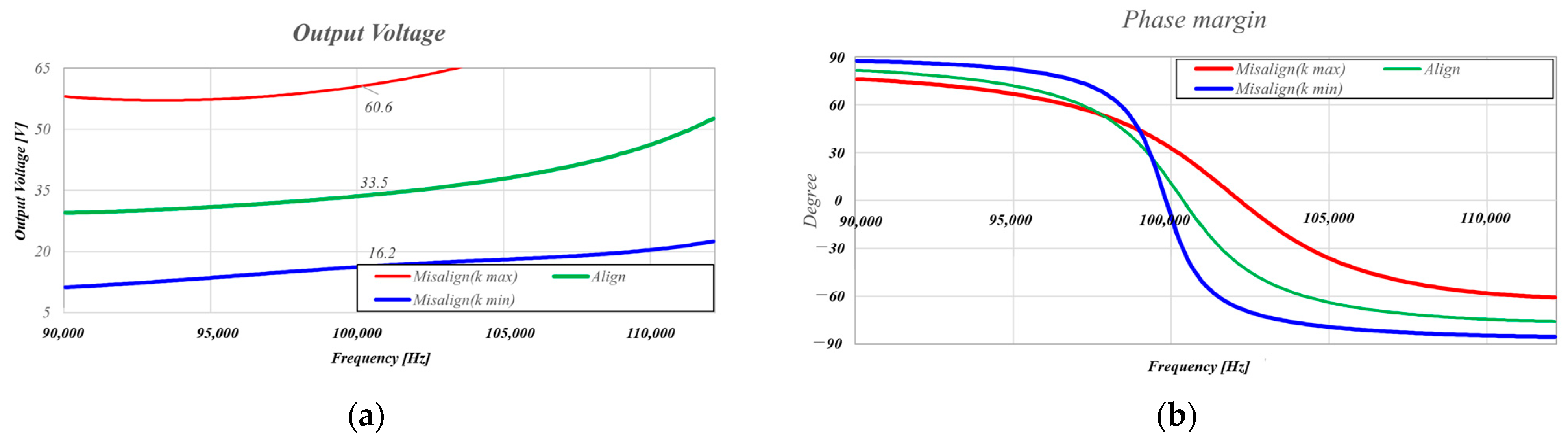
4.1. Selecting Parameter and Frequency

Based on the 3D FEM simulation results, prototype wireless pads were designed and manufactured. Figure 10 displays the fabricated transmitter and receiver pads, which were manufactured by considering the output voltage, current stress, and operating frequency. The transmitter coil consisted of 15 turns on the 1st layer and 5 turns on the outer diameter side of the 2 layers, totaling 20 turns. The receiver coil consisted of 13 turns on one layer. The k range was calculated by measuring the self-inductance and leakage inductance with an LCR meter. As the number of turns of the wireless pad increased, M increased. However, the diameter of the wireless pad coil had to be reduced due to the increase in volume caused by the increase in the number of wireless pad coil winding turns. Based on Equations (7)–(13), the design of an appropriate value range between the pad inductance and Lin was selected. The load voltage range was designed to be 15–50 V, which was the voltage range required by the regulator. Considering the output voltage range, Lin was designed as 34.36 [uH]. After manufacturing the wireless pad and Lin, the operating frequency range to build an IPT system was selected. Because of the limited performance of the MOSFETs in the laboratory, the maximum operating frequency was selected as 100 kHz. Substituting this value into Equation (13), the transmitter pad current was confirmed as approximately 5.2 A, as displayed in Figure 11.
Based on fo, Lin, Cp, Cf, and Cs were selected based on Equations (8) and (9). For the resonance capacitor, a multi-layer ceramic capacitor (MLCC) was employed, as these have robust high-frequency characteristics. Figure 12 presents the experimental prototype for verifying IPT system operation. The input voltage was fixed at 110 V, and the range of k was 0.06–0.20 because the wireless pad design was required to derive an appropriate pad inductance value. Table 4 shows the prototype IPT converter prototype measured parameters.

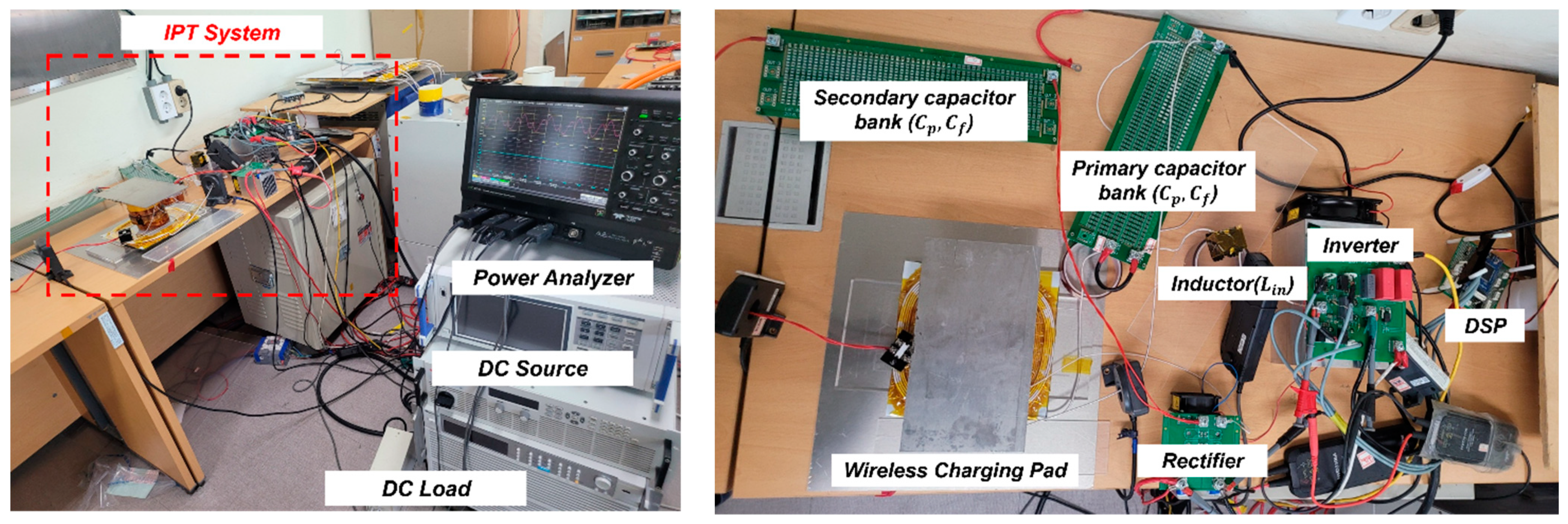
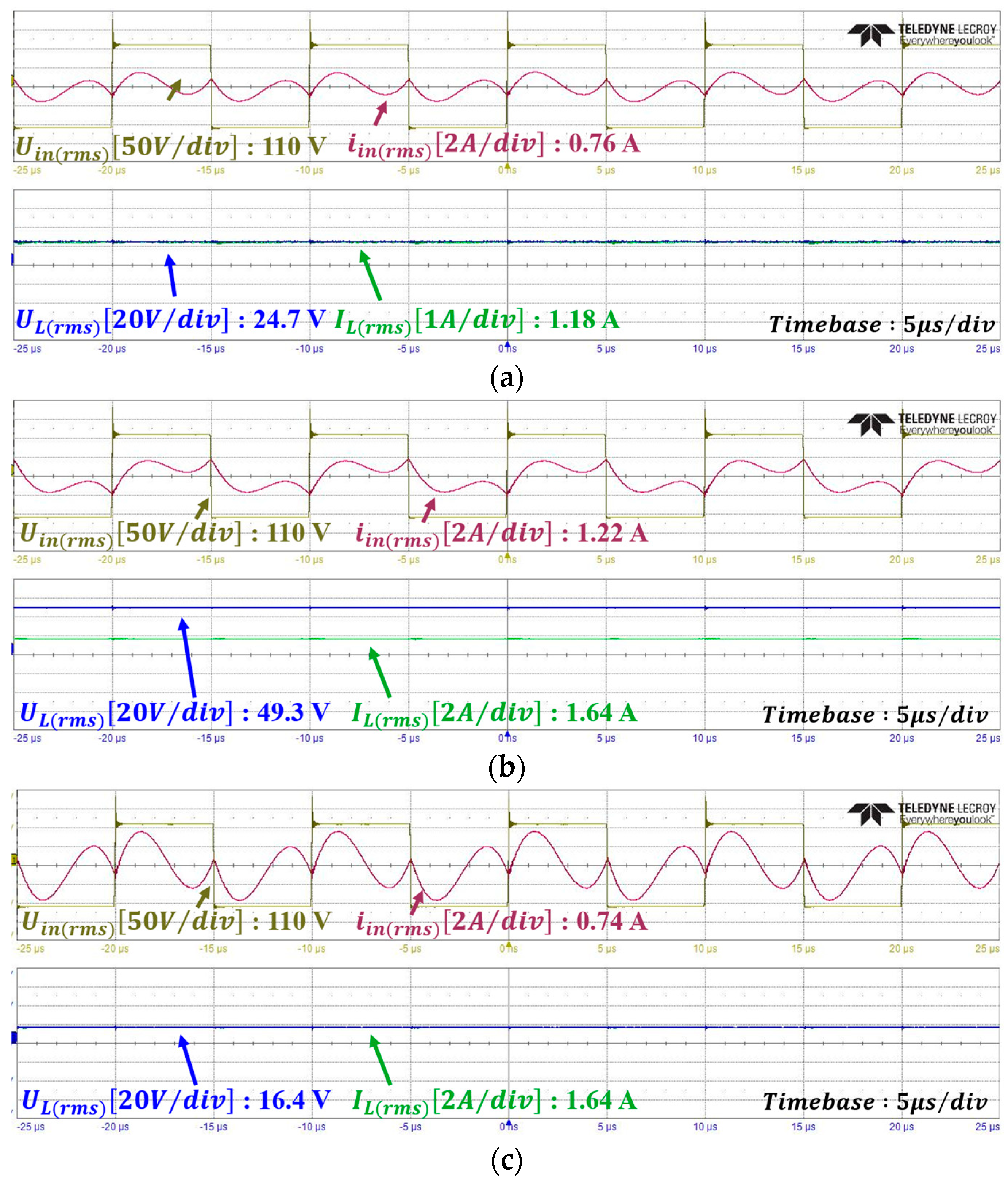
4.2. Experimental Results

Figure 13 presents the experimental results for the aligned, maximum k (z = 30 mm) misaligned, and minimum k (z = 90mm) misaligned conditions using a HIOKI PW6001 power analyzer. The experimental results confirmed that the output voltage was in the range of 16.3–49.3 V, which was achieved within the input voltage range of the voltage regulator. The difference in the output voltage range was caused by the voltage drop due to the parasitic resistance component of the resonance device and the reactance error of the passive device. However, this difference was considered negligible. The output current varied according to the value of the load resistance. Figure 14 displays the input and output waveforms in the aligned, misaligned in maximum k (z = 30mm), and misaligned in minimum k (z = 90mm) states, respectively. Figure 14 confirmed that ZVS operation was achieved with a square wave output.

5. Conclusions

In this paper, a power supply system for MVDC-grade voltage/current measuring instruments using a magnetic induction method was proposed and verified. The receiving pad was constructed by considering the size of the MVDC-grade voltage/current measuring instrument, and the separation distance range was selected according to the air insulation voltage value required between the transmitting and receiving pads. A coil design was selected that minimized any variations in the k value according to the range of separation distance fluctuations. Moreover, the operating frequency and magnetic inductance (turn count and layer count) were selected to accommodate the maximum current flowing in the coil. A high-dimensional resonance network was considered for the transmitter to prevent bifurcation problems caused by separation distance fluctuations during IPT system operation, and an LCC-S topology was selected. For the output voltage range, the proposed IPT power supply system had output characteristics of 16 V at the maximum separation distance and 50 V at the minimum separation distance, and ZVS operation was achieved. The coil winding design, magnetic inductance, and k value were selected using 3D FEM simulations, and their validity was verified through operation after the IPT system was designed similarly to that used in a laboratory environment. The experimental results confirmed that the IPT system can satisfy the power characteristics required by the MVDC current sensor from the minimum insulation distance of 30 mm to the maximum vertical misalignment of 90 mm with ZVS operation. Therefore, the IPT system could be selected as a power supply method for the MVDC voltage/current measuring instrument considering its insulation safety and ability to meet the range of output characteristics due to the separation of distance fluctuations.

Author Contributions

Conceptualization, S.J., J.-H.A. and D.-H.K.; methodology, S.J. and G.L.; validation, S.J.; formal analysis, G.L.; investigation, S.J.; writing—original draft preparation, S.J.; writing—review and editing, J.-H.A. and D.-H.K. All authors have read and agreed to the published version of the manuscript.

Funding

This work was supported by the Korea Institute of Energy Technology Evaluation and Planning (KETEP) grant funded by the Korean government (MOTIE) (20225500000120).

Conflicts of Interest

The authors declare no conflict of interest.

References

  1. Dragičević, T.; Lu, X.; Vasquez, J.C.; Guerrero, J.M. DC Microgrids—Part II: A Review of Power Architectures, Applications, and Standardization Issues. IEEE Trans. Power Electron. 2016, 31, 3528–3549. [Google Scholar] [CrossRef]
  2. Doncker, R. Power electronic technologies for flexible DC distribution grids. In Proceedings of the 2014 International Power Electronics Conference (IPEC-Hiroshima 2014—ECCE ASIA), Hiroshima, Japan, 18–21 May 2014; pp. 736–743. [Google Scholar]
  3. Coffey, S.; Timmers, V.; Li, R.; Wu, G.; Egea-Àlvarez, A. Review of MVDC Applications, Technologies, and Future Prospects. Energies 2021, 14, 8294. [Google Scholar] [CrossRef]
  4. Stieneker, M.; Doncker, R.D. Medium-voltage DC distribution grids in urban areas. In Proceedings of the 2016 IEEE 7th International Symposium on Power Electronics for Distributed Generation Systems (PEDG), Vancouver, BC, Canada, 27–30 June 2016; pp. 1–7. [Google Scholar]
  5. Zhang, L.; Sun, K.; Xing, Y.; Feng, L.; Ge, H. A modular grid-connected photovoltaic generation system based on dc bus. IEEE Trans. Power Electron. 2011, 26, 523–531. [Google Scholar] [CrossRef]
  6. Langenberg, N.; Kimpeler, S.; Moser, A. Interconnecting Power-Electronic Buck Converter Modules in a Novel High-Power Test Bench for MVDC Circuit Breakers. Energies 2022, 15, 7915. [Google Scholar] [CrossRef]
  7. Chiumeo, R.; Raggini, D.; Veroni, A.; Clerici, A. Comparative Analysis of PI and ADRC Control through CHIL Real Time Simulations of a DC-DC DAB into a Multi-Terminal MVDC/LVDC Distribution Network. Energies 2022, 15, 7631. [Google Scholar] [CrossRef]
  8. Qi, L.; Antoniazzi, A.; Raciti, L. DC distribution fault analysis, protection solutions, and example implementations. IEEE Trans. Ind. Appl. 2018, 54, 3179–3186. [Google Scholar] [CrossRef]
  9. Huang, X.; Qi, L.; Pan, J. A new protection scheme for MMC-based MVdc distribution systems with complete converter fault current handling capability. IEEE Trans. Ind. Appl. 2019, 55, 4515–4523. [Google Scholar] [CrossRef]
  10. Li, G.; Zhang, L.; Joseph, T.; Liang, J.; Yan, G. Comparisons of MVAC and MVDC Systems in Dynamic Operation, Fault Protection and Post-Fault Restoration. In Proceedings of the 2019—45th Annual Conference of the IEEE Industrial Electronics Society, Lisbon, Portugal, 14–17 October 2019. [Google Scholar]
  11. Simiyu, P.; Xin, A.; Wang, K.; Adwek, G.; Salman, S. Multiterminal Medium Voltage DC Distribution Network Hierarchical Control. Electronics 2020, 9, 506. [Google Scholar] [CrossRef]
  12. Wang, B.; Dehghanian, P.; Wang, S.; Mitolo, M. Electrical safety considerations in large-scale electric vehicle charging 453 stations. IEEE Trans. Ind. Appl. 2019, 55, 6603–6612. [Google Scholar] [CrossRef]
  13. Freschi, F.; Mitolo, M.; Tommasini, R. Electrical safety of plug-in electric vehicles: Shielding the public from shock. IEEE Ind. Appl. Mag. 2018, 24, 58–63. [Google Scholar] [CrossRef]
  14. Mayordomo, I.; Drager, T.; Spies, P.; Bernhard, J.; Pflaum, A. An overview of technical challenges and advances of inductive wireless power transmission. Proc. IEEE 2013, 101, 1302–1311. [Google Scholar] [CrossRef]
  15. Sohn, Y.H.; Choi, B.H.; Lee, E.S.; Lim, G.C.; Cho, G.H.; Rim, C.T. General unified analyses of two-capacitor inductive power transfer systems: Equivalence of current-source SS and SP compensations. IEEE Trans. Power Electron. 2015, 30, 6030–6045. [Google Scholar] [CrossRef]
  16. Zhang, Z.; Pang, H.; Georgiadis, A.; Cecati, C. Wireless Power Transfer—An Overview. IEEE Trans. Ind. Electron. 2019, 66, 1044–1058. [Google Scholar] [CrossRef]
  17. Dong, Y.; Dong, S.-W.; Wang, Y.; Gong, L. Calibration method of retrodirective antenna array for microwave power transmission. In Proceedings of the 2013 IEEE Wireless Power Transfer (WPT), Perugia, Italy, 15–16 May 2013; pp. 41–43. [Google Scholar]
  18. Jin, K.; Zhou, W. Wireless Laser Power Transmission: A Review of Recent Progress. IEEE Trans. Power Electron. 2019, 34, 3842–3859. [Google Scholar] [CrossRef]
  19. Zhang, H.; Jin, K.; Zhou, W. Simultaneous Wireless Power and Data Transmission for Laser Power Transfer System Based on Frequency-Shift Keying Modulation Method. In Proceedings of the 2022 IEEE Applied Power Electronics Conference and Exposition (APEC), Houston, TX, USA, 20–24 March 2022; pp. 1874–1877. [Google Scholar]
  20. Sheng, Q.; Geng, J.; Chang, Z.; Wang, A.; Wang, M.; Fu, S.; Yao, J. Adaptive Wireless Power Transfer via Resonant Laser Beam Over Large Dynamic Range. IEEE Internet Things 2023, 10, 8865–8877. [Google Scholar] [CrossRef]
  21. He, T.; Zheng, G.; Wu, Q.; Huang, H.; Wan, L.; Xu, K.; Shi, T.; Lv, Z. Analysis and Experiment of Laser Energy Distribution of Laser Wireless Power Transmission Based on a Powersphere Receiver. Photonics 2023, 10, 844. [Google Scholar] [CrossRef]
  22. Liu, C.; Hu, A.P.; Nair, N.C. Modelling and analysis of a capacitively coupled contactless power transfer system. IET Power Electron. 2011, 4, 808–815. [Google Scholar] [CrossRef]
  23. Mishra, S.K.; Adda, R.; Sekhar, S.; Joshi, A.; Rathore, A.K. Power transfer using portable surfaces in capacitively coupled power transfer technology. IET Power Electron. 2016, 9, 997–1008. [Google Scholar] [CrossRef]
  24. Mahdi, H.; Hattori, R.; Hoff, B.; Uezu, A.; Akiyoshi, K. Design Considerations of Capacitive Power Transfer Systems. IEEE Access 2023, 11, 57806–57818. [Google Scholar] [CrossRef]
  25. IEEE Std 1427-2020 (Revision of IEEE Std 1427-2006); IEEE Guide for Recommended Electrical Clearances and Insulation Levels in Air Insulated Electrical Power Substations. IEEE: Piscataway, NJ, USA, 2021; pp. 1–51.
  26. Li, W.; Zhao, H.; Deng, J.; Li, S.; Mi, C.C. Comparison Study on SS and Double-Sided LCC Compensation Topologies for EV/PHEV Wireless Chargers. IEEE Trans. Veh. Technol. 2016, 65, 4429–4439. [Google Scholar] [CrossRef]
Figure 1. Medium voltage direct current (MVDC) grid.
Electronics 12 04702 g001
Figure 2. MVDC class voltage/current sensor basic specification.
Electronics 12 04702 g002
Figure 3. Inductive power transfer (IPT) system.
Electronics 12 04702 g003
Figure 4. AC equivalent circuit of IPT system based on network circuit method.
Electronics 12 04702 g004
Figure 5. (a) Magnetic flux path of a circular pad (CP), and (b) magnetic flux path of the double-D pad (DDP).
Electronics 12 04702 g005
Figure 6. FEM Simulation designs: (a) circular pad (b) double-D pad.
Electronics 12 04702 g006
Figure 7. Coupling coefficient graph according to vertical distance: (a) with x, y = 0 mm; (b) with x = 20 mm, y = 10 mm.
Electronics 12 04702 g007
Figure 8. LCC-S compensation topology.
Electronics 12 04702 g008
Figure 9. LCC-S compensation topology: (a) output voltage, and (b) input phase margin.
Electronics 12 04702 g009
Figure 10. Wireless pad: (a) transmitter pad and (b) receiver pad.
Electronics 12 04702 g010
Figure 11. Transmitter pad current graph according to operating frequency.
Electronics 12 04702 g011
Figure 12. Experimental prototype.
Electronics 12 04702 g012
Figure 13. Experimental measurement results with HIOKI PW6001: (a) aligned state; (b) misaligned (z = 30 mm) state; and (c) misaligned (z = 90 mm) state.
Electronics 12 04702 g013
Figure 14. Experimental waveforms: (a) aligned state; (b) misaligned (z = 30 mm) state; and (c) misaligned (z = 90 mm) state.
Electronics 12 04702 g014
Table 1. Wireless power transfer (WPT) classification and characteristics.
MethodIPTMPTLPTCPT
FigureElectronics 12 04702 i001Electronics 12 04702 i002Electronics 12 04702 i003Electronics 12 04702 i004
Transmission powerUp to several hundred kWUp to several kWUp to several WUp to several kW
Frequency rangeUp to several hundred kHzSeveral GHz-Several MHz
MeritsHigh efficiency,
mature technology,
safe for humans
Very long distances
(several km)
Long distance (several km)Light weight of the pad
DemeritsShort distance,
output fluctuations by distance
Harmful for humans,
low efficiency (10–50%),
large antennas
Low efficiency (up to 20%), low powerNo commercialization,
need for high-spec power semiconductors
Table 2. IPT system design requirements.
SymbolsParametersValues [Unit]
UDCDC input voltage110 [V]
110 [V]Vertical distance range30–90 [mm]
xx-axis distance range0–20 [mm]
yy-axis distance range0–10 [mm]
ULIPT output voltage range 15–50 [V]
Po,maxMaximum output power50 [W]
Table 3. IPT system design requirements.
TopologyS-SLCC-SDS-LCC
FigureElectronics 12 04702 i005Electronics 12 04702 i006Electronics 12 04702 i007
Output characteristicCCCVCC
Number of resonance
components
246
Output power at
misalignment
IncreaseDecreaseDecrease
Coil design flexibilityBadNormalGood
Does bifurcation occurOXX
Table 4. IPT converter prototype measured parameters.
SymbolsParametersValues [Unit]
LpTransmitter pad inductance149.79 [uH]
LsReceiver pad inductance39.88 [uH]
kCoupling coefficient0.06–0.20
LinResonance inductor34.36 [uH]
CpParallel resonance capacitor74.81 [nF]
CfSeries resonance capacitor21.70 [nF]
CsReceiver resonance capacitor64.22 [nF]
foOperating frequency100 [kHz]
Disclaimer/Publisher’s Note: The statements, opinions and data contained in all publications are solely those of the individual author(s) and contributor(s) and not of MDPI and/or the editor(s). MDPI and/or the editor(s) disclaim responsibility for any injury to people or property resulting from any ideas, methods, instructions or products referred to in the content.

