Article

A 62 ppm MDR Deviation and Sub-250 ns MTIE Railway Balise

1
Research and Development Center of Healthcare Electronics, Institute of Microelectronics of the Chinese Academy of Sciences, Beijing 100029, China
2
School of Integrated Circuits, University of Chinese Academy of Sciences, No. 19(A) Yuquan Road, Shijingshan District, Beijing 100049, China
3
Beijing Key Laboratory of RFIC Technology for Next Generation Communications, Institute of Microelectronics of the Chinese Academy of Sciences, Beijing 100029, China
4
CRSC Research and Design Institute Group Co., Ltd., Beijing 100070, China
*
Authors to whom correspondence should be addressed.
Electronics 2023, 12(20), 4217; https://doi.org/10.3390/electronics12204217
Submission received: 6 September 2023 / Revised: 2 October 2023 / Accepted: 10 October 2023 / Published: 11 October 2023
(This article belongs to the Topic Electric Vehicles Energy Management)

Abstract

:
A balise is a specialized device utilized for train communication and control. However, existing balises are composed of separate components, resulting in high production costs, low integration, and significant room for improvement in stability. We propose an integrated solution, to enhance the integration of balises, reducing the number of discrete components. Additionally, we propose a feedback-enabled energy extraction circuit with a limiter-based startup circuit, to enhance the stability of the balise system. The prototype was fabricated using 180 nm high voltage(HV) complementary metal oxide semiconductor(CMOS) technology. Once implemented in the balise, the number of discrete components in the system is reduced by 25%, and the system can start up within 20 ms and operate stably. The mean data rate (MDR) deviation of the balise is only 62 ppm, which is 69% lower than that specified in the test specification for the Eurobalise form–fit–function interface specification (FFFIS), and the maximum time interval error (MTIE) is less than 250 ns.

1. Introduction

The BTS (balise transmission system) is widely used in the CTCS (Chinese train control system) and the CBTC (communication-based train control system), as shown in Figure 1a [1,2,3,4,5,6]. The system is composed of a BTM (balise transmission module), an antenna, an LEU (lineside electronic unit), a balise, cable, and the TCC (train control center). Figure 1b shows the structure block diagram of the BTS system. The BTM and antenna are onboard equipment. The balise (including an active balise and a passive balise), LEU, and TCC are ground equipment. The TCC will transmit a differential superposition signal to the balise through the LEU and the cable. The interface between the active balise and the LEU is called ‘C’. When the train passes, the passive balise is activated and then communicates with the BTM through the antenna.
As shown in Figure 2, the balise mainly consists of an interface circuit, an active balise, including an energy extraction circuit and a clock data recovery circuit, and a passive balise. The interface circuit separates the C signal sent by the LEU into C6 and C1 signals, and then the energy extraction circuit converts the C6 signal into a stable power supply, to power the clock data recovery circuit, which extracts the clock and the data signal in the C1 signal and gives it to the passive balise. When a train passes by, the BTM releases a signal through an antenna, to activate the passive balise and exchange information.
Many studies have focused on the onboard hardware BTM [7,8,9], but there has been very little research on ground systems, especially balises. Current railway balises are typically constructed at the board level and entail the extensive utilization of discrete components, which leads to relatively low stability. This paper presents an integrated active balise, and the prototype was implemented in 180 nm HV CMOS technology. After being applied to the balise system, the number of discrete components was reduced by 25%. The mean data rate (MDR) deviation of the balise was only 62 ppm, which was 69% lower than that specified in the test specification for the Eurobalise form–fit–function interface specification (FFFIS) [10,11], and the maximum time interval error (MTIE) [12,13,14] was less than 250 ns (1000-bit test).
The rest of this paper is organized as follows. Section 2 presents the materials and methods of this paper, including the design of the energy extraction circuit and the clock data recovery circuit. Section 3 shows the results of this work, primarily focusing on the test results of the circuits. Section 4 shows the discussion. Conclusions are given in Section 5.

2. Materials and Methods

In this section, we will introduce the integration solution for the active balise shown in Figure 2, which includes the design of the energy extraction circuit and the clock data recovery circuit. The energy extraction circuit, in particular, consists of the substrate-adaptive rectifier and the BGR–LDO feedback regulator.

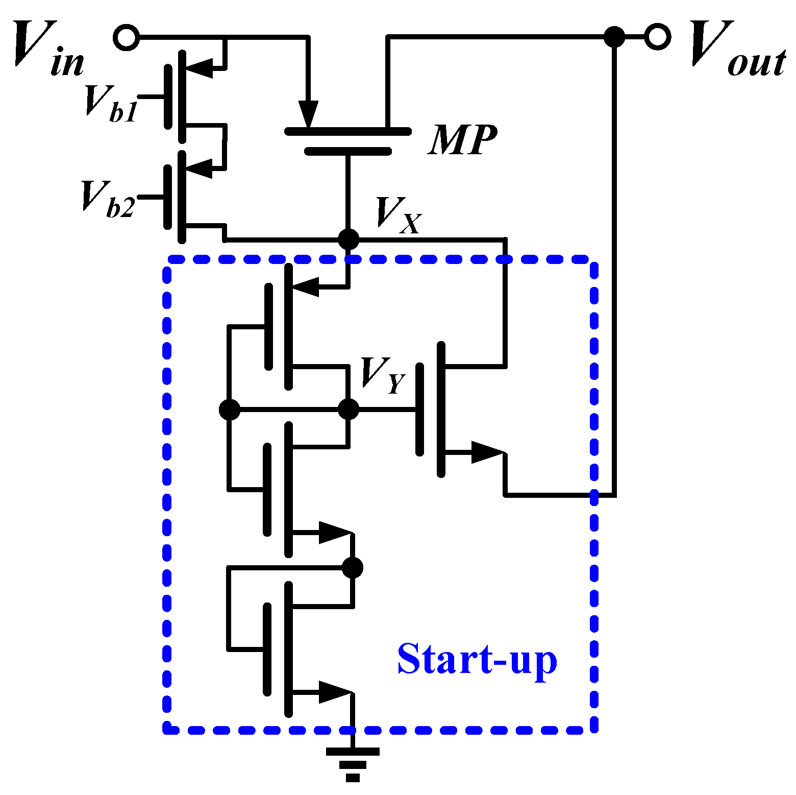
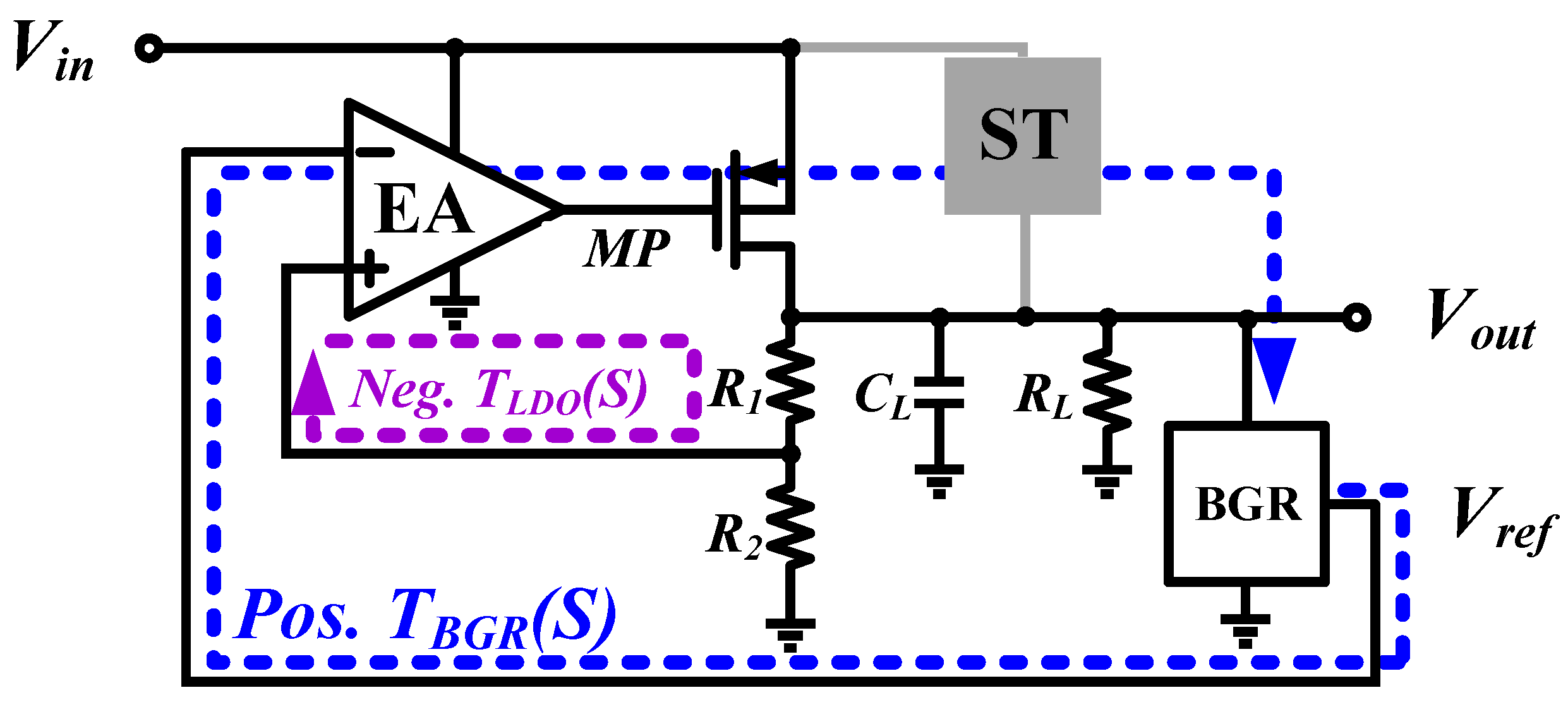
2.1. Design of the Energy Extraction Circuit

The energy extraction circuit is responsible for converting the C6 signal, which is separated from the interface circuit, into a stable DC power supply. The diagram is depicted in Figure 3. Initially, the rectifier completes the AC–DC conversion of the C6 signal, followed by the use of a low dropout regulator (LDO) and a bandgap reference (BGR) circuit, to further stabilize the output.
The limiter and start-up circuit are designed to increase the reliability of the circuit. Due to the varying lengths of LEU cables, the range of the C6 signal experiences significant fluctuations. Consequently, after passing through the rectifier, the voltage range becomes relatively large. To ensure that instantaneous high voltages do not damage the subsequent stages of the circuit, and to enhance circuit reliability, the addition of a limiter is necessary. Similarly, during power-up, the circuit may not start immediately. Therefore, it is essential to add a system-level start-up circuit, to ensure the proper initialization of the circuit. This aspect will be explained in detail in Section 2.1.2.

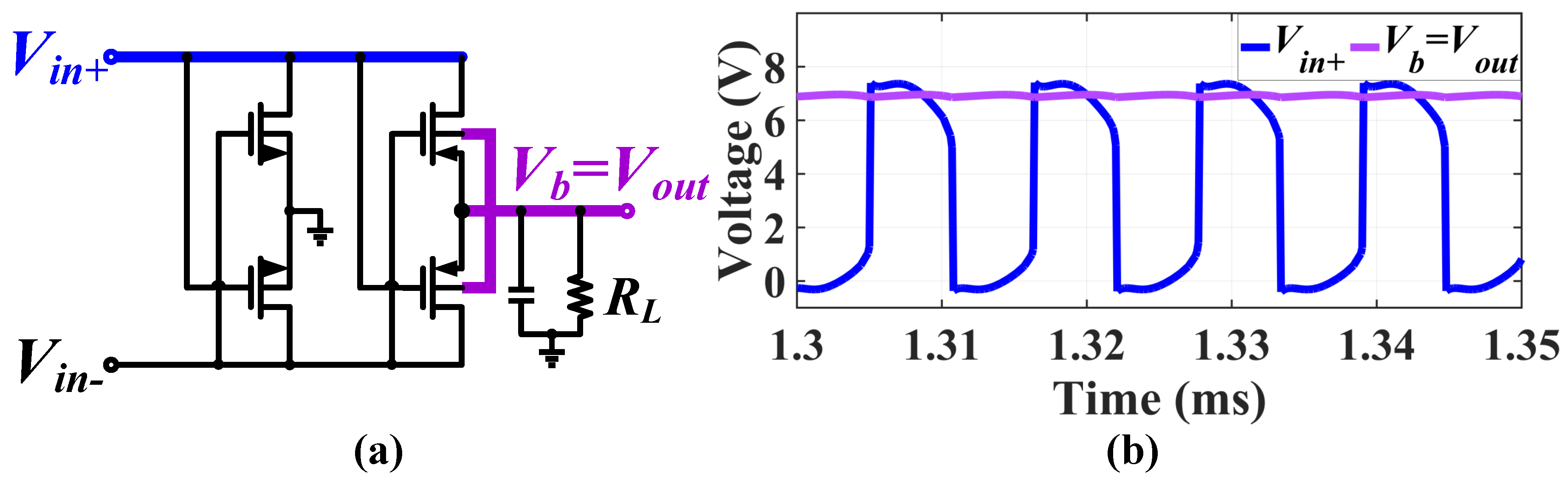
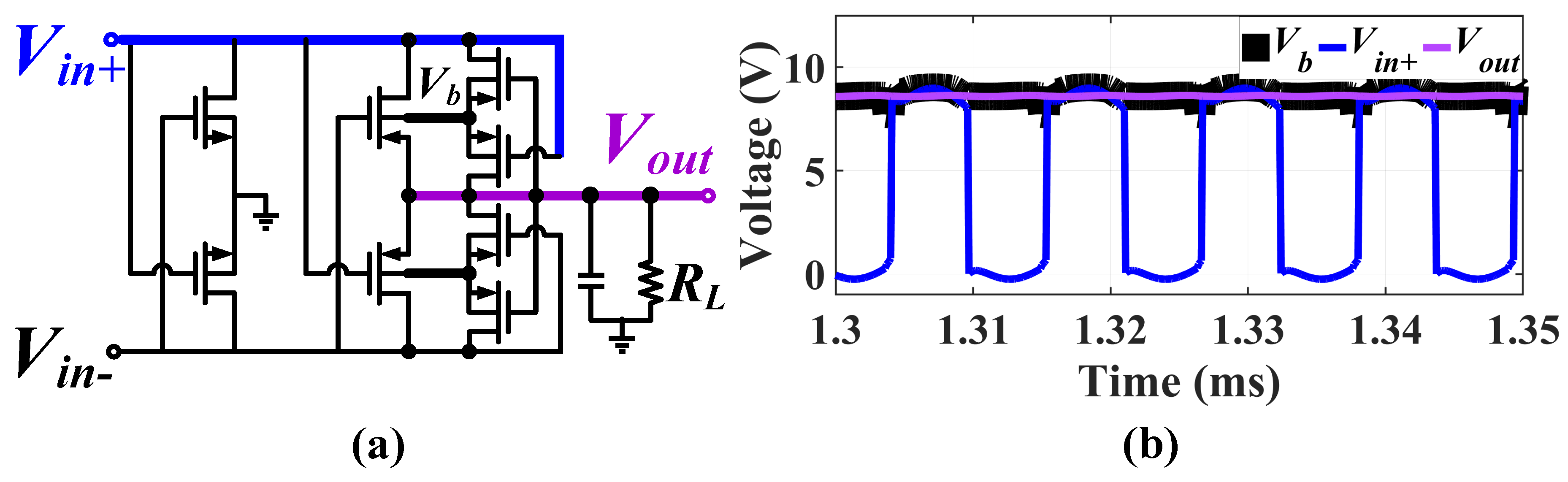
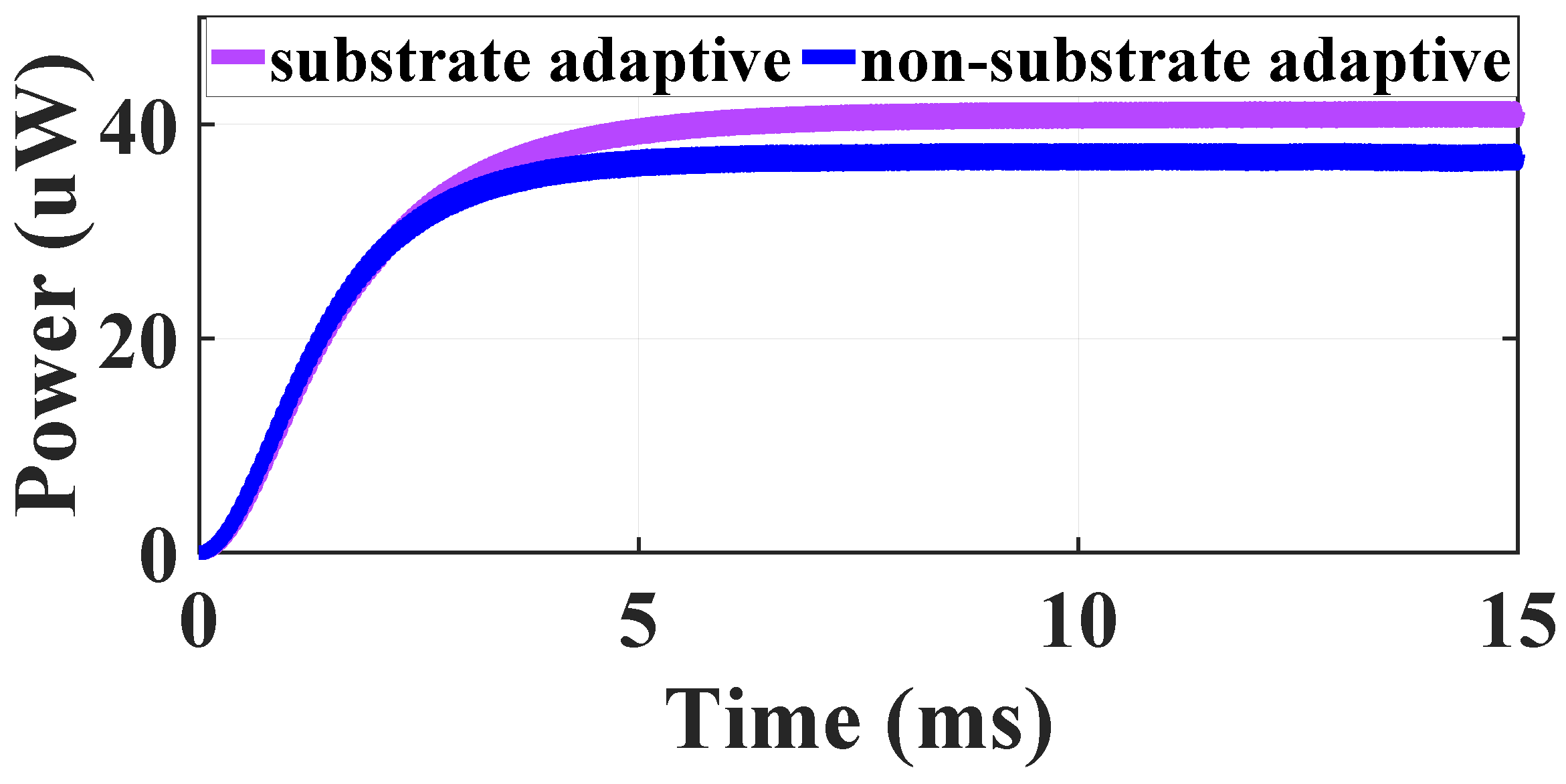
2.1.1. Substrate-Adaptive Rectifier

Due to the relatively high internal resistance of the LEU itself, coupled with the resistance introduced by the long cable lines, the input impedance of the circuit must be very high, to achieve a higher input voltage for improving the output voltage. However, increasing the input impedance of the rectifier would require reducing the width-to-length ratio of the transistors, which, in turn, would decrease the output current. Therefore, there exists a trade-off between increasing the output voltage and increasing the output current. Enhancing the output power of the rectifier has always been a crucial aspect of power management systems.
In Figure 4a, the NMOS and PMOS gate cross rectifier eliminates the threshold voltage drop [15,16,17]. However, because the substrate voltage V b of the PMOS is always connected to the output voltage V o u t , sometimes it is lower than the input voltage V i n + , as shown in Figure 4b. This causes the substrate voltage of the PMOS to not always be at the highest voltage, resulting in substrate leakage current and a decrease in input impedance. This, in turn, causes the input voltage to be pulled down and reduces the output voltage and output power.
To enhance the output power, ref. [18] proposed a rectifier that reduced the losses caused by threshold voltage drops and increased the output voltage, using bootstrap voltage techniques. However, this circuit introduced capacitors and switches, which increased circuit complexity. In [19], the output power of the rectifier bridge was increased, by increasing the order of the energy harvesting circuit. However, this introduced inductors, which increased the circuit’s footprint.
We employed a substrate adaptive rectifier, as illustrated in Figure 5a. We designed a substrate adaptive circuit for the PMOS that allowed its substrate voltage V b to be chosen between V o u t and V i n . This ensured that the substrate voltage was always at the highest voltage, as shown in Figure 5b, thereby reducing the substrate leakage current of the PMOS, maintaining stable impedance matching, and improving the output power of the rectifier.
Under a load consisting of a 1 K Ω resistor and a 10 μ F capacitor, we conducted simulations, to measure the output voltage and current of the rectifier and to determine its output power:
P o u t = V o u t × I R L .
As shown in Figure 6, the simulation results of the rectifier’s output power demonstrated a 10.8% increase after the addition of the substrate adaptive circuit.

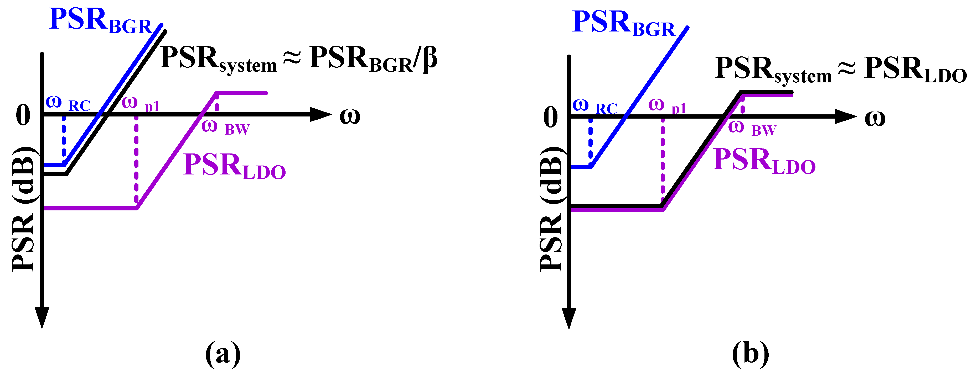
2.1.2. BGR–LDO Feedback Regulator

The role of the regulator is to further stabilize the voltage after it has been processed by the rectifier. It is the most critical component in the energy extraction circuit. Voltage regulators typically consist of a bandgap reference circuit and a low-dropout linear regulator. The bandgap reference circuit generates a temperature-independent and highly stable reference voltage, which is then supplied to the low-dropout linear regulator. Subsequently, the low-dropout linear regulator, through a negative feedback loop, outputs a stable DC voltage, providing power to the system.
Figure 7 illustrates a conventional regulator, in which V i n provides power to both the BGR and the error amplifier (EA), followed by the BGR supplying a reference voltage to the LDO [20,21,22]. When a ripple Δ V i n occurs on V i n , it will propagate through two paths to V o u t . The first path is through the LDO comprising the EA and MP, while the second path is through the BGR, before being input into the LDO, to reach V o u t . Therefore, Δ V o u t is
Δ V o u t = Δ V i n × P S R L D O + Δ V i n × P S R B G R × 1 β = Δ V i n × ( P S R L D O + P S R B G R × 1 β ) ,
where
P S R L D O = Δ V o u t Δ V i n , P S R B G R = Δ V B G R Δ V i n , β = R 2 R 1 + R 2 .
By using Equations (2) and (3), we can obtain
P S R s y s t e m | c o n v e n t i o n a l = Δ V o u t Δ V i n = P S R L D O + P S R B G R × 1 β .
One way to improve the PSR of the system is to enhance the PSR of the LDO and the BGR. When it comes to the LDO, at low frequencies,
P S R L D O = 1 1 + A E A × β .
The A E A is the DC gain of the EA [23,24]. As the frequency rises to the main pole, the loop gain begins to decrease, and the PSR of the LDO begins to decrease. Until the frequency reaches the unit gain bandwidth, the PSR of the LDO is determined by the gain of MP:
P S R L D O = g m p × ( r D S / / R L ) .
Where g m p is the transconductance of MP, r D S is the drain-source resistance of MP, and R L is the load resistance of the circuit [25,26]. To enhance the PSR of the LDO at high frequencies, it is necessary to increase the unity gain bandwidth of the EA, as discussed in [27,28]. However, the bandwidth of the amplifier is directly proportional to transconductance:
B W = g m × C .
Increasing the bandwidth by raising the transconductance leads to higher power consumption. Regarding the BGR, the amplifier in the circuit largely determines the PSR and, due to its inherent characteristics, the PSR tends to decrease at high frequencies. Improving the PSR of the BGR can be achieved by enhancing the amplifier, but this would significantly increase the circuit complexity and power consumption, as discussed in [29,30].
Figure 8 depicts the designed BGR–LDO feedback regulator. In this structure, the input voltage V i n only supplies power to the EA and MP, while the BGR is powered by the output of the LDO and then generates reference voltage for the LDO.
For the proposed regulator, once the circuit is operational, if the start-up circuit (ST) is turned off, there are two main paths from V i n to V o u t . The first path is from V i n through the EA and MP to V o u t , while the second path is from V o u t through the BGR, then through the LDO for voltage regulation, before reaching V o u t . As the power supply to the BGR is the voltage stabilized by the LDO, the output voltage of the BGR is more stable compared to the conventional structure. Consequently, the system’s output voltage is also more stable. When a ripple Δ V i n is present on V i n , the resulting output ripple Δ V o u t is
Δ V o u t = Δ V i n × P S R L D O + Δ V o u t × P S R B G R × 1 β = Δ V i n × P S R L D O 1 P S R B G R × 1 β .
Thus, the PSR of the proposed regulator is
P S R s y s t e m | p r o p o s e d = Δ V o u t Δ V i n = P S R L D O 1 P S R B G R × 1 β .
When the performance of the BGR is poor (that is, when the P S R B G R is poor, e.g., −30 dB, ≪ β ), then
P S R s y s t e m | c o n v e n t i o n a l P S R B G R × 1 β ,
P S R s y s t e m | p r o p o s e d P S R L D O .
Figure 9 shows the power supply rejection (PSR) of two structures. The PSR of the conventional structure is more affected by the BGR, while the PSR of the proposed structure is more related to the LDO. In other words, for the same LDO, the proposed structure can effectively alleviate the impact of the BGR on the PSR, reducing the design complexity and power consumption of the BGR. We carried out alternating current(AC) analysis on the two structures, to prove the feasibility of the proposed structure, as shown in Figure 10. The simulation results show that the BGR–LDO feedback structure improves the PSR of the conventional structure (30 dB) to 60 dB.
Moreover, as the BGR’s power supply is provided by the LDO, lowering the power supply voltage can reduce the system’s power consumption. However, such a structure also needs to consider potential issues.
Firstly, there is the issue of system startup. When the input voltage is first connected, the BGR has no output voltage, preventing the LDO from starting. To address this problem, a fast start-up circuit (ST) is added, to provide an initial power supply voltage for the BGR. Figure 11 depicts the starting circuit of this design. When the circuit is turned on, V i n increases, and the voltage at other points is 0. Each transistor is in the off state, and the voltage V X is pulled up. When V X exceeds the V T H of the three transistors, V Y is pulled up, and then MN is turned on, and V o u t is connected to V i n . Then, the BGR starts to provide a reference voltage to the LDO, and the entire system enters normal operating mode.
Next is the issue of system stability. Figure 12 illustrates the two loops in the system. The loop TBGR (S) generated from V r e f to V o u t is unique to the proposed structure. In this structure, the BGR is supplied by the stable output voltage of the LDO, resulting in a more stable output voltage of the BGR. Additionally, the reference voltage of the LDO is supplied by the BGR, creating a positive feedback loop that further stabilizes V o u t . However, a large interference in the circuit or a significant change in the LDO output load can also cause V o u t to deteriorate, due to the positive feedback loop. Fortunately, the system also features another feedback path, TLDO (S), which is the inherent negative feedback loop responsible for ensuring the LDO’s functionality. The system will remain stable as long as the negative feedback loop gain in the system exceeds the positive feedback loop gain.
According to Figure 12,
T B G R = P S R B G R × T L D O × 1 β .
To ensure the system’s stability, it needs to be met:
P S R B G R < 1 β .
Even if the P S R B G R is very poor (−30 dB), it can easily meet the above equation, so the system can easily achieve stability.

2.2. Design of the Clock Data Recovery Circuit
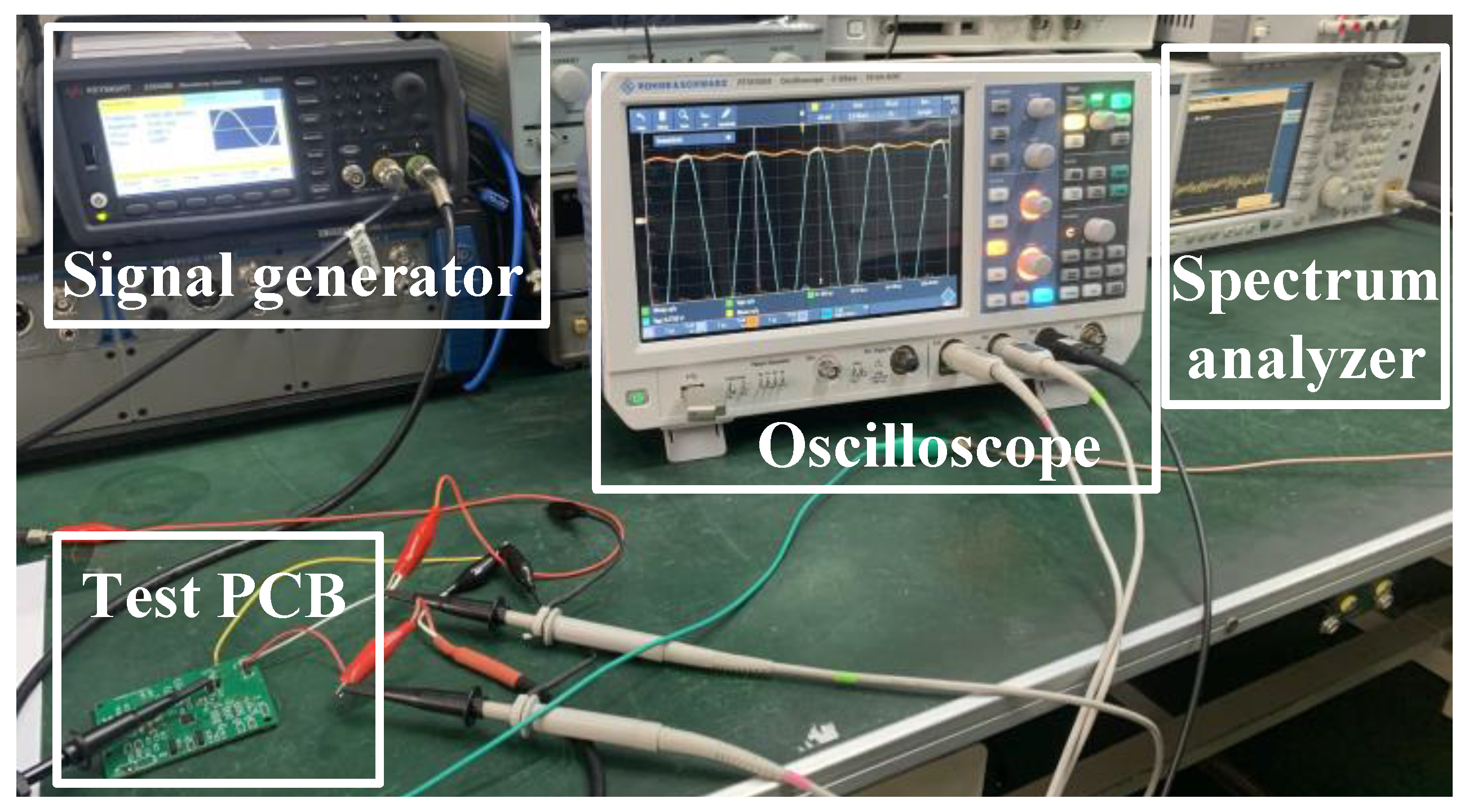
The role of the clock data recovery circuit is to preprocess the data, extract the clock signal, and then provide it to the system. The data preprocessing steps involve differential-to-single-ended conversion and level shifting. Clock extraction consists of edge detection and frequency multiplication. Correct data and accurate clocks are crucial for the overall stability of the system. Therefore, enhancing the reliability of the clock data recovery circuit is of the utmost importance.
Figure 13 shows the block diagram of the clock data recovery circuit. The differential signal C1 is fed into the comparator and level shift circuit, which outputs single-ended data to the passive balise. The level shift circuit reduces the voltage level, thereby decreasing the power consumption of the subsequent circuit. When designing the level shift circuit, it is important to adjust the width-to-length ratio of PMOS and NMOS to 6x and 1x, respectively, which can improve the speed of shifting.
The data are encoded using the differential bi-phase-level(DBPL) code [10], and its coding rules are depicted in Figure 14. Each bit is represented by two states. The first state indicates a phase change, transitioning from +1 to 0, denoted as ‘A’, and from 0 to +1, denoted as ‘B’. The second state is used to compare the current symbol to the previous symbol, with equality represented as ‘1’ and inequality represented as ‘0’. We can utilize the edge extraction circuit and the monostable trigger to extract the clock information. By adjusting the transient state of the monostable trigger through changes in the size of R and C, we can convert the data code, which has a mean rate of 564.48 Kbit/s, into a clock with a mean rate of 564.48 KHz. This clock serves as the reference frequency for the phase-locked loop (PLL), which ultimately generates the required system clock output.

3. Results

In this section, we will present the integration result of the active balise as well as the test results of the designed circuits. This includes the output voltage of the substrate-adaptive rectifier, the output voltage of the BGR–LDO feedback regulator, and the output clock of the clock data recovery circuit. Furthermore, we replaced the designed active balise into the balise system and conducted system testing. The test results are also presented.

3.1. The Integration Result

Figure 15a shows the balise built with discrete components, with the active balise highlighted in the blue box. Based on the integration approach described in Section 2, the integrated active balise designed in this study is shown in Figure 15b. By integrating all the components within the blue box in Figure 15a into a single chip, the use of discrete components was reduced by 25%.
The designed active balise was implemented using the 180 nm HV CMOS process. The total area occupied by these circuits was 1.22 mm × 1.02 mm.
The environment of the test and the photo of the test printed circuit board (PCB) are shown in Figure 16. A signal generator generated the input signal. An oscilloscope was used to observe the waveforms at the output points of the energy extraction circuit, while a spectrum analyzer was used to analyze the output of the clock recovery circuit.

3.2. Energy Extraction Circuit

Using an oscilloscope, we displayed the V i n and V o u t of the substrate-adaptive rectifier, as shown in Figure 17a. The input signal was generated by a signal generator and was a sinusoidal waveform with a peak-to-peak value of 20 V. According to the results, it can be observed that the output voltage of the rectifier remained stable at 9.76 V.
We also displayed the V i n and V o u t of the BGR–LDO feedback structure. When V i n reached about 5 V, V o u t started to rise and eventually stabilized at 3.36 V. Figure 17b shows the oscilloscope display, indicating that the startup circuit was functioning properly and that the stability of the structure was excellent. The initial rise in Vout could potentially be attributed to leakage current.

3.3. Clock Recovery Circuit

According to Section 2.2, the output of the clock recovery circuit should be a 1.128 MHz clock. We used a spectrum analyzer to show the spectrum and phase noise of the output signal from the clock recovery circuit. Figure 18a displays the spectrum of the output clock, indicating that the output clock remained stable at 1.128 MHz. We further tested the quality of the output clock through phase noise analysis, as shown in Figure 18b. We analyzed the phase noise at two points, 1 KHz and 10 KHz offset from the 1.128 MHz output clock, respectively. The results indicated that the phase noise of the output clock was less than −80 dbc/Hz.

3.4. Balise System

The designed energy extraction and data clock recovery circuit chip were integrated into the balise system, as depicted in Figure 19 of the overall PCB. Furthermore, the testing principles by the Eurobalise 085 test specifications are also illustrated in the diagram. The LEU supplied power to the energy extraction circuit through the interface circuit and provided data to the data clock recovery circuit. The energy extraction circuit powered the system, while the clock recovery circuit provided the clock for the balise. After undergoing circuit processing, the data were transmitted to the receiver via an antenna. We used the receiver to test the balise’s mean data rate and maximum time interval error.

3.4.1. Mean Data Rate

The mean data rate test assesses the output data rate of the balise, which is characterized as [10]:
V ¯ = n T ( b i t n ) T ( b i t 0 ) ,
where T ( b i t n ) and T ( b i t 0 ) represent the moments of the n-th bit and 0-bit transitions, respectively, measured in seconds. To ensure accuracy, we conducted a test with 750 bits, and the results are displayed in Figure 20a. The mean data rate deviation was 62 ppm (relative to the center frequency), which significantly exceeded the 200 ppm frequency deviation specified in the European balise test specification.

3.4.2. Maximum Time Interval Error

The maximum time interval error is a commonly used metric to describe a balise’s signal drift [11]. It is defined in international standards as the maximum peak-to-peak time error variation of a given timing signal concerning an ideal timing signal within a particular period. MTIE can be estimated from the formula
M T I E ( n τ 0 ) = m a x 1 k N n ( m a x k i k + n x i m i n k i k + n x i ) ,
where x i is a sequence of N samples of time error function x ( t ) taken with sampling interval τ 0 , τ = n τ 0 is an observation interval, and n can change from 1 to N 1 , depending on the considered values of the observation intervals. We measured the data MTIE of the balise, as shown in Figure 20b. The results show that the maximum time interval was less than 250 ns, which was far beyond the maximum MTIE1 specified in the European balise test specification.

4. Discussion

The test results indicate that our active balise integration solution is suitable for current balise systems. It offers advantages beyond improving integration, reducing the use of discrete components, and enhancing system stability. The test results for the substrate-adaptive rectifier and the BGR–LDO feedback regulator indicate that the balise’s energy efficiency and stability will be improved. That means that the number of balises on the same railway will be reduced, significantly reducing costs. Additionally, the energy extracted by the balise will be more stable. The clock data recovery circuit test results indicate that the balise’s system clock is more accurate. This, in turn, contributes to improving the system’s stability. In the end, we applied the integrated active balise to the system for system testing. The test results further demonstrate that this design effectively enhances the stability of the balise system.
Nevertheless, we believe that further optimization of the balise can be explored from other aspects. Firstly, there is room for integration of the interface circuitry. As shown in Figure 2, this work has integrated the active balise, but the interface circuitry remains built with discrete components. The interface circuitry primarily serves the purpose of signal separation of “C1” and “C6”, but the signal frequencies are low, and the filtering components used are quite large. Therefore, designing an on-chip filter capable of separating low-frequency signals becomes the next step in our work. Secondly, there is potential for integrating passive balises. Similarly, if passive balises are integrated, the number of discrete components will further decrease, resulting in a reduction in the overall system footprint and cost. Thirdly, there is a need for further improvement in system stability. Due to the rapid development of railways, especially the increasing operating speeds of high-speed trains, there is a growing demand for higher stability in railway balises. Therefore, improving the stability of railway balise systems will also become a research objective.

5. Conclusions

This paper proposes a highly integrated and stable railway balise. Our proposal integrates the rectifier, regulator, and clock data recovery circuit, to reduce the use of discrete components, and we designed a BGR–LDO feedback regulator with a limiter-based start-up circuit, to enhance the stability of the system. The test results of the system show that the MDR deviation of the balise was only 62 ppm, which was 69% lower than that specified in the test specification for Eurobalise FFFIS (which is 200 ppm), while the MTIE was less than 250 ns (1000-bit test). Our proposal is suitable for train communication and control, and it will contribute to advancing railway development.

Author Contributions

Conceptualization, Z.L. (Zheng Li) and Q.S.; methodology, Z.L. (Zheng Li), Z.W. and S.H.; software, Z.L. (Zheng Li), Q.S. and J.X.; validation, Z.L. (Zheng Li), Q.S. and Z.W.; formal analysis, Z.L. (Zheng Li); investigation, Z.L. (Zheng Li), Z.L. (Ziming Lin) and F.W.; resources, Z.L. (Zheng Li); writing—original draft preparation, Z.L. (Zheng Li); writing—review and editing, Z.L. (Zheng Li), Y.L. and S.H.; project administration, S.H. and Y.L.; funding acquisition, Z.L. (Ziming Lin) and F.W. All authors have read and agreed to the published version of the manuscript.

Funding

This research was supported by The Laboratory Open Fund of Beijing Smart-chip Microelectronics Technology Co., Ltd.

Institutional Review Board Statement

Not applicable.

Informed Consent Statement

Not applicable.

Data Availability Statement

No new data were created or analyzed in this study. Data sharing is not applicable to this article.

Conflicts of Interest

The authors declare no conflict of interest.

References

  1. System Requirements Specification Chapter 7 ERTMS/ETCS Language, Version 3.4.0; European Union Agency Railways Std: Valenciennes, France, 2014.
  2. FFFIS for Eurobalise, Version 3.0.0; European Union Agency Railways Std: Valenciennes, France, 2012.
  3. Wu, Y.; Wei, Z.; Weng, J.; Deng, R.H. Position Manipulation Attacks to Balise-Based Train Automatic Stop Control. IEEE Trans. Veh. Technol. 2018, 67, 5287–5301. [Google Scholar] [CrossRef]
  4. Rodriguez, L.; Pinedo Zamalloa, C.; López Orbe, I.; Aguado Castrillo, M.; Astorga Burgo, J.; Higuero Aperribay, M.V.; Adin, I.; Bistué, G.; Mendizabal, J. Eurobalise-train communication modeling to assess interferences in railway control signaling systems. Netw. Protoc. Algorithms 2016, 8, 58–72. [Google Scholar] [CrossRef]
  5. Lim, H.W.; Temple, W.G.; Tran, B.A.N.; Chen, B.; Kalbarczyk, Z.; Zhou, J. Data Integrity Threats and Countermeasures in Railway Spot Transmission Systems. ACM Trans. Cyber-Phys. Syst. 2020, 4, 1–26. [Google Scholar] [CrossRef]
  6. Moon, S.; Park, S.; Lee, J.H.; Lee, Y. Rapid Balise Telegram Decoder With Modified LFSR Architecture for Train Protection Systems. IEEE Trans. Circuits Syst. II Express Briefs 2019, 66, 272–276. [Google Scholar] [CrossRef]
  7. Franco, D.; Aguado, M.; Pinedo, C.; Lopez, I.; Adin, I.; Mendizabal, J. A Contribution to Safe Railway Operation: Evaluating the Effect of Electromagnetic Disturbances on Balise-to-BTM Communication in Railway Control Signaling Systems. IEEE Veh. Technol. Mag. 2021, 16, 104–112. [Google Scholar] [CrossRef]
  8. Liu, J.; Cai, B.-G.; Wang, J.; Lu, D.-B. GNSS Jamming Detection and Exclusion for Trustworthy Virtual Balise Capture in Satellite-Based Train Control. IEEE Trans. Intell. Transp. Syst. 2022, 23, 23640–23656. [Google Scholar] [CrossRef]
  9. Gong, S.; Liu, Z.; Luo, L.; Zhou, G.; Wang, S. The optimization study of the on-board antenna of BTM based on electromagnetic model. In Proceedings of the 2013 IEEE International Conference on Intelligent Rail Transportation Proceedings, Beijing, China, 30 August–1 September 2013; pp. 37–41. [Google Scholar] [CrossRef]
  10. Test Specification for Eurobalise FFFIS SUBSET-085. 2012. Available online: https://www.era.europa.eu/system/files/2023-01/sos2_index043_-_subset-085_v300.pdf (accessed on 24 May 2023).
  11. Test Specification for Eurobalise FFFIS SUBSET-036. 2015. Available online: https://www.era.europa.eu/system/files/2023-01/sos3_index009_-_subset-036_v310.pdf (accessed on 24 May 2023).
  12. Dobrogowski, A.; Kasznia, M. Direct approach to MTIE calculation. In Proceedings of the 1999 Joint Meeting of the European Frequency and Time Forum and the IEEE International Frequency Control Symposium (Cat. No. 99CH36313), Besancon, France, 13–16 April 1999; Volume 2, pp. 1121–1124. [Google Scholar] [CrossRef]
  13. Dobrogowski, A.; Kasznia, M. Testing of the methods of real-time MTIE calculation. In Proceedings of the 2005 IEEE International Frequency Control Symposium and Exposition, Vancouver, BC, Canada, 29–31 August 2005; pp. 397–403. [Google Scholar] [CrossRef]
  14. Dobrogowski, A.; Kasznia, M. Some concepts of the real-time MTIE assessment for multi-channel time error measurement. In Proceedings of the 2012 IEEE International Frequency Control Symposium Proceedings, Baltimore, MD, USA, 21–24 May 2012; pp. 1–6. [Google Scholar] [CrossRef]
  15. Raben, H.; Borg, J.; Johansson, J. Improved efficiency in the CMOS cross-connected bridge rectifier for RFID applications. In Proceedings of the 18th International Conference Mixed Design of Integrated Circuits and Systems—MIXDES 2011, Gliwice, Poland, 16–18 June 2011; pp. 334–339. [Google Scholar]
  16. Fu, Q.; Gay, N.; Bansleben, C.; Hildebr, R.; Heiss, M.; Turke, A.; Fischer, W.J. Optimization of the NMOS and PMOS gate cross-connected rectifier for RF power extraction in RFID applications. In Proceedings of the 2008 Asia-Pacific Microwave Conference, Hong Kong, China, 16–20 December 2008; pp. 1–4. [Google Scholar] [CrossRef]
  17. Cha, H.K.; Park, W.T.; Je, M. A CMOS Rectifier With a Cross-Coupled Latched Comparator for Wireless Power Transfer in Biomedical Applications. IEEE Trans. Circuits Syst. II Express Briefs 2012, 59, 409–413. [Google Scholar] [CrossRef]
  18. Jianyun, H.; Yan, H.; Hao, M. High efficient rectifier circuit eliminating threshold voltage drop for RFID transponders. In Proceedings of the 2005 6th International Conference on ASIC, Shanghai, China, 24–27 October 2005; pp. 607–610. [Google Scholar] [CrossRef]
  19. Dhayabarasivam, S.S.; Jayanthi, K. Energy Harvesting Circuit Utilizing MOSFET Based Bridge Rectifier. In Proceedings of the 2018 IEEE International Conference on System, Computation, Automation and Networking (ICSCA), Pondicherry, India, 6–7 July 2018; pp. 1–5. [Google Scholar] [CrossRef]
  20. Grajdeanu, A.-T.; Răducan, C.; Pleşa, C.S.; Neag, M.; Vărzaru, L.; Ţopa, M.D. Fast LDO Handles a Wide Range of Load Currents and Load Capacitors, up to 100 mA and Over 1 μF. IEEE Access 2022, 10, 9124–9141. [Google Scholar] [CrossRef]
  21. Liu, N.; Chen, D. A Transient-Enhanced Output-Capacitorless LDO With Fast Local Loop and Overshoot Detection. IEEE Trans. Circuits Syst. Regul. Pap. 2020, 67, 3422–3432. [Google Scholar] [CrossRef]
  22. Adorni, N.; Stanzione, S.; Boni, A. A 10-mA LDO With 16-nA IQ and Operating From 800-mV Supply. IEEE J. -Solid-State Circuits 2020, 55, 404–413. [Google Scholar] [CrossRef]
  23. Gupta, V.; Rincón-Mora, G.A.; Raha, P. Analysis and design of monolithic, high PSR, linear regulators for SoC applications. In Proceedings of the IEEE International SOC Conference, 2004 Proceedings, Santa Clara, CA, USA, 12–15 September 2004; pp. 311–315. [Google Scholar] [CrossRef]
  24. Heng, S.; Pham, C.-K. A Low-Power High-PSRR Low-Dropout Regulator With Bulk-Gate Controlled Circuit. IEEE Trans. Circuits Syst. II Express Briefs 2010, 57, 245–249. [Google Scholar] [CrossRef]
  25. El-Nozahi, M.; Amer, A.; Torres, J.; Entesari, K.; Sánchez-Sinencio, E. High PSR Low Drop-Out Regulator With Feed-Forward Ripple Cancellation Technique. IEEE J.-Solid-State Circuits 2010, 45, 565–577. [Google Scholar] [CrossRef]
  26. Patel, A.P.; Rincón-Mora, G.A. High Power-Supply-Rejection (PSR) Current-Mode Low-Dropout (LDO) Regulator. IEEE Trans. Circuits Syst. II Express Briefs 2010, 57, 868–873. [Google Scholar] [CrossRef]
  27. Duong, Q.H.; Nguyen, H.H.; Kong, J.W.; Shin, H.S.; Ko, Y.S.; Yu, H.Y.; Lee, Y.H.; Bea, C.H.; Park, H.J. Multiple-loop design technique for high-performance low dropout regulator. In Proceedings of the 2016 IEEE Asian Solid-State Circuits Conference (A-SSCC), Toyama, Japan, 7–9 November 2016; pp. 217–220. [Google Scholar] [CrossRef]
  28. Yu, J.; Zhao, Y.; Wang, Z.; Zhang, T. A curvature-compensated bandgap reference with high PSR. In Proceedings of the 2008 IEEE International Conference on Granular Computing, Hangzhou, China, 26–28 August 2008; pp. 752–755. [Google Scholar] [CrossRef]
  29. Li, W.; Yao, R.; Guo, L. A low power CMOS bandgap voltage reference with enhanced power supply rejection. In Proceedings of the 2009 IEEE 8th International Conference on ASIC, Changsha, China, 20–23 October 2009; pp. 300–304. [Google Scholar] [CrossRef]
  30. Sanborn, K.; Ma, D.; Ivanov, V. A Sub-1-V Low-Noise Bandgap Voltage Reference. IEEE J.-Solid-State Circuits 2007, 42, 2466–2481. [Google Scholar] [CrossRef]
Figure 1. (a) balise transmission system and (b) block diagram.
Electronics 12 04217 g001
Figure 2. Diagram of a balise.
Electronics 12 04217 g002
Figure 3. Diagram of designed energy extraction circuit.
Electronics 12 04217 g003
Figure 4. NMOS and PMOS gate cross rectifier: (a) schematic; (b) input/output voltage.
Electronics 12 04217 g004
Figure 5. Substrate adaptive rectifier: (a) schematic; (b) input/output voltage.
Electronics 12 04217 g005
Figure 6. Comparison of output power.
Electronics 12 04217 g006
Figure 7. Conventional regulator.
Electronics 12 04217 g007
Figure 8. Proposed BGR–LDO feedback regulator.
Electronics 12 04217 g008
Figure 9. Comparison of the PSR of (a) conventional regulator and (b) proposed regulator.
Electronics 12 04217 g009
Figure 10. Simulation result of the PSR.
Electronics 12 04217 g010
Figure 11. Limiter-based start-up circuit.
Electronics 12 04217 g011
Figure 12. Feedback loop of the proposed BGR–LDO feedback regulator.
Electronics 12 04217 g012
Figure 13. Clock data recovery circuit.
Electronics 12 04217 g013
Figure 14. Coding rule of DBPL.
Electronics 12 04217 g014
Figure 15. The integration result: (a) the active balise before being integrated; (b) the microscope photograph of the integrated active balise.
Electronics 12 04217 g015
Figure 16. Test environment and the PCB.
Electronics 12 04217 g016
Figure 17. The results of the energy extraction circuit: (a) input and output voltage of the substrate-adaptive rectifier. (b) Vin and Vout of the BGR–LDO feedback structure.
Electronics 12 04217 g017
Figure 18. The results of the clock data recovery circuit: (a) spectrum of the output clock; (b) phase noise of the output clock.
Electronics 12 04217 g018
Figure 19. PCB of balise system and test diagram.
Electronics 12 04217 g019
Figure 20. The results of the balise system: (a) mean data rate of the output; (b) MTIE results.
Electronics 12 04217 g020
Disclaimer/Publisher’s Note: The statements, opinions and data contained in all publications are solely those of the individual author(s) and contributor(s) and not of MDPI and/or the editor(s). MDPI and/or the editor(s) disclaim responsibility for any injury to people or property resulting from any ideas, methods, instructions or products referred to in the content.

