Article

An Asymmetrical 19-Level Inverter with a Reduced Number of Switches and Capacitors

Department of Electrical Engineering, Aliabad Katoul Branch, Islamic Azad University, Aliabad Katoul 4941793451, Iran
*
Author to whom correspondence should be addressed.
Electronics 2023, 12(2), 338; https://doi.org/10.3390/electronics12020338
Submission received: 30 October 2022 / Revised: 25 November 2022 / Accepted: 7 December 2022 / Published: 9 January 2023

Abstract

:
Multilevel inverters are able to provide loads with voltages of high power quality using several DC sources, capacitors, switches, and diodes in their structures. However, the usage of the higher number of semiconductor devices (switches and diodes) and capacitors causes an increase in losses and costs and decreases their efficiency. Thus, lowering the number of switches and capacitors is a challenging issue in designing a multilevel inverter. In this paper, an asymmetrical multilevel inverter is proposed that produces 19-level output voltages. The circuit is composed of nine switches, six diodes, two capacitors, and two isolated DC sources. In comparison with other topologies, the most important advantage of the introduced 19-level topology is the usage of a lower number of switches and capacitors, which leads to a decrease in the number of gate drivers and the total volume of the system. During the charging process, capacitors never connect to each other in series, i.e., they are self-balancing and do not require the extra circuits. The proposed topology offers a total harmonic distortion (THD) of 7.4% in the output voltage, which is less than 8%, complying with the IEEE standards. The performance of the topology is validated under various load conditioning through an experimental setup in the laboratory.

1. Introduction

The multilevel inverter (MLI) is one type of power electronic converter used for medium voltages and high-power applications. Compared to the two-level inverters, it is able to provide voltages with low total harmonic distortion (THD), low voltage rating on the semiconductor devices, and high power quality for the load. In MLIs, the switching frequency of switches can be reduced, which leads to a decrease in the power losses of the semiconductor devices and an increase in the efficiency of the inverter [1,2,3]. There are three basic topologies of MLIs: Neutral Point Clamped (NPC) [4], Flying Capacitor (FC) [5], and Cascade H-Bridge (CHB) [6,7]. One important advantage of NPC and FC topologies is that they use just one isolated DC source in their structures. However, to provide a higher number of voltage levels in the output, they need more switches (Nsw), diodes (Nd), and capacitors (NC). For instance, to provide a load with 5-level voltages, NPC and FC topologies require the numbers (Nsw, Nd, and NC), respectively, to be equal to (8, 6, 4) and (10, 0, 8). Another drawback of the NPC and FC topologies is neutral point balancing, which involves using an extra circuit. To overcome these issues, numerous types of research have been conducted; nonetheless, the proposed designs still suffer from large numbers of devices in their structures [8,9]. The CHB-based topologies of MLIs have been developed due to the modularity of their structures, fewer capacitors, and simple controllability. They have been widely used for photovoltaic systems, rechargeable batteries, electrical vehicles, reactive power compensators, and so forth [10,11,12]. The CHB topology can be configured in asymmetrical mode (inequality of input DC sources) to achieve more voltage levels. The main disadvantage of CHB topologies is the usage of several isolated DC sources in their structures. Recently, the proposed switched-source (SS)- and switched-capacitor (SC)-based topologies have reduced the number of devices. The SC configurations can play the role of the boost converter for photovoltaic applications [13]. Generally, in SS and SC structures, to achieve a higher number of voltage levels, and lower THD on the load, the number of DC sources and capacitors should be increased [14,15]. However, compared to the NPC and FC topologies, they benefit from a lower number of switches and diodes [16,17]. In [18], a multilevel inverter topology was introduced with a very low number of switches. However, the total standing voltage (TSV) of the proposed inverter was equal to 9. In [19], a new multilevel inverter structure was presented by Babaei with 10 switches and 3 DC sources to obtain the 13-level output voltage. The introduced multilevel inverter topology in [20] had 14 switches and 2 capacitors. This topology had a high number of switches but the TSV was 5.33. From the above discussion, it can be concluded that by decreasing the number of switches, the TSV increases and vice versa. Hence, a multilevel inverter topology can be designed with a low number of switches and satisfy the value of TSV. This paper presents an asymmetrical 19-level hybrid switched source-capacitor inverter that has the ability to provide the merits of SS and SC topologies. The proposed structure consists of nine switches, six diodes, two capacitors, and two isolated DC sources, which act as the boost converter with a voltage gain of 2.25. The number of switches, gate drivers, and capacitors in the proposed 19-level topology is very low and comparable with the recently suggested topologies. However, the TSV of the topology is 7.2, but this is satisfied in comparison with other structures such as [18]. Multi-carrier pulse width modulation (MC-PWM) is chosen as the switching strategy because it features the multilevel inverter as a controllable apparatus.
The paper is organized as follows. In Section 2, the proposed topology is presented, accompanied by a description of the performance of the switches. The generalized topology is illustrated in Section 3. Section 4, Section 5 and Section 6, respectively, present a comparison of the proposed multilevel inverter with other topologies, detail the MC-PWM scheme, and conduct calculation of the losses and efficiency, respectively. To verify the performance of the inverter, the results of the laboratory tests are given in Section 7. Finally, Section 8 concludes the paper.

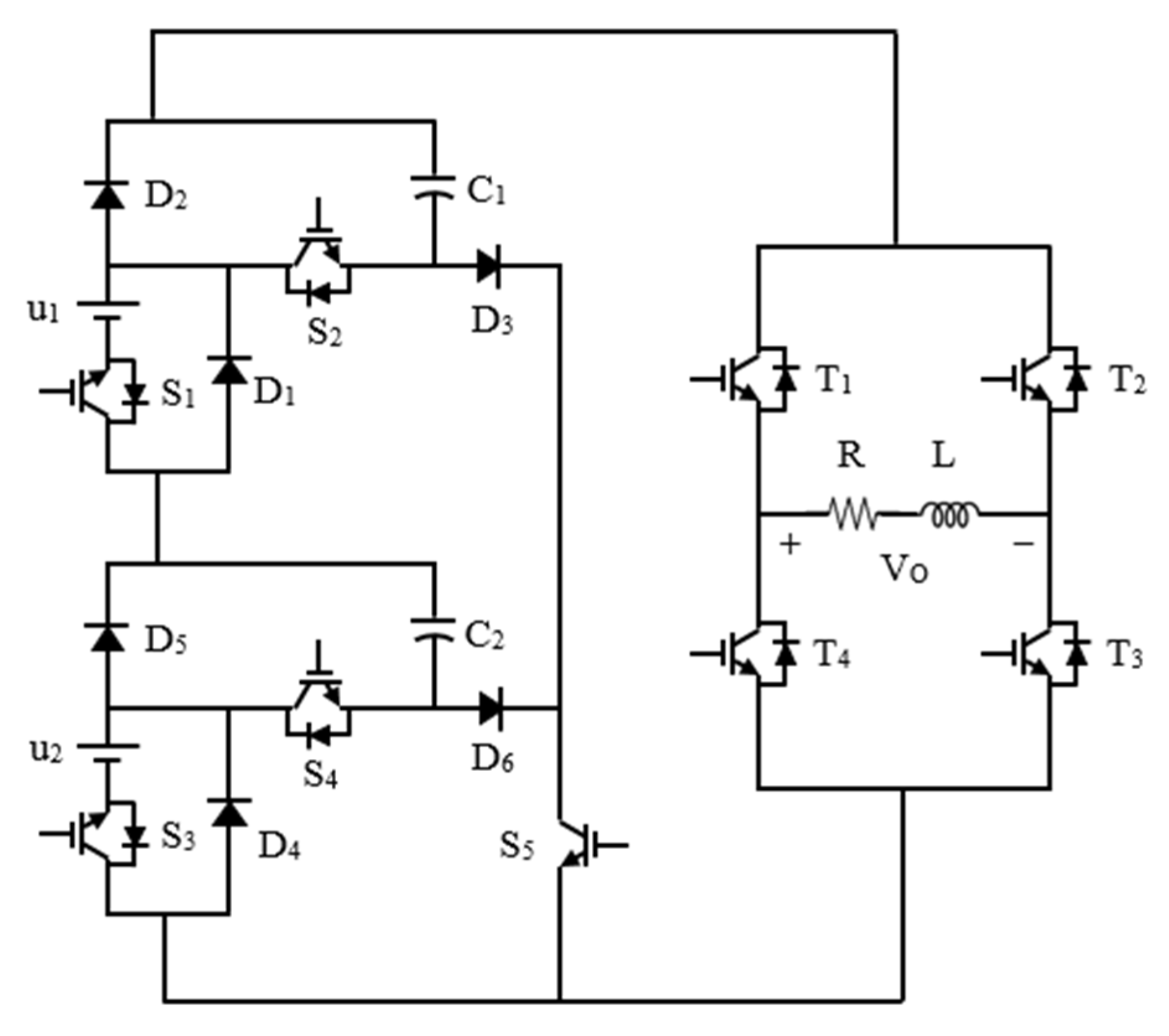
2. Proposed 19-Level Inverter

Figure 1 shows the proposed asymmetrical 19-level inverter. It consists of two units, nine switches, two capacitors, six diodes, and two DC sources. Switch S5 is only applied to charge capacitors C1 and C2. In addition, pairs of switches (S1, S3) and (S2, S4) are assigned to deliver the voltage of the DC sources and capacitors to the load, respectively. The steps of magnitude of the DC sources are introduced as u1 = 3 V and u2 = V. In other words, if we choose V = 20 v, the first and second input DC bus sources are set at u1 = 60 v and u2 = 20 v, respectively. Because the maximum voltage level on the load is 9 V, the magnitude of output voltage of the inverter is 180 V. Assuming the values of DC sources as u1 = 3 V and u2 = V, supposedly in asymmetrical conditions, capacitors C1 and C2 would be charged up to 4 V and 1 V, respectively. Thus, the four available voltage sources V, V, 3 V, and 4 V can give rise to a 19-level voltage on the output of the inverter. It should be noted that switch S5 must have no body diode, due to the unidirectional flow of the current responsible for charging the capacitors. The switching states of the proposed 19-level inverter are listed in Table 1. In order to create more frequent capacitor charging, the zero voltage level is bisected into two parts (0+, 0−) according to states 10 and 11. As the capacitors are charged by only one switch (S5) simultaneously, there are only four switching states through which the capacitors are charged. Hence, the discharging time of the capacitors is expected to be longer than the charging time. To overcome the issue, each unit must have a separate switch to charge its capacitor, which leads to increasing the number of switches. As a result, in order to avoid this effect, there must be only one common switch (S5) to charge the capacitors. However, this issue, again, leads to simultaneous charging of the capacitors, which, in turn, causes the discharging time of capacitors to be larger than their charging time. Figure 2 shows the circuit configuration and paths of the current flow during the positive and zero levels of operation.
For instance, in Figure 2a, which describes state 1 of Table 1, when switches S1, S2, S3, and S4 are turned on, diodes D1, D2, D4, and D5 are in reversed bias. In these conditions, the current passes through devices S3, u2, S4, C2, S1, u1, S2, C1, T1, load, and T3, which, in turn, produces a +9 V level across the output. Other schematics can be analyzed in the same way.

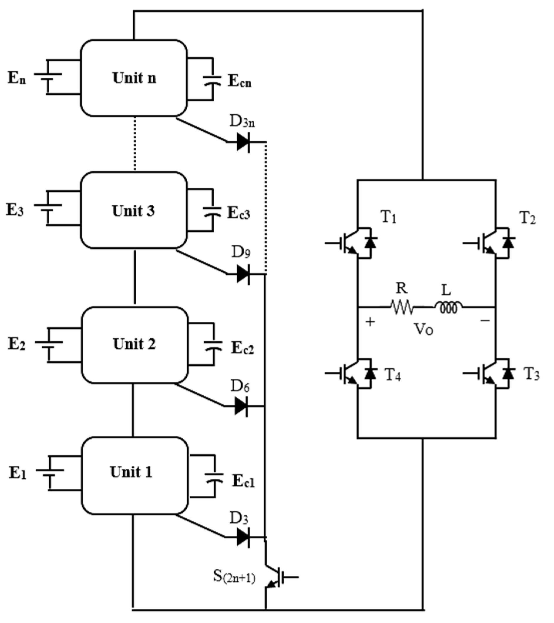
3. The Proposed Generalized Multilevel Inverter

If devices u1, S1, S2, D1, D2, and C1 form a unit, the structure of the proposed 19-level inverter, shown in Figure 1, would consist of two units. As shown in Figure 3, in order to achieve more voltage levels, more units can be utilized. In such cases, based on the values of DC sources, several asymmetrical modes can be defined for the proposed multilevel inverter. The first, second, and third asymmetrical modes are assumed to be (V, 2 V, 3 V, …, nV), (V, 3 V, 5 V, …, (2n−1) V), and (V, 3 V, 10 V, 34 V, …), respectively. Although the third asymmetrical mode produces a higher number of voltage levels than the first and second ones, in this case, the total standing voltage (TSV) increases in some switches, which necessitates the usage of switches with higher rated voltage; this, in turn, causes higher costs. For the case of n units, the number of devices needed for the three aforementioned asymmetrical modes can be written as
{ N C = n , n Ν N s w = 2 n + 5 , n Ν N d = 3 n , n Ν
where NC, Nsw, and Nd are the number of capacitors, switches, and diodes, respectively. According to Figure 3, in the third asymmetrical mode, values of the DC-source and capacitor voltages of unit n can be obtained as
{ E n = i = 1 n 1 E i + i = 1 n 1 E c i + 1 E c n = i = 1 n E i
The relationship between the number of required devices and the voltage levels is listed in Table 2. For example, to reach the 33-level voltages across the load, we need 11 switches, 9 diodes, 3 units, 3 capacitors, and 3 DC sources; these numbers account for only the first asymmetrical mode.

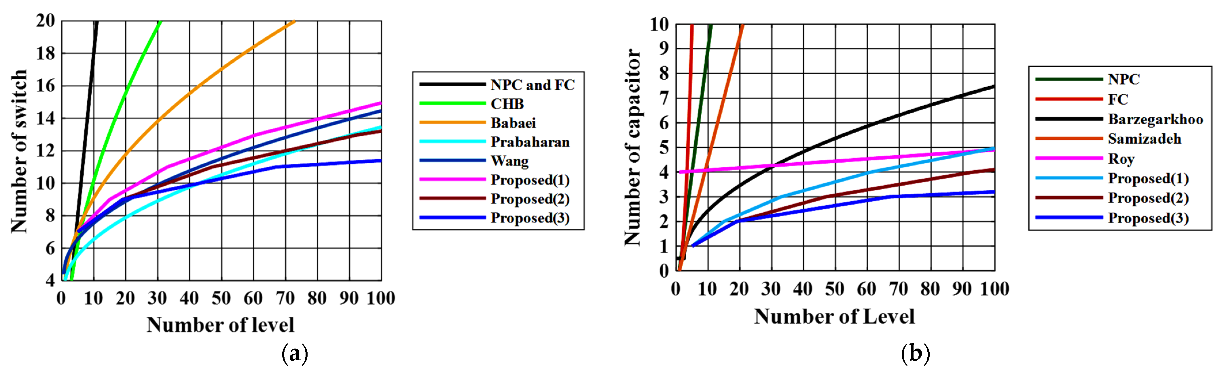
4. Comparison of the Proposed Multilevel Inverter with Other Topologies

The suggested multilevel inverter can be weighed up against other topologies in terms of the number of required switches and capacitors. Here, the NPC, FC, CHB, Prabaharan [18], Babaei [19], Wang [20], Barzegarkhoo [21], Samizadeh [22], and Roy [23] structures are chosen to be compared with the proposed configuration, as demonstrated in Figure 4.
According to Figure 4a, the Prabaharan topology has the lowest number of switches as the number of voltage levels at the output are less than 84 (in point M), but when the number of voltage levels exceeds 84, this topology is outperformed by the proposed structure; that is, the proposed structure offers the minimum number of required switches among all the designs. However, this phenomenon occurs in the second asymmetrical mode, i.e., V, 3 V, 5 V, …, (2n−1) V. On the other hand, as illustrated in Figure 4b, the suggested topology needs the lowest number of capacitors, both in the first and second asymmetrical modes. Therefore, as a result of the comparisons, the proposed inverter is able to produce a high number of voltage levels for the load by the low number of switches and capacitors. Nonetheless, more output voltage levels can be achieved at the cost of higher TSVs.
Table 3 shows the comparison of the proposed configuration with other topologies. According to this table, the 19-level proposed inverter has the lower number of switches and gate drivers than other conventional structures. Moreover, the voltage gain of the introduced topology is 2.25, which is more than the other studied topologies. However, it seems that the TSV of the proposed inverter is higher than those of the other topologies [18]. This is because the introduced multilevel inverter works at the asymmetrical mode with u1 = 3 V and u2 = V, which leads to an increase in the stress voltage of semiconductor devices.

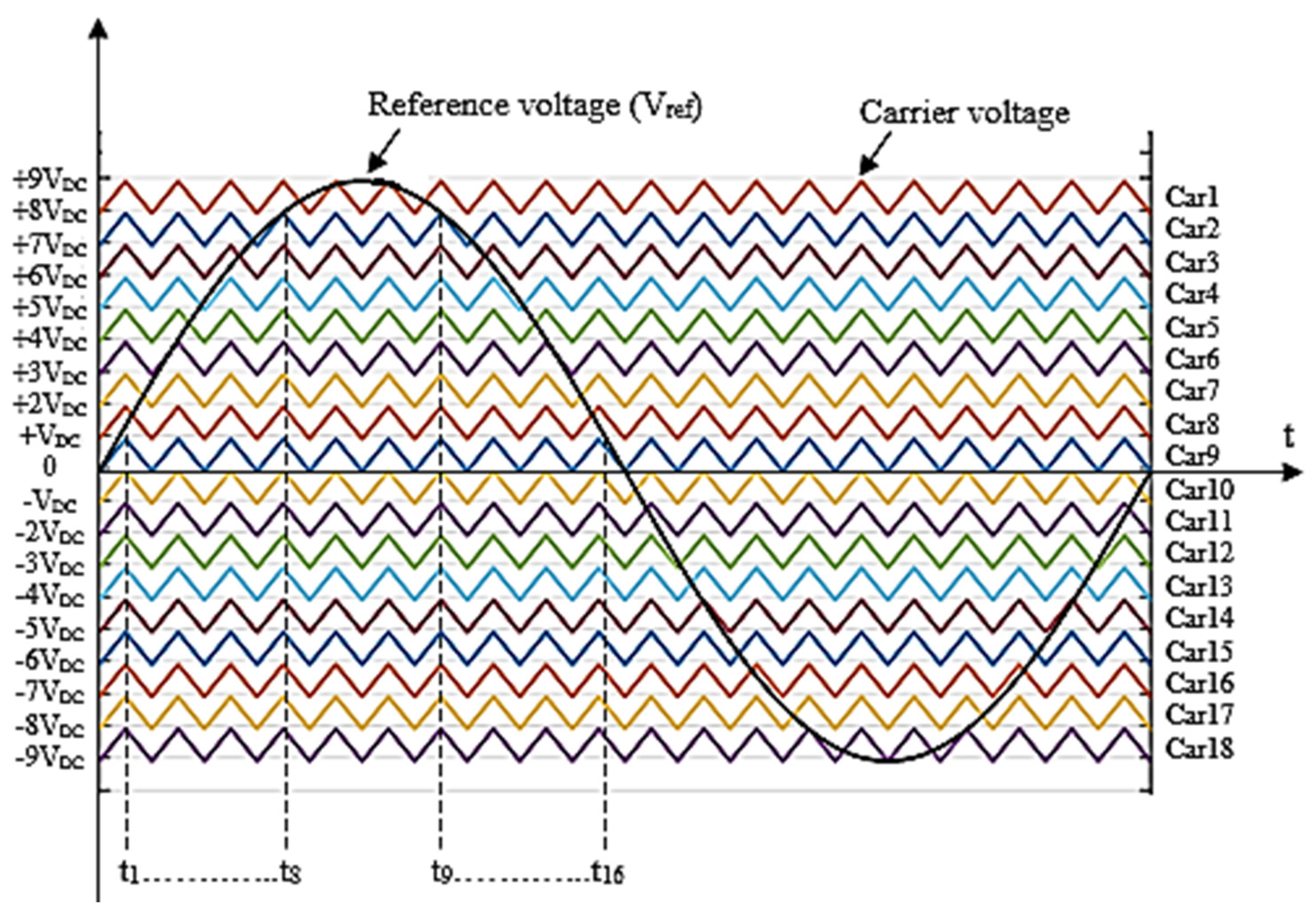
5. Multi-Carrier Pulse Width Modulation Technique

According to Figure 5, in the MC-PWM switching technique, in order to produce the 19-level voltage at the MLI output, we need one sinusoidal 50 Hz reference signal with amplitude Aref and frequency fref, 18 triangular carrier signals, and 20 switching states. As shown in Figure 5, all of the carrier signals have the same amplitude (At) and frequency (fsw), but they are shifted up and down relative to each other based on the applied VDC.
According to this figure, in the positive half-cycle, the carrier signals car1, car2, car3, …, and car9 are responsible for the generation of the positive voltage levels, which provide the switching pulses for all the switches except T2 and T4. Similarly, in the negative half-cycle, the carrier signals car10, car11, car12, …, and car18 are responsible for the generation of the negative voltage levels, which provide the switching pulses for all the switches except T1 and T3.

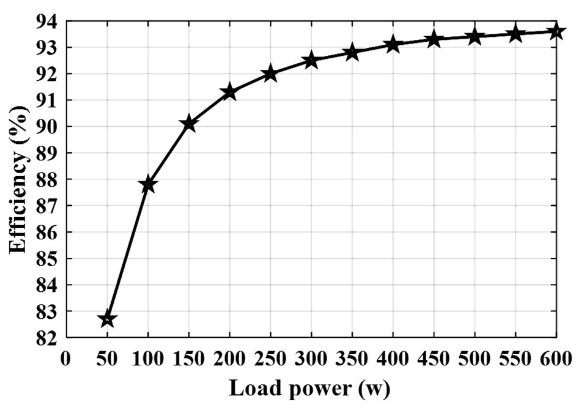
6. Calculation of Losses and Efficiency

In the proposed MLI, the losses consist of three parts: the capacitor charging losses (Ploss, cap), the switching losses (Psw), and the conducting losses (Pcond).

6.1. The Capacitor Charging Losses

The capacitor charging losses are divided into the capacitor ripple losses (Pc, ripple) and the conduction losses of the capacitor (PCC). The capacitor ripple losses, which occur due to voltage differences between the dc input and the voltage across the capacitors, are obtained by [24,25,26]:
P c , r i p p l e = f r e f 2 k = 1 2 C k Δ V C k 2
where ΔVCk is the voltage ripple of kth capacitor, which can be written as
Δ V C k = 1 C k t a , k t b , k i c k ( t ) · d t
where iCk is the current flowing through the kth capacitor. In addition, the conduction losses of the capacitor, which are created by the internal resistance of capacitors (RC), can be described as
P C C = ( 2 π f r e f π ) k = 1 2 t a , i t b , i R C i c k 2 · d t
Finally, the capacitor charging losses are calculated as
P l o s s , c a p = P C , r i p p l e + P C C

6.2. The Switching Losses

The switching losses are rooted in the existing delay between changing the states of the switch from on to off and vice versa. These losses, present in switches and diodes, are the reason that creates the so-called switching losses in the proposed MLI. Therefore, a faster switch or diode in terms of recovery time evidently has lower switching losses. The switching losses during the ON (Psw,on) and OFF (Psw,off) states of a typical switch can be calculated by (7) and (8), respectively [26]:
P s w , o n = f s · V o f f · I o n · t o n 6
P s w , o f f = f s · V o f f · I o n · t o f f 6
where ton and toff are the time intervals during which the switch turns on and turns off, respectively, fs is the switching frequency, Voff is the voltage rating of the switch, and Ion is the average load current. Similarly, the switching losses of a diode can be calculated as
P s w , D = f s · V R M · I R M · t B 6
where VRM and IRM are the maximum voltage and current of reverse recovery, respectively, and tB is the delay time of the reverse current. The total switching losses, then, can be formulated as follows:
P s w , t o t a l = i = 1 N s w ( j = 1 N o n ( P s w , o n , i j ) + j = 1 N o f f P s w , o f f , i j ) + k = 1 N d ( h = 1 N o f f ( P s w , D , k h ) )
where Non and Noff are, respectively, the numbers of ON and OFF states of the switches and diodes during a complete fundamental cycle (1/Ts).

6.3. The Conducting Losses

Two key factors are the main causes of the conducting losses. One is the internal resistance of each semiconductor device and the other is the voltage of their ON state. These together create the voltage drop on the semiconductor devices. The conducting losses on a switch (Pcond,sw) and diode (Pcond,D) can be written as [27]
P c o n d , s w = V o n , s w · I s w , a v e + R o n , s w · I s w , r m s 2
P c o n d , D = V o n , D · I D , a v e + R o n , D · I D , r m s 2
where Von and Ron are the voltage and resistance of the switch and diode during the ON state, respectively. In addition, Irms and Iave are the RMS and average current of the semiconductors, respectively. In MLIs, each voltage level creates a conducting loss. For example, according to Figure 2, in steps +(8, 9) VDC, the conduction losses can be obtained using [28,29,30]
P c o n d , ( + 9 V ) = ( 6 V o n , s w · I l o a d , a v e + 6 R o n , s w · I l o a d , r m s 2 ) + ( 0 × V o n , D · I l o a d , a v e + 0 × R o n , D · I l o a d , r m s 2 )
P c o n d , ( + 8 V ) = ( 5 V o n , s w · I l o a d , a v e + 5 R o n , s w · I l o a d , r m s 2 ) + ( 1 × V o n , D · I l o a d , a v e + 1 × R o n , D · I l o a d , r m s 2 )
For the purpose of clarification, notice that in step +8 V, according to Figure 2b, there are five switches and one diode in the current commutation path. Therefore, the equation for the corresponding conduction losses of this step must account for five switches and one diode. The calculation of the conducting losses for the other steps follows a similar procedure. The total conduction losses, then, are the sum of losses of all the steps, which is
P c o n d , t o t a l = P c o n d , ( + 9 V ) + P c o n d , ( + 8 V ) + P c o n d , ( + 7 V ) + + P c o n d , ( 7 V ) + P c o n d , ( 8 V ) + P c o n d , ( 9 V )
Accordingly, the efficiency of the proposed 19-level topology can be calculated as
η = ( P o u t P o u t + P l o s s ) × 100 = ( ( V o u t ( r m s ) ) 2 R l o a d ( V o u t ( r m s ) ) 2 R l o a d + P l o s s , c a p + P s w , t o t a l + P c o n d , t o t a l ) × 100
Figure 6 illustrates the efficiency curve as load power changes. As can be seen from the figure, in lower powers, the efficiency is low due to the small amplitude of the load current. However, as the load power rises up, the efficiency increases too until it reaches the maximum value, which is equal to 93.6% for the proposed 19-level inverter.

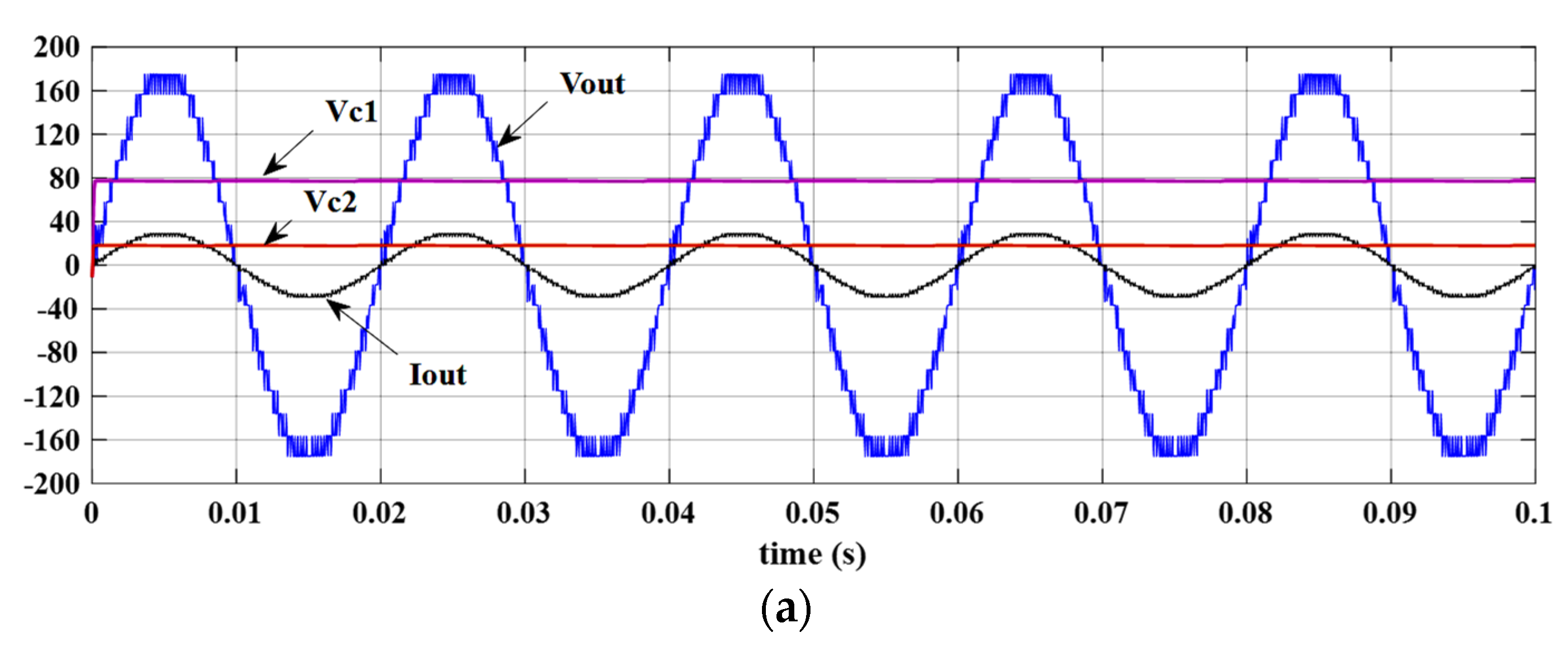
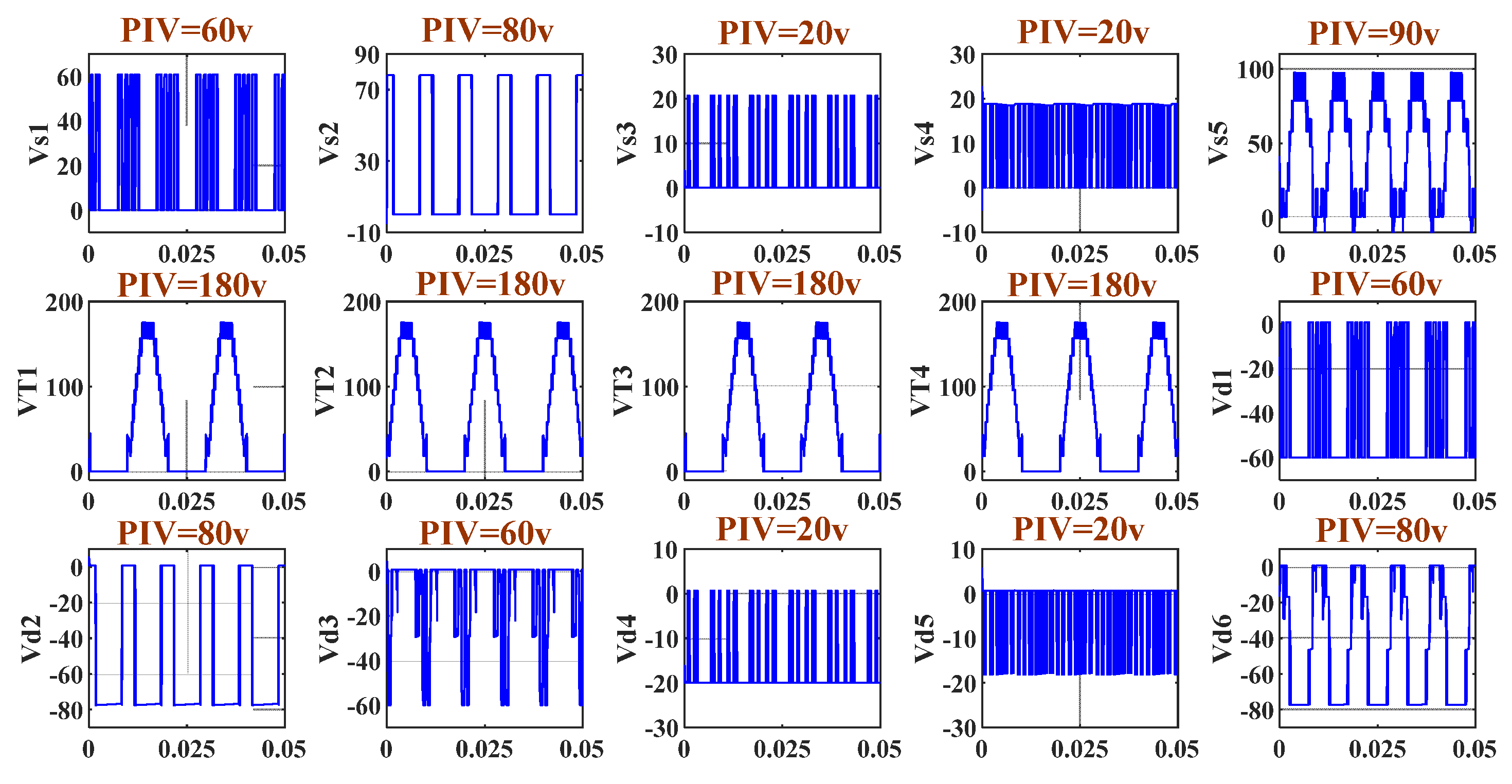
7. Simulation and Experimental Results

7.1. Simulation Results

In order to validate the performance of the proposed 19-level inverter, several simulations are carried out using SIMULINK/MATLAB. The DC bus voltages u1 and u2 are set at 60 V and 20 V, respectively. The switches and diodes are modeled as similar to semiconductor devices applied to the laboratory. For example, the inner resistance and voltage drop of switches and diodes are set at (0.07 Ω, 1.2 v) and (0.065 Ω, 0.85 v), respectively. Moreover, the values of both capacitors C1 and C2 are arranged as 4700 µF. Figure 7 shows the simulation results for output voltage, output current, and capacitor voltages. As shown in Figure 7, the output voltage forms a 19-level waveform under the MC-PWM switching strategy. In addition, the capacitor voltages of C1 and C2 are close to 80 V and 20 V, respectively, which comply with the values of (u1 + u2) and u2, respectively. Hence, the capacitors are charged up to 4 V and 1 V according to the presented discussion in Section 2. Figure 7b shows the results with the increase in the load from Z = 300 Ω to Z = 150 Ω at t = 0.05 s. It can be seen from this figure that the current magnitude increases as 2 times. In Figure 7c, the load changes from pure resistive to inductive-resistive conditions. For this reason, the current wave is closed to sinusoidal form. In Figure 7d,e, the modulation index decreases from m = 1 to m = 0.5. In these conditions, the output voltage varies from a 19-level to 11-level form. This is because with m = 0.5, the reference voltage shown in Figure 5 decreases as much as half its previous value. Thus, in this case, the reference voltage is compared to 10 carrier waves instead of 18 carrier waves. It can be concluded from Figure 7 that the transient states of the proposed 19-level inverter have a fast response with the change in the load and modulation index. Figure 8 shows the voltage of switches and diodes applied to the proposed 19-level inverter. These voltages present the peak inverse voltage (PIV) of each switch and diode.
It can be seen from Figure 8 that, among the semiconductor devices, the switches and diodes, S3, S4, d4, and d5, have lower stress voltages than the others because they are arranged inside the small DC bus voltage u2 = 20 V (see Figure 1). According to Figure 8, the sum of the PIV of switches and diodes is equal to 1310, which is called the TSV. By dividing the TSV by the maximum voltage level on the load (180 v), the TSVpu is obtained as 1310/180 = 7.2, which complies with Table 3.

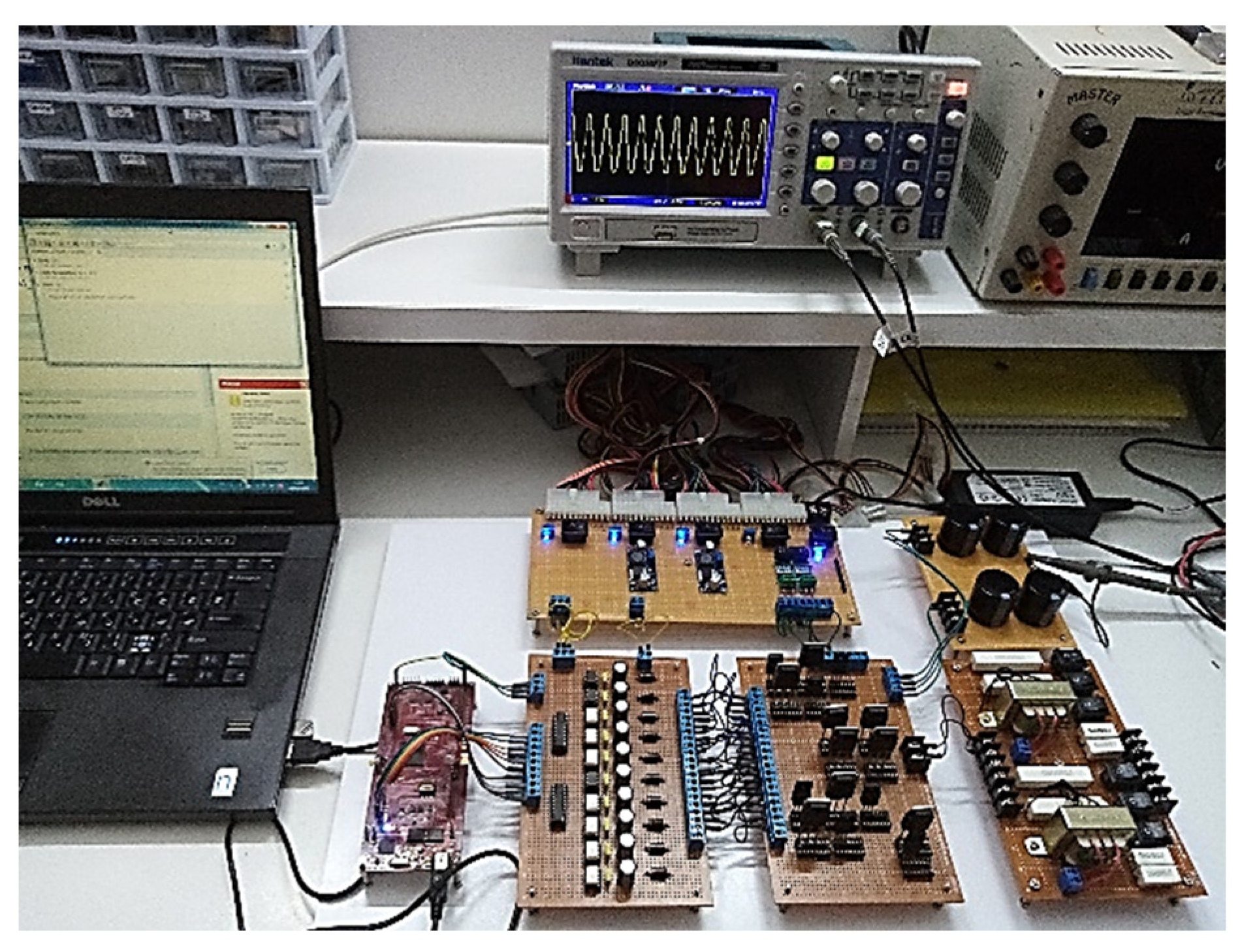
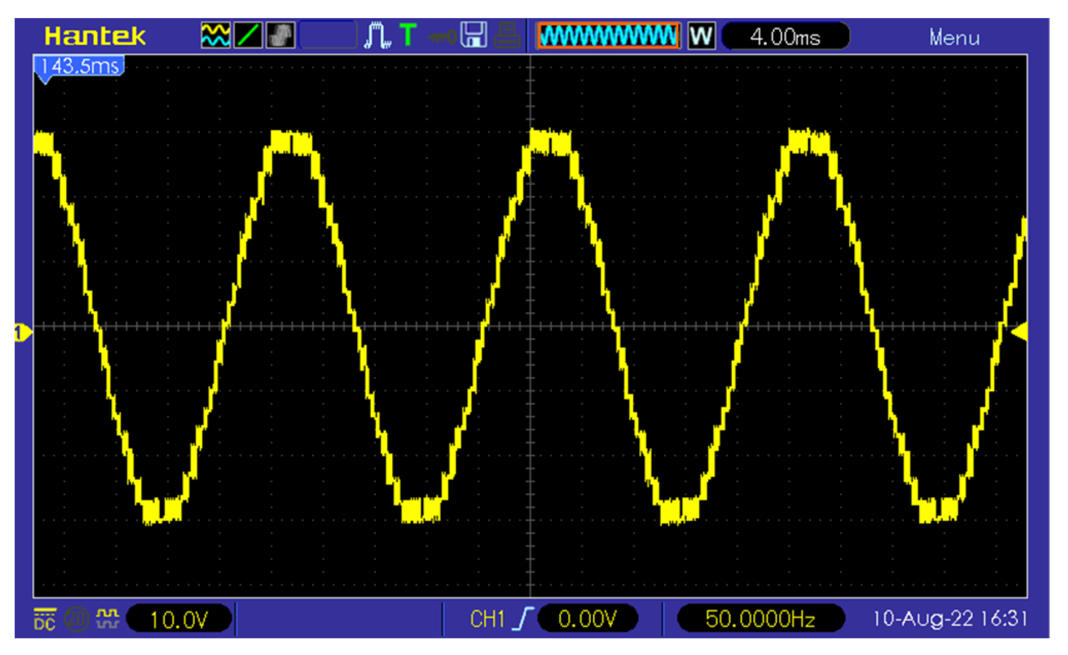
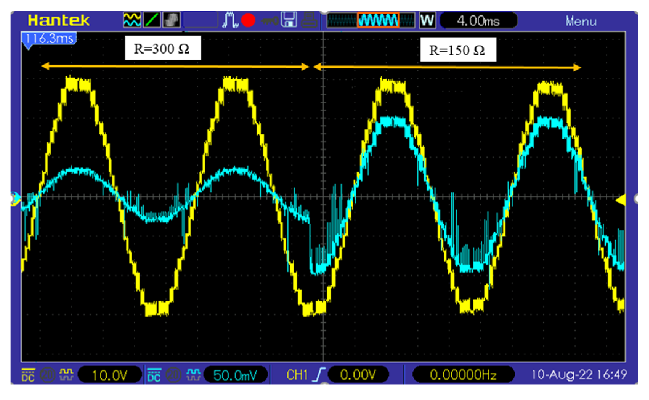
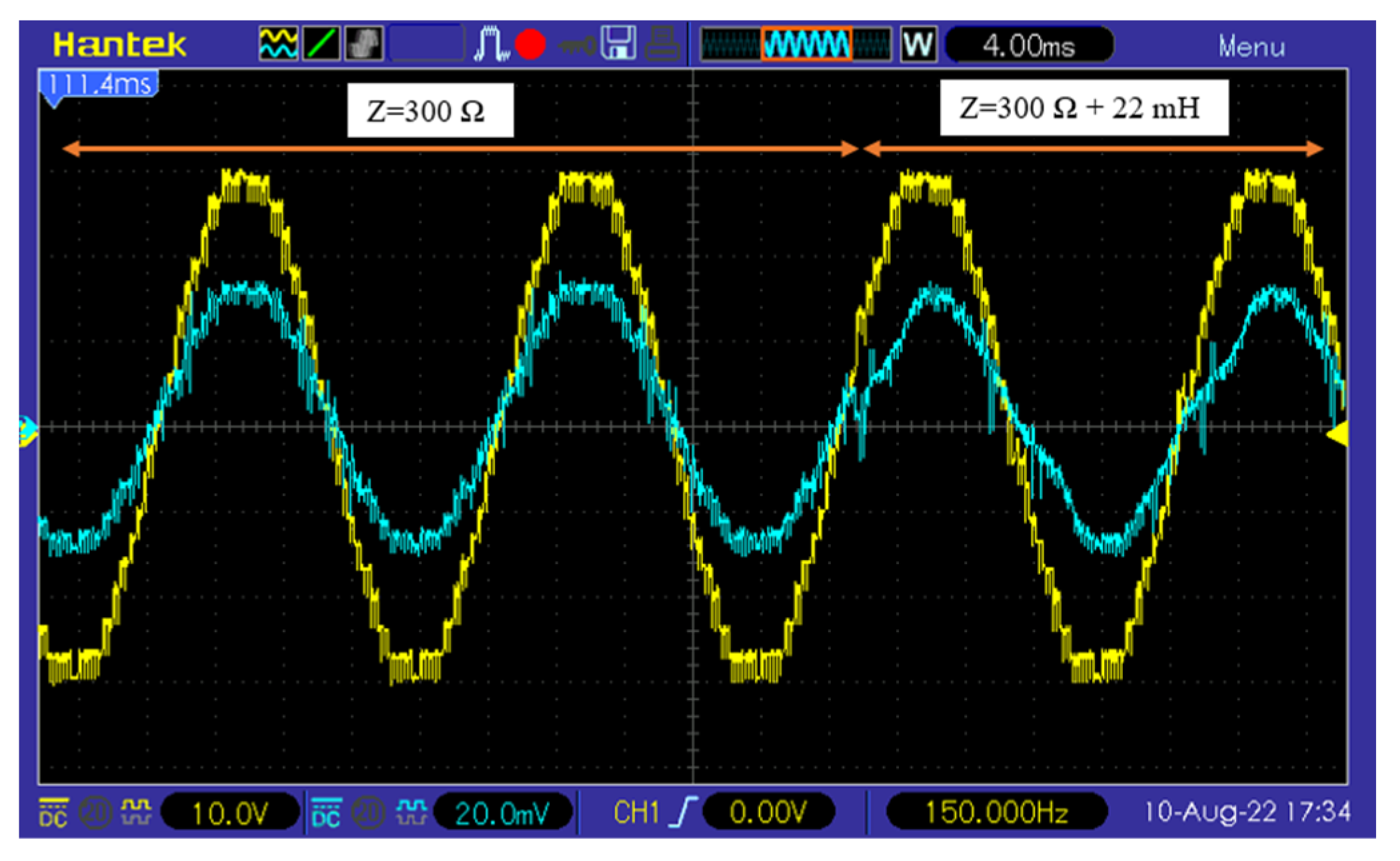
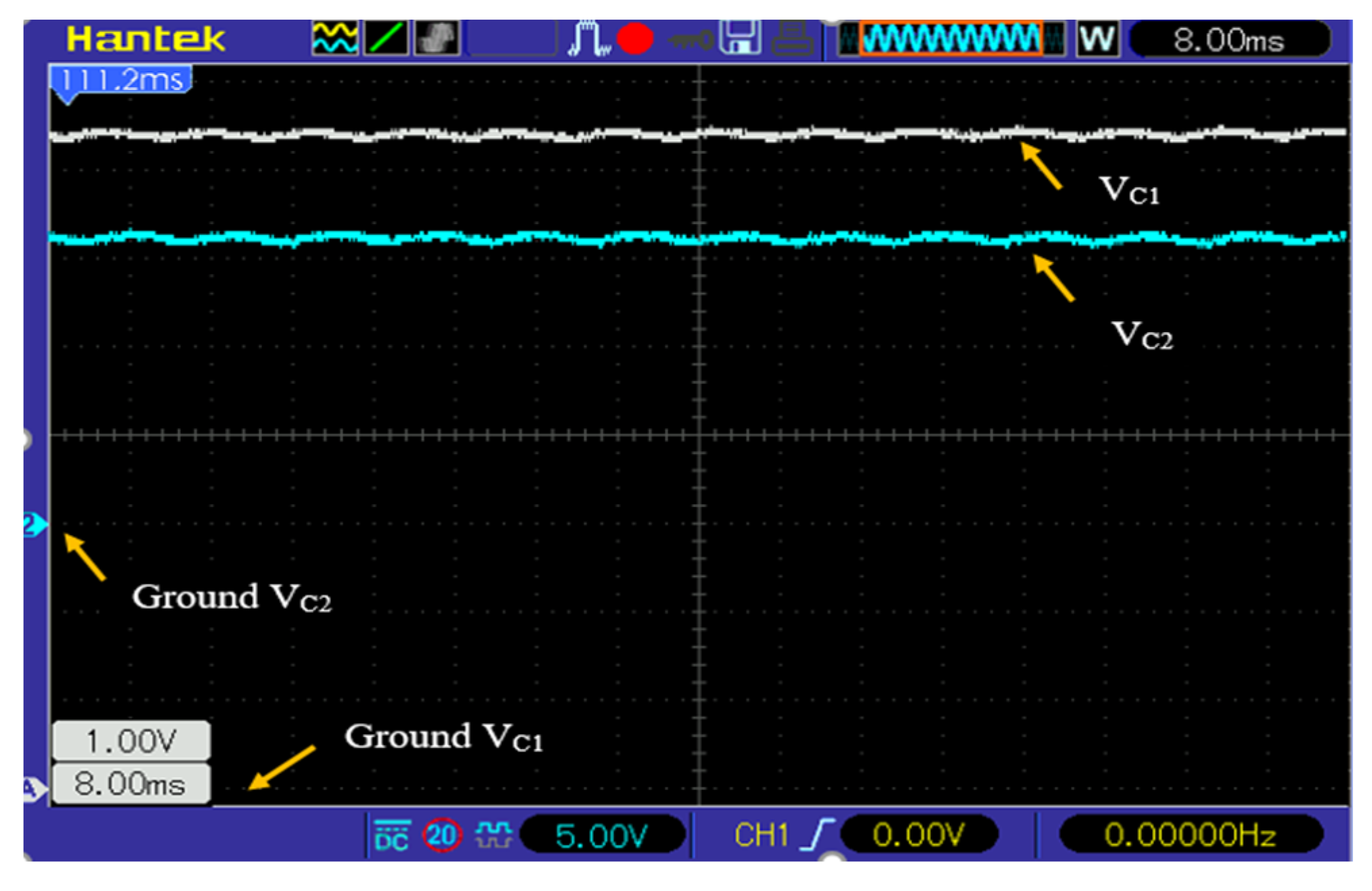
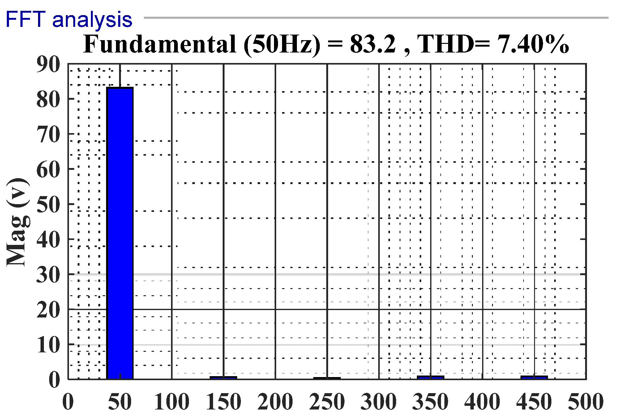
7.2. Experimental Results

To assess the simulation results, an experimental setup is implemented using the TMS320F28379D DSP. Figure 9 shows the prototype setup, which includes a DSP, a gate driver, the proposed 19-level inverter, several power supplies, and different resistive-inductive loads. In the gate driver circuit, the HCPL-3120 is used both as a DSP ground isolator and as a switch driver; this needs a power supply of +15 V with the ground (GD). In addition, in the gate driver circuit, the 74HC245 buffer is applied to prevent current consumption by the DSP. In this setup, the switches and diodes are the FGA25N120 IGBT and MBRF20100CT SCHOTTKY diode, respectively. However, within the laboratory environment, it is better to use a low-voltage drop switch such as the STGW50HF60SD IGBT due to limitations in the ranges of available DC voltage sources.
Generally, due to the technical limitations encountered in implementations, in the context of our multilevel inverter, a few important points need to be stated:
(1)
All gate driver power supplies should be isolated from each other.
(2)
The reference signal in the MC-PWM (see Figure 5) must be set on the sample base mode with 1000/5 samples per period and a sample time of 0.0001 s.
(3)
A high-power resistor should be applied parallel to each capacitor for discharging their voltage when the test is completed.
The parameters related to the laboratory implementation are listed in Table 4. Figure 10 shows the 19-level output voltage with an amplitude of 150 V. According to the smallest selected voltage level, i.e., 20 V, the maximum voltage level was expected to be 180 volts, but due to the voltage drop across the switches and diodes, this value descends to 150 volts.
Figure 11 depicts the output voltage and current of the 19-level inverter when the resistive load changes from Z = 300 Ω to Z = 150 Ω. As shown in Figure 11, the amplitude of the current changes from I = 0.4 A to I = 1 A. Figure 12 shows the output voltage and current when the load changes from pure resistive Z = 300 Ω to Z = 300 Ω + 22 mH. According to Figure 12, the current approximately mimics a sinusoidal waveform with a peak of 0.4 A. Figure 13 depicts the voltages of the capacitors. According to this figure, capacitors C1 and C2 are charged up to about 75 V and 16 V, respectively. Given the values of the DC sources as u1 = 60 v and u2 = 20 v, capacitors C1 and C2 were expected to charge up to 80 V and 20 V, respectively. The difference is, again, due to the voltage drop across the switches and diodes. Under a pure resistance load, the frequency spectrum of the harmonic curve is depicted in Figure 14. According to this figure, the THD in the output of the inverter is 7.4%, which is less than 8%, complying with the IEEE standards.

8. Conclusions

In this paper, a 19-level inverter was proposed, which consisted of nine switches, six diodes, two capacitors, and two isolated DC sources. The main advantage of the proposed inverter was the utilization of a very low number of switches and gate drivers compared to other suggested structures. The voltage gain of the proposed inverter was 2.25. The THD of the output voltage achieved 7.4%, which is less than 8%, complying with the IEEE standards. Another advantage of the proposed inverter was the characteristic of modularity, which means it can easily be extended to attain a higher number of voltage levels. The implementation setup of the proposed 19-level topology showed that the charging and discharging states of the topology followed a self-balanced behavior. Due to having a higher TSV in the proposed multilevel inverter than other topologies, the limitation introduced is only the use of switches and diodes with a higher voltage rating. Losses analysis of the inverter indicated that the efficiency of the proposed converter, when compared with the international standards, is acceptable for this type of converter. Last but not least, the experimental results verified the performance of the proposed topology.

Author Contributions

F.S.: conceived and designed the analysis, developed the theory and performed the computations, carried out the experiment, discussed and verified the results, performed the analysis, wrote the manuscript draft, wrote the final manuscript; J.S.: conceived and designed the analysis, discussed and verified the results, performed the analysis, wrote the manuscript draft, wrote the final manuscript; A.K.: discussed and verified the results, wrote the final manuscript. All authors have read and agreed to the published version of the manuscript.

Funding

This research received no external funding.

Conflicts of Interest

The authors declare no conflict of interest.

References

  1. Singh, J.; Dahiya, R.; Saini, L.M. Recent research on transformer based single DC source multilevel inverter: A review. Renew. Sustain. Energy Rev. 2018, 82, 3207–3224. [Google Scholar] [CrossRef]
  2. Poorfakhraei, A.; Narimani, M.; Emadi, A. A Review of Multilevel Inverter Topologies in Electric Vehicles: Current Status and Future Trends. IEEE Open J. Power Electron. 2021, 2, 155–170. [Google Scholar] [CrossRef]
  3. Poorfakhraei, A.; Narimani, M.; Emadi, A. A Review of Modulation and Control Techniques for Multilevel Inverters in Traction Applications. IEEE Access 2021, 9, 24187–24204. [Google Scholar] [CrossRef]
  4. Ye, Y.; Hua, T.; Chen, S.; Wang, X. Neutral-Point-Clamped Five-Level Inverter With Self-Balanced Switched Capacitor. IEEE Trans. Ind. Electron. 2022, 69, 2202–2215. [Google Scholar] [CrossRef]
  5. Celikovic, J.; Ratul, D.; Hanh-Phuc, L.; Maksimovic, D. Modeling of capacitor voltage imbalance in flying capacitor multilevel DC-DC converters. In Proceedings of the 20th Workshop on Control and Modeling for Power Electronics (COMPEL), Toronto, ON, Canada, 17–20 June 2019; pp. 1–8. [Google Scholar]
  6. Sajadi, R.; Iman-Eini, H.; Bakhshizadeh, M.K.; Neyshabouri, Y.; Farhangi, S. Selective Harmonic Elimination Technique With Control of Capacitive DC-Link Voltages in an Asymmetric Cascaded H-Bridge Inverter for STATCOM Application. IEEE Trans. Ind. Electron. 2018, 65, 8788–8796. [Google Scholar] [CrossRef] [Green Version]
  7. Odeh, C.I.; Obe, E.S.; Ojo, O. Topology for cascaded multilevel inverter. IET Power Electron. 2016, 9, 921–929. [Google Scholar] [CrossRef]
  8. Chivite-Zabalza, J.; Izurza-Moreno, P.; Madariaga, D.; Calvo, G.; Rodríguez, M.A. Voltage Balancing control in 3-Level Neutral-Point Clamped Inverters Using Triangular Carrier PWM Modulation for FACTS Applications. IEEE Trans. Power Electron. 2013, 28, 4473–4484. [Google Scholar] [CrossRef]
  9. Sanghun, C.; Saeedifard, M. Capacitor voltage balancing of flying capacitor multilevel converters by space vector PWM. IEEE Trans. Power Deliv. 2012, 27, 1154–1161. [Google Scholar]
  10. Yang, K.; Lan, X.; Zhang, Q.; Tang, X. Unified Selective Harmonic Elimination for Cascaded H-Bridge Asymmetric Multilevel Inverter. IEEE J. Emerg. Sel. Top. Power Electron. 2018, 6, 2138–2146. [Google Scholar] [CrossRef]
  11. Vahedi, H.; Sharifzadeh, M.; Al-Haddad, K. Modified Seven-Level Pack U-Cell Inverter for Photovoltaic Applications. IEEE J. Emerg. Sel. Top. Power Electron. 2018, 6, 1508–1516. [Google Scholar] [CrossRef]
  12. Gallaj, A.; Beiraghi, M.; Ardashir, J.F.; Ghanizadeh, R. New switched-capacitor multilevel converter with reduced elements. J. Energy Manag. Technol. 2020, 4, 12–20. [Google Scholar]
  13. Ye, Y.; Cheng, K.W.E.; Liu, J.; Ding, K. A Step-Up Switched-Capacitor Multilevel Inverter With Self-Voltage Balancing. IEEE Trans. Ind. Electron. 2014, 61, 6672–6680. [Google Scholar] [CrossRef]
  14. Zamiri, E.; Vosoughi, N.; Hosseini, S.H.; Barzegarkhoo, R.; Sabahi, M. A New Cascaded Switched-Capacitor Multilevel Inverter Based on Improved Series-Parallel Conversion with Less Number of Components. IEEE Trans. Ind. Electron. 2016, 63, 3582–3594. [Google Scholar] [CrossRef]
  15. Hachlowski, J.; Stala, R. A Novel Converter for Voltage Balance in Series-Connected Capacitors and Batteries. Power Electron. Drives 2018, 38, 65–74. [Google Scholar] [CrossRef] [Green Version]
  16. Yu, H.; Chen, B.; Yao, W.; Lu, Z. Hybrid Seven-Level Converter Based on T-Type Converter and H-bridge Cascaded under SPWM and SVM. IEEE Trans. Power Electron. 2018, 33, 689–702. [Google Scholar] [CrossRef]
  17. Nagendra, Y.; Swamy, R.K. A Novel Three-Phase Hybrid Multilevel Inverter Using Switched Capacitor Units for Industrial Applications. Int. J. Adv. Res. Electr. Electron. Instrum. Eng. 2016, 5, 7071–7079. [Google Scholar]
  18. Prabaharan, N.; Saravanan, S.; Jerin, A.; Palanisamy, K. Recent Developments on Power Inverters; IntechOpen: London, UK, 2017; A Reduced Switch Asymmetric Multilevel Inverter Topology Using Unipolar Pulse Width Modulation Strategies for Photovoltaic Application. [Google Scholar]
  19. Babaei, E.; Hosseini, S.H. New cascaded multilevel inverter topology with minimum number of switches. Energy Convers. Manag. 2009, 50, 2761–2767. [Google Scholar] [CrossRef]
  20. Wang, L.; Wu, Q.H.; Tang, W. Novel Cascaded Switched-Diode Multilevel Inverter for Renewable Energy Integration. IEEE Trans. Energy Convers. 2017, 32, 1574–1582. [Google Scholar] [CrossRef]
  21. Barzegarkhoo, R.; Kojabadi, H.M.; Zamiry, E.; Vosoughi, N.; Chang, L. Generalized Structure for a Single Phase Switched-Capacitor Multilevel Inverter Using a New Multiple DC Link Producer With Reduced Number of Switches. IEEE Trans. Power Electron. 2016, 31, 5604–5617. [Google Scholar] [CrossRef]
  22. Samizadeh, M.; Yang, X.; Karami, B.; Chen, W.; Houran, M.A.; Abrishamifar, A.; Rahmati, A. A New Topology of Switched-Capacitor Multilevel Inverter for Single-Phase Grid-Connected with Eliminating Leakage Current. In Proceedings of the 2018 International Power Electronics Conference (IPEC-Niigata 2018 -ECCE Asia), Niigata, Japan, 20–24 May 2018. [Google Scholar]
  23. Roy, T.; Bhattacharjee, B.; Sadhu, P.K.; Dasgupta, A.; Mohapatra, S. Step-up Switched Capacitor Multilevel Inverter with a Cascaded Structure in Asymmetric DC Source Configuration. J. Power Electron. 2018, 18, 1051–1066. [Google Scholar]
  24. Hinago, Y.; Koizumi, H. A Switched-Capacitor Inverter Using Series/Parallel Conversion With Inductive Load. IEEE Trans. Ind. Electron. 2012, 59, 878–887. [Google Scholar] [CrossRef]
  25. Babaei, E.; Gowgani, S.S. Hybrid Multilevel Inverter Using Switched Capacitor Units. IEEE Trans. Ind. Electron. 2014, 61, 4614–4621. [Google Scholar] [CrossRef]
  26. Taghvaie, A.; Adabi, J.; Rezanejad, M. A Self-Balanced Step-Up Multilevel Inverter Based on Switched-Capacitor Structure. IEEE Trans. Power Electron. 2018, 33, 199–209. [Google Scholar] [CrossRef]
  27. Sadigh, A.K.; Dargahi, V.; Corzine, K.A. Analytical Determination of Conduction and Switching Power Losses in Flying-Capacitor-Based Active Neutral-Point-Clamped Multilevel Converter. IEEE Trans. Power Electron. 2016, 31, 5473–5494. [Google Scholar] [CrossRef]
  28. Hao, J.; Zhang, G.; Zheng, Y.; Hu, W.; Yang, K. Solution for selective harmonic elimination in asymmetric multilevel inverter based on stochastic configuration network and levenberg-marquardt algorithm. In Proceedings of the 2019 IEEE Applied Power Electronics Conference and Exposition (APEC), Anaheim, CA, USA, 17–21 March 2019; pp. 2855–2858. [Google Scholar]
  29. Daula, M.; Mekhilef, S.; Shah, N.M.; Memon, M.A. ‘Optimal design of a new cascaded multilevel inverter topology with reduced switch count. IEEE Access 2019, 7, 24498–24510. [Google Scholar]
  30. Yadav, S.K.; Mishra, N.; Singh, B. Three-phase single PV array fed scott-ternary multilevel converter with nearest level control. In Proceedings of the 2020 IEEE 7th Uttar Pradesh Section International Conference on Electrical, Electronics and Computer Engineering (UPCON), Prayagraj, India, 27–29 November 2020; pp. 1–5. [Google Scholar]
Figure 1. Proposed 19-level inverter with u1 = 3 V and u2 = V.
Electronics 12 00338 g001
Figure 2. Schematic of switching states for generating different positive and zero levels on the load with u1 = 3 V and u2 = 1 V (see Table 1): (a) state 1 for VO = +9 V, (b) state 2 for VO = +8 V, (c) state 3 for VO = +7 V, (d) state 4 for VO = +6 V, (e) state 5 for VO = +5 V, (f) state 6 for VO = +4 V, (g) state 7 for VO = +3 V, (h) state 8 for VO = +2 V, (i) state 9 for VO = +V, (j) state 10 for VO = 0+, and (k) state 11 for VO = 0−.
Electronics 12 00338 g002
Figure 3. The proposed generalized multilevel inverter with n units.
Electronics 12 00338 g003
Figure 4. Comparison of the proposed multilevel inverter with other topologies. (a) Number of switches vs. number of levels; (b) number of capacitors vs. number of levels. The proposed (1), (2), and (3) correspond to the first, second, and third asymmetrical modes.
Electronics 12 00338 g004
Figure 5. The MC-PWM technique for producing of the 19-level voltage at the proposed MLI output.
Electronics 12 00338 g005
Figure 6. Efficiency curve vs. load power.
Electronics 12 00338 g006
Figure 7. Simulation results for output voltage, output current, and capacitor voltages. (a) With a constant pure resistive load of Z = 300 Ω. (b) With a change in resistive load from Z = 300 Ω to Z = 150 Ω at t = 0.05 s. (c) With a change in impedance load from Z = 300 Ω to Z = 150 Ω + 200 mH at t = 0.05 s. (d) With a change in modulation index from m = 1 to m = 0.5 at t = 0.05 s under constant pure resistive load Z = 300 Ω. (e) With a change in modulation index from m = 1 to m = 0.5 at t = 0.05 s under constant impedance load Z = 300 Ω + 200 mH. In all above figures, for more clarity, the amplitude of output current has been multiplied by 50.
Electronics 12 00338 g007aElectronics 12 00338 g007b
Figure 8. Simulation results for PIV of all semiconductor devices applied to the proposed 19-level inverter.
Electronics 12 00338 g008
Figure 9. Experimental test setup of the 19-level inverter.
Electronics 12 00338 g009
Figure 10. Output voltage of the 19-level inverter. In order to obtain the actual values, the vertical axis must be multiplied by a factor of 5.
Electronics 12 00338 g010
Figure 11. Output voltage (yellow wave) and output current (blue wave) of the 19-level inverter when the load changes from R = 300 Ω to R = 150 Ω. In order to obtain the actual values of the corresponding voltage and current, the vertical axis must be multiplied by factors of 5 and 10, respectively (see Table 4).
Electronics 12 00338 g011
Figure 12. Output voltage (yellow wave) and output current (blue wave) of the 19-level inverter when the load changes from Z = 300 Ω to Z = 300 Ω + 22 mH. In order to obtain the actual values of voltage and current, the vertical axis must be multiplied by factors of 5 and 10, respectively.
Electronics 12 00338 g012
Figure 13. Capacitor voltages C1 and C2 (probe oscilloscopes for capacitor voltages C1 and C2 are set on ×10 and ×1, respectively). The values are exact, and there is no need for scaling up/down by a factor.
Electronics 12 00338 g013
Figure 14. Harmonic spectrum curve of output voltage. The vertical and horizontal axes are magnitude (in volts) and frequency (in Hz), respectively.
Electronics 12 00338 g014
Table 1. Switching states of the proposed 19-level inverter (symbols C, D, and W indicate charge, discharge, and without change, respectively).
StatesS1S2S3S4S5T1T2T3T4C1C2Vout
1111101010D-D+9 V
2111001010D-W+8 V
3110001010D-W+7 V
4011101010D-D+6 V
5011001010D-W+5 V
6101011010C-C+4 V
7101001010W-W+3 V
8001101010W-D+2 V
9001001010W-W+V
10101011100C-C0+
11101011100C-C0−
12001000101W-W−V
13001100101W-D−2 V
14101000101W-W−3 V
15101010101C-C−4 V
16011000101D-W−5 V
17011100101D-D−6 V
18110000101D-W−7 V
19111000101D-W−8 V
20111100101D-D−9 V
Table 2. The number of necessary devices in the proposed multilevel inverter for previously defined asymmetrical modes (nlevel is the number of voltage levels).
NLevelFirst Symmetrical ModeSecond Asymmetrical ModeThird Asymmetrical Mode
NswNdNCNswNdNCNswNdNC
5731731731
15962------------
19------962962
331193------------
47------1193------
6113124------------
67------------1193
93------13124------
10115155------------
161------15155------
15517186------------
231------------13124
255------17186------
Table 3. Comparison of proposed 19-level inverter structure with other topologies.
TopologyNLNswNdNCNgdVGTSVpu
[18]1373072.169
[20]1314021125.33
[21]1710221025.5
[22]1710221025.5
[23]131111101.56.3
[24]1318021525
[25]1718241426
[26]191264122.25.8
[27]191212101.86.66
Pro.1996292.257.2
Table 4. Components of the 19-level inverter in the experimental setup.
First input DC-sourceu1 = 60 v
Second input DC-sourceu2 = 20 v
Peak output voltage180 v
ProcessorDSP TMS320F28379D
CapacitorsC1 = C2 = 4700 μF
IGBTIRG4IBC30S
DiodeMBRF20100CT
Driver/optocouplerHCPL-3120
Current sensorResistive divider (0.1 Ω, 40 w)
Voltage sensorResistive divider (5 × 100 kΩ)
Sample time10 μs
Switching frequency 5 kHz
Output frequency 50 Hz
Resistive loadR = 300 Ω, 150 Ω
Resistive-Inductive loadR = 300 Ω, L = 22 mH
Disclaimer/Publisher’s Note: The statements, opinions and data contained in all publications are solely those of the individual author(s) and contributor(s) and not of MDPI and/or the editor(s). MDPI and/or the editor(s) disclaim responsibility for any injury to people or property resulting from any ideas, methods, instructions or products referred to in the content.

