
A 200 kb/s 36 µw True Random Number Generator Based on Dual Oscillators for IOT Security Application
Abstract
:1. Introduction
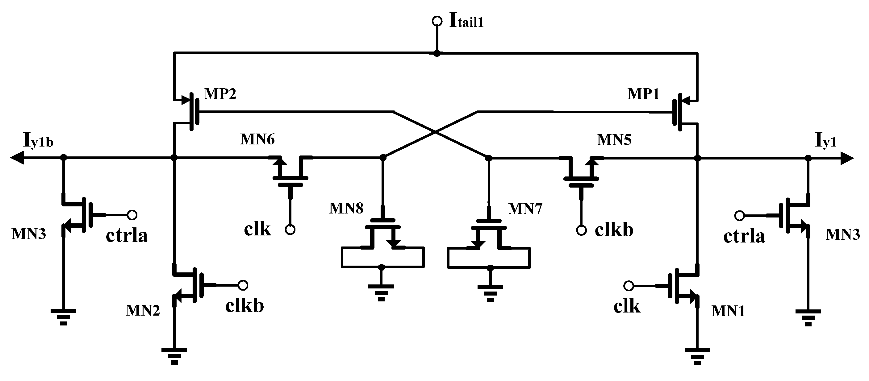
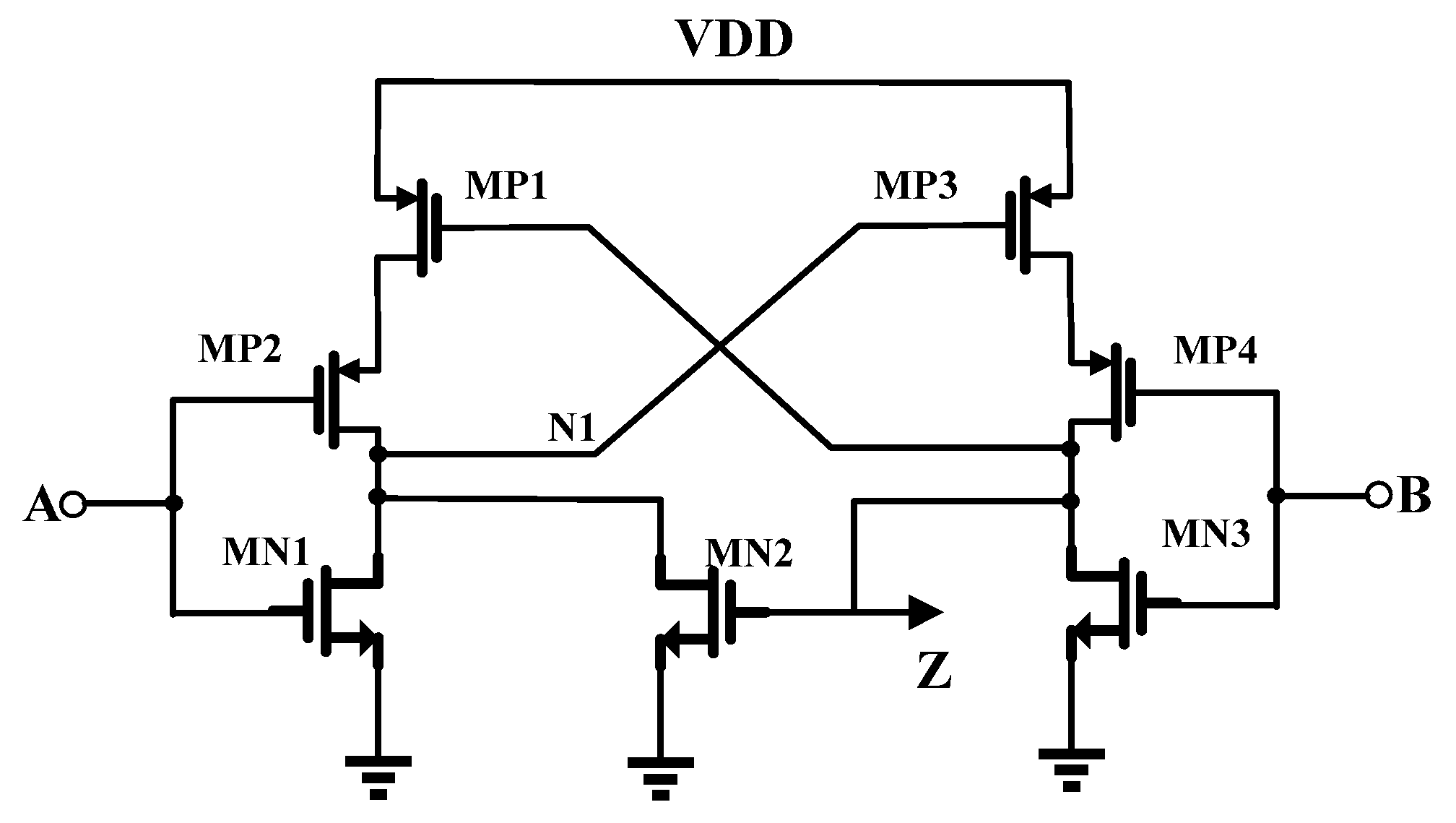
2. Circuit Design
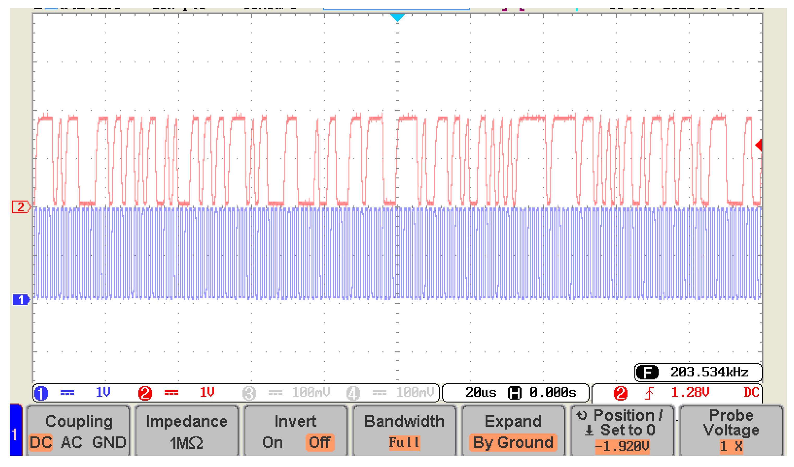
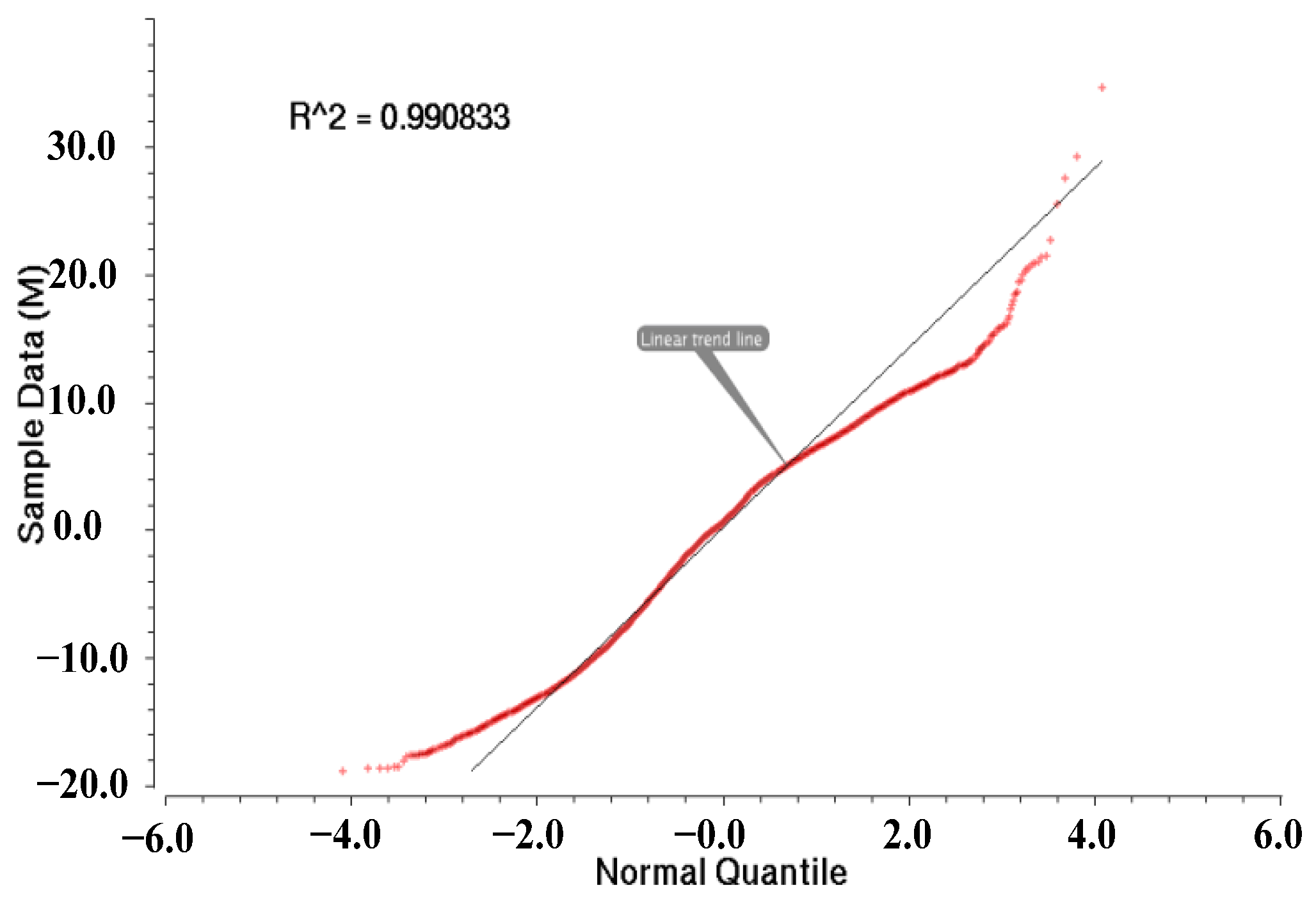
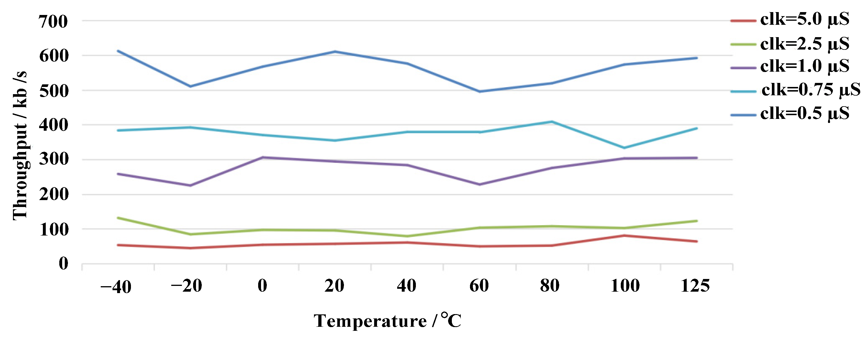
3. Measurement Results
4. Conclusions
Author Contributions
Funding
Data Availability Statement
Conflicts of Interest
References
- Huang, C.-Y.; Shen, W.C.; Tseng, Y.-H.; King, Y.-C.; Lin, C.-J. A Contact-Resistive Random-Access-Memory-Based True Random Number Generator. IEEE Electron Device Lett. 2012, 33, 1108–1110. [Google Scholar] [CrossRef]
- Balatti, S.; Ambrogio, S.; Wang, Z.; Ielmini, D. True Random Number Generation by Variability of Resistive Switching in Oxide-Based Devices. IEEE J. Emerg. Sel. Top. Circuits Syst. 2015, 5, 214–221. [Google Scholar] [CrossRef]
- Yang, J.; Lin, Y.; Fu, Y.; Xue, X.; Chen, B.-A. A small area and low power true random number generator using write speed variation of oxidebased RRAM for IoT security application. In Proceedings of the 2017 IEEE International Symposium on Circuits and Systems (ISCAS), Baltimore, MD, USA, 28–31 May 2017; pp. 1–4. [Google Scholar]
- Kim, J.; Nili, H.; Truong, N.D.; Ahmed, T.; Yang, J.; Jeong, D.; Sriram, S.; Ranasinghe, D.; Ippolito, S.; Chun, H. Nano-Intrinsic True Random Number Generation: A Device to Data Study. IEEE Trans. Circuits Syst. I Regul. Pap. 2019, 66, 2615–2626. [Google Scholar] [CrossRef]
- Chen, W.; Che, W.; Bi, Z.; Wang, J.; Yan, N.; Tan, X.; Wang, J.; Min, H.; Tan, J. A 1.04 μW truly random number generator for Gen2 RFID tag. In Proceedings of the 2009 IEEE Asian Solid-State Circuits Conference, Taipei, Taiwan, 16–18 November 2009. [Google Scholar]
- Liu, D.-S.; Liu, Z.; Li, L.; Zou, X.-C. A Low-Cost Low-Power Ring Oscillator-based Truly Random Number Generator for Encryption on Smart Cards. IEEE Trans. Circuits Syst. II Express Briefs 2016, 63, 608–612. [Google Scholar] [CrossRef]
- Wieczorek, P.-Z. Lightweight TRNG based on multiphase timing of bistables. IEEE Trans. Circuits Syst. I Regul. Pap. 2016, 63, 1043–1054. [Google Scholar] [CrossRef]
- Govindaraj, R.; Ghosh, S.; Katkoori, S. CSRO-Based Reconfigurable True Random Number Generator Using RRAM. IEEE Trans. Very Large Scale Integr. VLSI Syst. 2018, 26, 2661–2670. [Google Scholar] [CrossRef]
- Postel, P.-J.; Bazzi, H.; Aziza, H.; Canet, P.; Harb, Z. True random number generation exploiting SET voltage variability in resistive RAM memory arrays. In Proceedings of the 2019 19th Non-Volatile Memory Technology Symposium (NVMTS), Durham, NC, USA, 28–30 October 2019; pp. 1–5. [Google Scholar]
- Aziza, H.; Postel-Pellerin, J.; Bazzi, H.; Canet, P.; Moreau, M.; Della Marca, V.; Harb, A. True Random Number Generator Integration in a Resistive RAM Memory Array Using Input Current Limitation. IEEE Trans. Nanotechnol. 2020, 19, 214–222. [Google Scholar] [CrossRef]
- Nakura, T.; Ikeda, M.; Asada, K. Ring Oscillator Based Random Number Generator Utilizing Wake-up Time Uncertainty. In Proceedings of the Solid-State Circuits Conference, San Francisco, CA, USA, 8–12 February 2009; pp. 1–4. [Google Scholar]
- Amaki, T.; Hashimoto, M.; Onoye, T. An oscillator based true random number generator with jitter amplifier. In Proceedings of the International Symposium on Circuits and Systems (ISCAS), Rio de Janeiro, Brazil, 15–18 May 2011; pp. 1–4. [Google Scholar]
- Dai, L.; Harjani, R. Design of low phase noise CMOS ring oscillators. IEEE Trans. Circuits Syst. II Analog Digit. Signal Process. 2002, 49, 328–338. [Google Scholar]
- Stewart, R.; Leung, B.; Gong, G. Truly Random Number Generator Based on Ring oscillator Utilizing Last Passage Time. IEEE Trans. Circuits Syst. II Express Briefs 2014, 61, 937–941. [Google Scholar]
- Yang, K.; Fick, D.; Henry, M.-B.; Lee, Y.; Sylvester, D. A 23 Mb/s 23 pJ/b fully synthesized true-random-number generator in 28 nm and 65 nm CMOS. IEEE Int. Solid-State Circuits Conf. 2014, 16, 280–283. [Google Scholar]
- Bejar, E.; Saldana, J.; Raygada, E.; Silva, C. On the Jitter-to-Fast-Clock-Period Ratio in Oscillator-Based True Random Number Generators. In Proceedings of the 24th IEEE International Conference on Electronics, Circuits and Systems (ICECS), Batumi, Georgia, 5–8 December 2017; pp. 1–4. [Google Scholar]
- Kim, M.; Ha, U.; Lee, Y.; Lee, K.; Yoo, H.-J. A 82-nW chaotic map true random number generator based on a subranging SAR ADC. IEEE J. Solid State Circuits 2017, 52, 1953–1965. [Google Scholar] [CrossRef]
- Yang, K.; Blaauw, D.; Sylvester, D. An all-digital edge racing true random number generator robust against PVT variations. IEEE J. Solid State Circuits 2016, 51, 1022–1031. [Google Scholar]


| NIST Test | p_Value | Result |
|---|---|---|
| Frequency | 0.9850 | pass |
| Block Frequency | 0.9496 | pass |
| Cumulative Sums | 0.9114 | pass |
| Runs | 0.5341 | pass |
| Longest Run | 0.3504 | pass |
| Rank | 0.2133 | pass |
| FFT | 0.3504 | pass |
| Non-Overlapping Template | 0.7399 | pass |
| Overlapping Template | 0.3504 | pass |
| Universal | 0.5341 | pass |
| Approximate Entropy | 0.7399 | pass |
| Random Excursions | 0.1223 | pass |
| Random Excursions Variant | 0.3504 | pass |
| Serial | 0.7391 | pass |
| Linear Complexity | 0.7399 | pass |
Disclaimer/Publisher’s Note: The statements, opinions and data contained in all publications are solely those of the individual author(s) and contributor(s) and not of MDPI and/or the editor(s). MDPI and/or the editor(s) disclaim responsibility for any injury to people or property resulting from any ideas, methods, instructions or products referred to in the content. |
© 2023 by the authors. Licensee MDPI, Basel, Switzerland. This article is an open access article distributed under the terms and conditions of the Creative Commons Attribution (CC BY) license (https://creativecommons.org/licenses/by/4.0/).
Share and Cite
Chen, C.; Li, S.; Song, C. A 200 kb/s 36 µw True Random Number Generator Based on Dual Oscillators for IOT Security Application. Electronics 2023, 12, 2332. https://doi.org/10.3390/electronics12102332
Chen C, Li S, Song C. A 200 kb/s 36 µw True Random Number Generator Based on Dual Oscillators for IOT Security Application. Electronics. 2023; 12(10):2332. https://doi.org/10.3390/electronics12102332
Chicago/Turabian StyleChen, Chengying, Shuhui Li, and Changkun Song. 2023. "A 200 kb/s 36 µw True Random Number Generator Based on Dual Oscillators for IOT Security Application" Electronics 12, no. 10: 2332. https://doi.org/10.3390/electronics12102332