Article

Design of Self-Calibration Comparator for 12-Bit SAR ADCs

1
School of Physics and Electronic Sciences, Changsha University of Science and Technology, Changsha 410114, China
2
Hunan Pin Teng Technology Co., Ltd., Changsha 410006, China
3
School of Physics and Electronics, Hunan University, Changsha 410082, China
*
Author to whom correspondence should be addressed.
Electronics 2023, 12(10), 2277; https://doi.org/10.3390/electronics12102277
Submission received: 22 April 2023 / Revised: 13 May 2023 / Accepted: 15 May 2023 / Published: 18 May 2023
(This article belongs to the Special Issue Design of Mixed Analog/Digital Circuits, Volume 2)

Abstract

:
A novel self-calibration comparator for a 12-bit 2.5 MSPS successive approximation register analog-to-digital converter (SAR ADC) applied in a touch microcontroller unit (MCU) with small area, high precision, fast response speed, and low-voltage detection is proposed in this paper. A combination of input/output offset storage (IOS/OOS) and an offset trimming circuit was employed to reduce the offset of the cascade preamplifier and the operational transconductance amplifier (OTA), a novel offset trimming circuit with a 5-bit digital controller was designed to further reduce the residual offset voltage, and an improved self-calibration technology was also implemented to compensate the conversion error in SAR ADC system to a minimum. Simulation and measured results show that the input-referred offset calibrating range is ±9.15 mV at 0.61 mV/step, the low-voltage detection of SAR ADC is realized by compensating the conversion error to a minimum, and the effective number of bits (ENOB) and figure of merit (FoM) at 5 V supply and 2.5 M/s rate in the 12-bit SAR ADC with a 95 nm CMOS are 11.33 bits and 726.6 fJ/conversion-step, respectively. The proposed self-calibration comparator applied in the SAR ADC system can automatically eliminate the offset voltage caused by nonidealities and meet the requirements of the touch MCU.

1. Introduction

Successive approximation register analog-to-digital converters (SAR ADCs) are widely used in sensing detection, industrial control, and other fields because of their simple structure and low power consumption [1]. The comparator, as the core component of analog-to-digital conversion in SAR ADC, has a very important impact on the speed, accuracy, and power consumption of SAR ADC. Comparators can be separated into two main categories: the static topology working continuously and the dynamic topology making a decision after being initiated with a clock signal [2,3]. In recent years, dynamic comparators have been widely used because of their advantages of zero static power consumption, high speed, and rail-to-rail output. The dynamic comparator with low offset SR latch reported in [4] can work up to 100 MHz clock frequency while the average dynamic power and standard deviation in offset voltage are 18 µW and 3.06 mV, respectively. In [5], a dynamic latch comparator with fast response and low kickback noise was designed in a 10-bit synchronous SAR ADC; the metastable state was avoided by the effectively increased headroom for comparator to reduce the data bit error rate (BER). In [6], a regenerative feedback dynamic latch comparator was presented in a microdevice composed of a 4 × 4 array of photodiodes and readout circuits. The two cross-coupled pairs of the latch were switched through their drains to eliminate backgating effects and promote faster regeneration. The dynamic proximity comparator designed in [7] utilized latches with positive feedback at the second stage to generate rail-to-rail digital outputs. In comparison, a static comparator has high precision and low offset voltage, but it has high power consumption and low speed. A dynamic comparator has low power consumption and high speed, but its offset voltage and noise performance are relatively poor. In both the static and dynamic comparators, there are some nonidealities such as device mismatch and noise. These nonidealities will cause the offset voltage of the comparator, which will lead to decreased accuracy of the comparator. To improve the accuracy of comparators, offset cancellation techniques are usually adopted.
The conventional offset calibration techniques for comparators mainly include correlated double sampling (CDS), autozeroing, and chopper stabilization techniques [8,9]. In order to improve the speed of a comparator while ensuring accuracy, a multi-stage cascade structure is often adopted in the comparator. The most common offset cancellation techniques in these multi-stage comparators are based on using preamplifiers with input/output offset storage (IOS/OOS) techniques [10]. The two offset cancellation methods, the IOS technique and the OOS technique, were covered in [11], and they have their own merits and faults. The IOS technique stores the offset voltage on the input coupling capacitor, which has the advantage that the output of the preamplifier will not be saturated and will avoid nonlinear distortion. However, the offset voltage of the preamplifier cannot be completely canceled, and the remaining offset voltage is Vos/(A + 1) [12]. The OOS technique stores the offset voltage on the output coupling capacitor, which has the advantage that the offset voltage of the preamplifier can be eliminated completely, but the voltage gain of the single stage should not be too high to avoid nonlinear distortion. In the current comparator research, many different offset cancellation techniques based on the IOS and OOS techniques have been proposed for different applications. In [13], a four-stage static comparator combining the OOS and the CDS techniques was used to eliminate the offset caused by the input level and was applied in a two-step single-slope (SS) ADC for CMOS image sensors with a high frame rate. The dynamic latched comparator proposed in [14] adopted the IOS technique to increase the conversion linearity and was applied in a pipelined sub-ranging SAR ADC. In [15], IOS technology and neutralization technology were adopted in a quantizer that consisted of 15 comparators and applied in a sigma-delta ADC dedicated to automotive control systems to reduce the offset voltage and kickback noise, respectively. A new multi-stage preamplifier reported in [16] was based on a cascade of modified IOS amplifiers and an OOS amplifier in pipeline arrangement to effectively improve the conversion speed of the comparator and provide rail-to-rail input common-mode range (ICMR). Compared with the OOS technique, which is preferable for very high-speed comparators, the IOS technique is preferable for high-resolution comparator applications [17].
In recent years, a series of offset trimming circuits have been proposed to suppress the offset voltage with other performance guaranteed since conventional offset calibration techniques degrade the performance of the comparators due to the adjustment of the load capacitors with a set of trimming capacitors [18] or employing an extra trimming DAC [19]. An improved two-stage dynamic comparator reported in [20] used a bulk voltage trimming technique to achieve offset self-calibration. The input-referred offset calibration range was effectively improved by using the two-stage calibration. In [21], a weight biasing calibration technique was conducted during ADC startup to be suitable for biomedical implant systems. The offset calibration method proposed in [22] compensates the input-referred offset voltage by trimming the effective transconductance of the second-stage PMOS input pairs, while the degradation of the speed, noise, and power efficiency caused by the calibration circuits is less than 0.72%. A new offset trimmable comparator and a speed-up technique were presented in [23]. The body terminal of PMOS transistors was utilized as an input terminal to achieve rail-to-rail input range and meet the requirement of low-voltage applications.
Although recent publications and applications for comparators applied in SAR ADCs mainly focus on the dynamic topology, a static self-calibration comparator was designed in this study and applied in a 12-bit single-ended SAR ADC, as comparators for SAR ADCs with small area, high precision, fast response speed, high stability, and low-voltage detection are needed in touch MCU applications. The 12-bit single-ended SAR ADC targets static features such as integral nonlinearity (INL) and differential nonlinearity (DNL) and is integrated into a touch MCU chip. A combination of the OOS and IOS techniques is adopted in the seven-stage preamplifiers to improve the precision of the proposed comparator and the resolution of the 12-bit SAR ADC. A novel offset trimming calibration method with simplified control logic is proposed to further reduce the residual offset voltage of the proposed comparator. The effective transconductance of the differential input pair in the first-stage preamplifier is changed by trimming the equivalent transistor size with the equivalent MOS switches that are only added on fixed voltage nodes for offset trimming. The switched node voltages stay almost constant during the comparator operation to minimize performance degradation. A 5-bit digital calibration logic circuit deciding the offset variation was designed to improve the offset calibration range and precision. Compared with the traditional offset trimming circuit with an error register or manual calibration for the SAR ADC applied in the touch MCU, the calibration logic circuit of the self-calibration comparator proposed in this paper can automatically complete the offset calibration, and the calibration result does not need to be stored in the register during normal operation. At the same time, the low-voltage detection with the self-calibration technology of the proposed comparator is effectively realized by compensating the SAR ADC conversion errors caused by nonidealities such as line resistance in the SAR ADC system. As a result, the chip implementation and measurement results demonstrate that the 12-bit SAR ADC conversion error caused by the line resistor can be calibrated effectively based on the proposed self-calibration comparator.
This paper is organized as follows: Section 2 introduces the design of the comparator circuit, the offset cancellation technology, and the proposed offset trimming circuit. Section 3 presents the simulation and analysis of the proposed comparator. Section 4 explains the principle of the self-calibration comparator applied in a 12-bit SAR ADC system and shows the chip implementation and measurement results. Section 5 finally presents the conclusion.

2. Design of Comparator Circuit

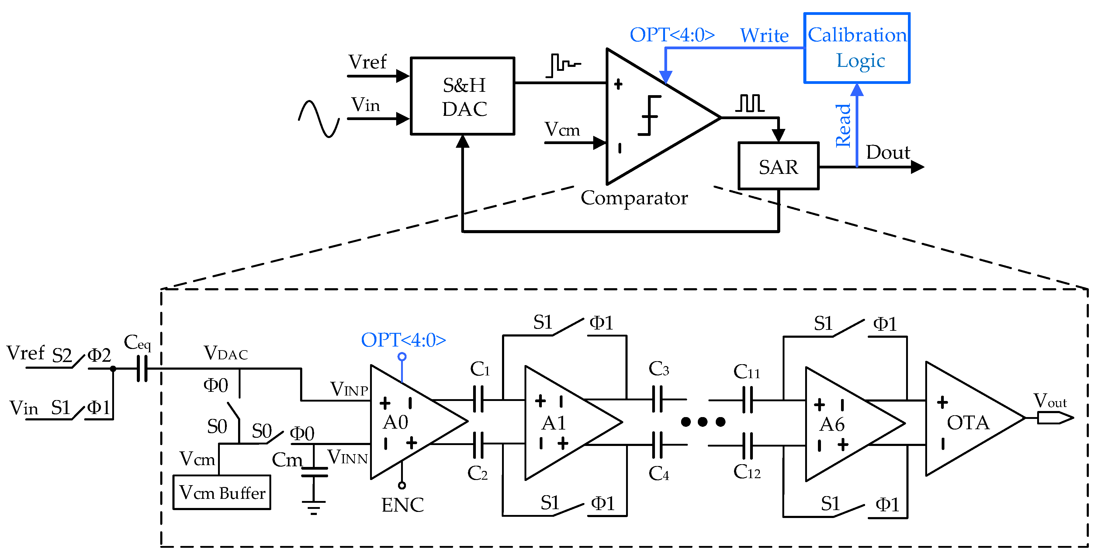
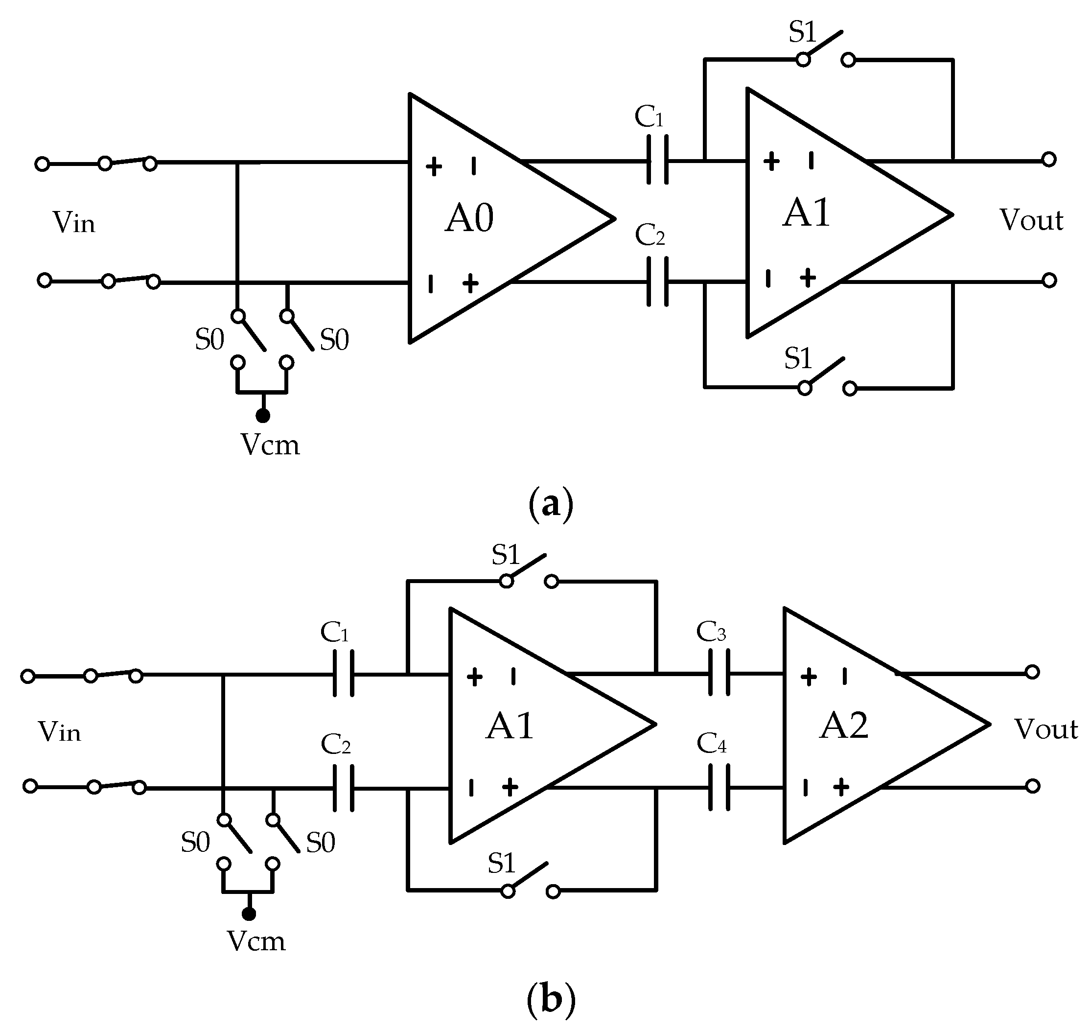
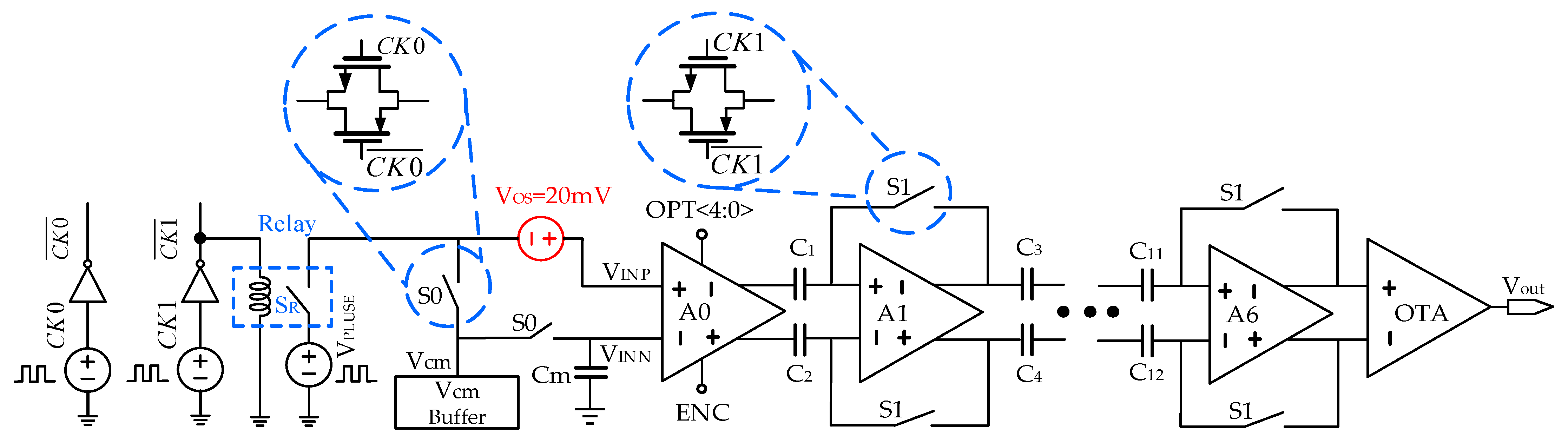
2.1. Overall Circuit Structure of Comparator

A conventional SAR ADC consists of a comparator, a digital-to-analog converter (DAC), and successive approximation register (SAR) control logic. Since the offset voltage of the comparator is one of the main factors that limit the accuracy of SAR ADCs, a self-calibration technique based on the structure of a conventional SAR ADC is proposed in this paper to eliminate the offset voltage of the comparator automatically. Under the control of a calibration logic circuit based on self-calibration technology, the conversion error caused by nonidealities such as line resistors could be compensated to a minimum. Figure 1 shows the structure of the proposed self-calibration comparator applied in a 12-bit SAR ADC system, which consists of a common-mode buffer (Vcm Buffer), seven-stage preamplifiers (A0 to A6), and an open-loop operational transconductance amplifier (OTA). The preamplifiers A0 to A6 are used to increase the speed of the comparator, while the first stage A0 is mainly used for small signal amplification. In order to improve the unit gain bandwidth (GBW) of the multi-stage amplifiers to increase their speed, the first stage A0 was designed with a wide bandwidth, and the last stage OTA was designed with a large swing rate.
OPT<4:0> is a digital controller represented by a 5-bit binary code, and it is connected to the offset trimming circuit inside the first-stage preamplifier (A0). The offset voltage of the proposed comparator can be adjusted by using OPT<4:0>. The proposed comparator operates in two clock phases: the sampling phase and the comparison phase. During the sampling-phase period, switches S1 and S0 turn on, and Φ1 and Φ0 are high, while switch S2 turns off and Φ2 is low. The Vcm Buffer is connected to the VINN of the first-stage amplifier A0 of the proposed comparator to provide the common-mode voltage Vcm. During the sampling-phase period, the Vcm Buffer charges the holding capacitor Cm. The equivalent capacitor (Ceq) of the DAC capacitor array is connected to the VINP of the first-stage amplifier A0 of the proposed comparator, and the analog signal is sampled on the equivalent capacitor Ceq. The proposed comparator serves as the sample-and-hold (S&H) function and will sample the analog input (Vin). During the comparison-phase period, switches S1 and S0 turn off, and Φ1 and Φ0 are low, while switch S2 turns on and Φ2 is high. The proposed comparator compares the input signals, the VINN and VINP, and provides the binary output (Vout).
Typically, the error caused by the comparator during ADC conversion is less than 0.5 LSB, and the output swing is required to be at least 0.5 VDD. Therefore, the minimum voltage gain Av0(min) required by the proposed comparator in Figure 1 is calculated in Equation (1):
A v 0 ( min ) = 0.5 V D D 0.5 · V r e f / 2 N = 1 × 2 12 72.2   dB
where N = 12 is the resolution of the SAR ADC for the comparator proposed in this paper; Vref = 5 V and VDD = 5 V are the reference voltage and power supply, respectively. As can be determined from Equation (1), the voltage gain of the proposed comparator cannot be lower than 72.2 dB.

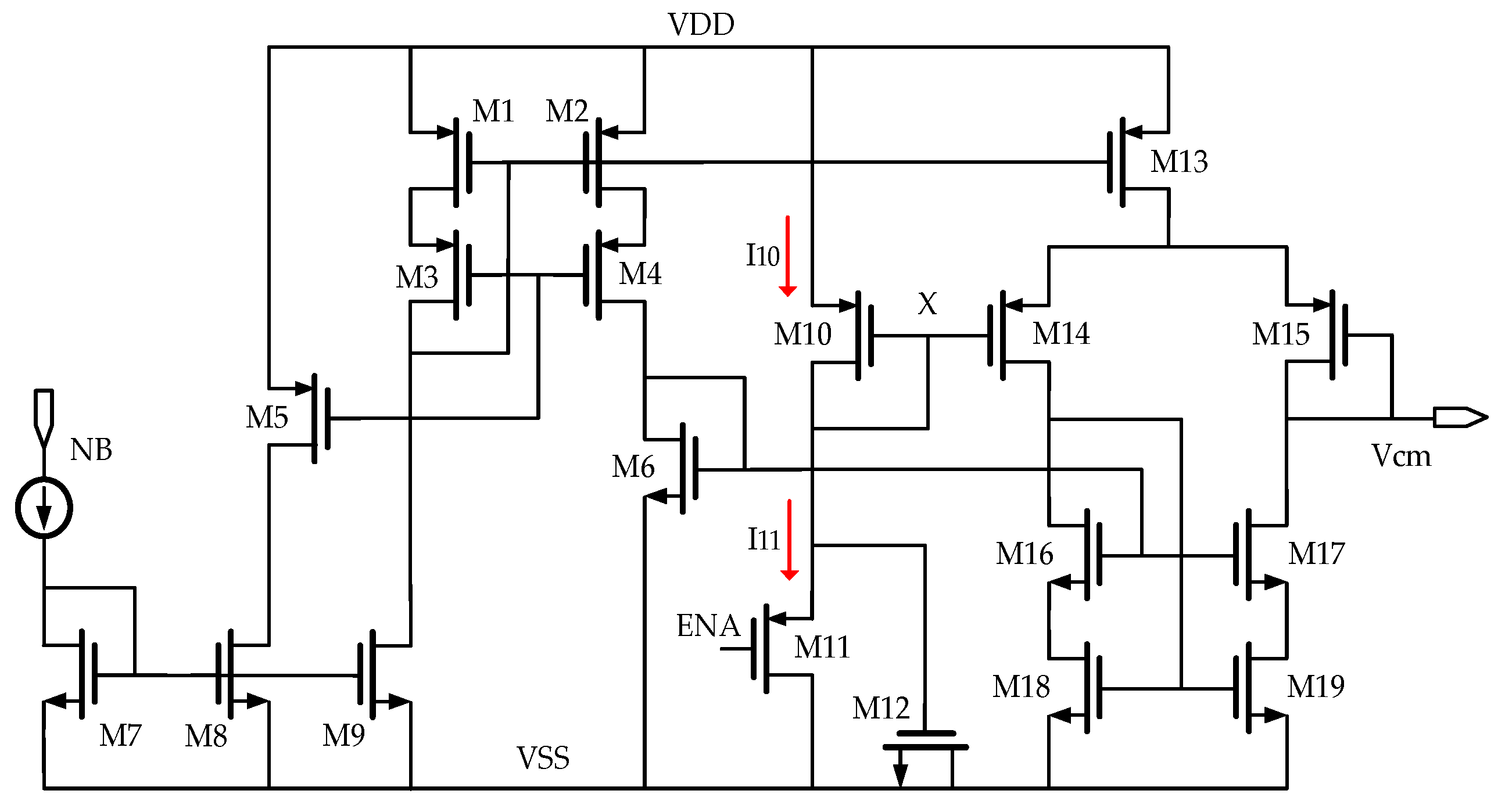
2.2. Design of the Common-Mode Buffer

The stability of the common-mode signal (Vcm) directly affects the accuracy of the final output of the proposed comparator. As shown in Figure 2, the gate and drain of M10 are tied together to form an MOS diode. An active-resistance voltage divider consisting of M10 and M11 is adopted to form a bias voltage Vx at node X. A cascode amplifier consisting of M13 to M19 is connected as a buffer at node X to provide sufficient voltage driving capability for the bias voltage Vx.
Transistors M16 to M19 form a cascode current mirror as an active load to improve the gain of the cascode amplifier. The gate of M15 operating as negative input of the cascode amplifier is connected to the output (Vcm) to form a voltage follower. The transistor M12 is an MOS capacitor used for the establishment of Vcm. When ENA = 0, M11 operates in the saturation region, which is equivalent to an active load. As illustrated in Figure 2, the currents flowing through M10 and M11 are I10 and I11, respectively, which are expressed by Equations (2) and (3).
I 10 = 1 2 μ p C ox ( W L ) 10 ( V D D V X | V T H 10 | ) 2
I 11 = 1 2 μ p C ox ( W L ) 11 ( V X | V T H 11 | ) 2
where μ p is the carrier mobility of the PMOS devices; (W/L)10 and (W/L)11 are the transistor sizes of M10 and M11, respectively; and VTH10 and VTH11 are the threshold voltages of M10 and M11, respectively. When (W/L)10 = (W/L)11, I10 = I11, VTH10 = VTH11, and Vcm = VX, the common-mode voltage Vcm is Vcm = VDD/2 to ensure that the flip time of the proposed comparator is as short as possible if the input voltage VINP of the first-stage amplifier A0 is in the range of 0-VDD.

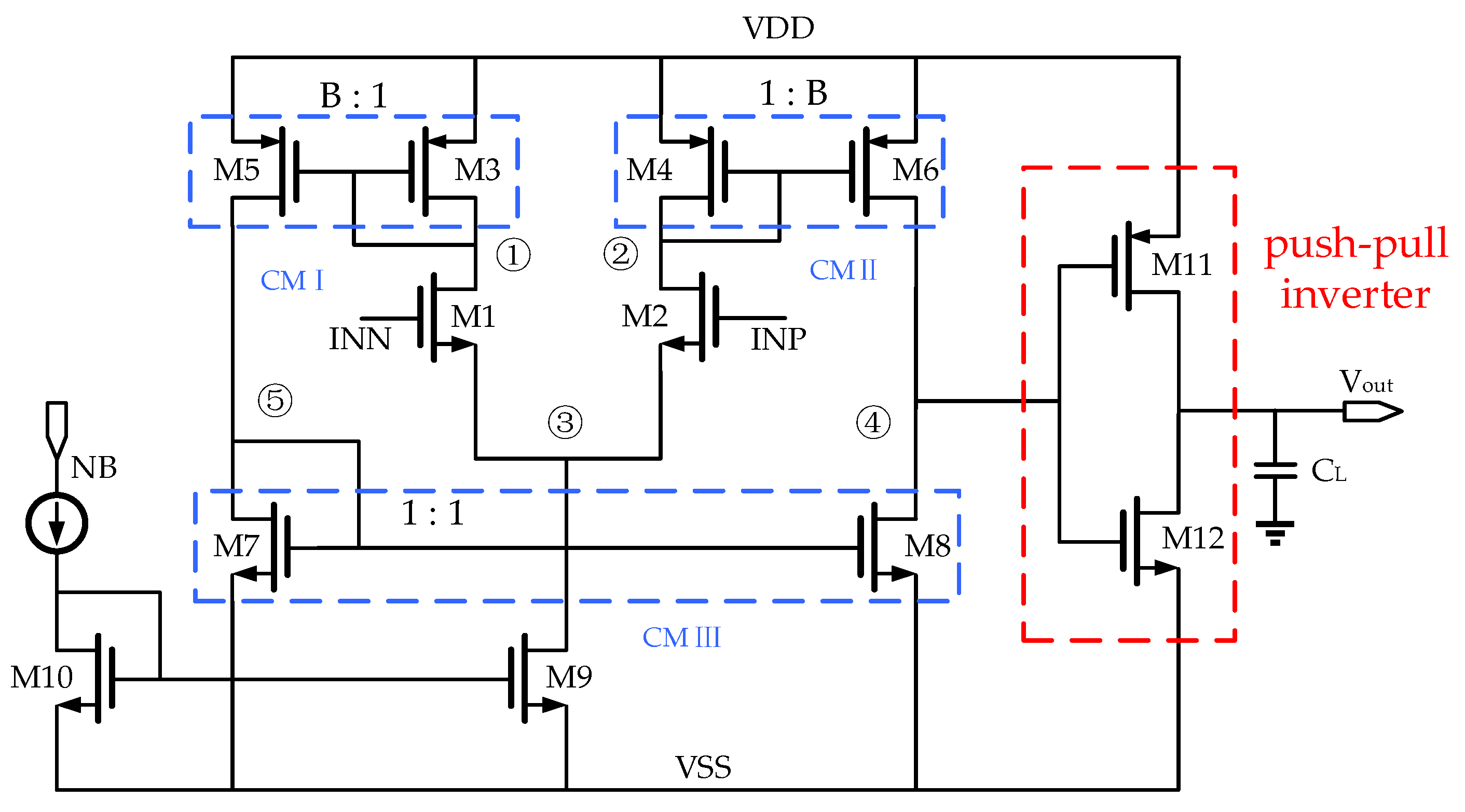
2.3. Design of the OTA

The OTA shown in Figure 3 is a symmetrical OTA that is more symmetrical than the Miller OTA and improves the matching to provide better offset and CMRR specifications [24]. The symmetrical OTA consists of one differential pair and three current mirrors (CMs), CMI, CMII, and CMIII, respectively. The differential input pair M1 and M2 is loaded with two identical current mirrors CMI and CMII providing a current gain B. A sufficient voltage gain is provided by the symmetrical OTA to allow the output voltage Vout of the proposed comparator to meet the digital signal voltage requirements of the 12-bit SAR ADC. The symmetrical OTA operates in the open-loop state, and its output at node ④ is connected to the input of a push–pull inverter to drive the push–pull inverters consisting of transistors M11 and M12. Under the condition of using the same transistors, the push–pull inverters can effectively increase the output swing.
As the output resistance at node ④ is the only high-resistance node with large gain and swing, while all the output resistances at other nodes ①, ②, ③, and ⑤ are about 1 / g m , which is low resistance, the symmetrical OTA is also a single-stage amplifier with the dominant pole at node ④. The voltage gain Av,OTA at low frequencies and the GBW of the symmetrical OTA can be easily obtained from Formulas (4) and (5), respectively.
A v , O T A = g m 1 B R n 4 = 2 V E n L 6 ( V G S V T H ) 1
G B W = B g m 1 2 π C L
where B = ( W / L ) 5 ( W / L ) 3 = ( W / L ) 6 ( W / L ) 4 is the current factor and cannot be too large as the power consumption depends on the current of each branch in the OTA. VEn is the early voltage per unit length expressed in V/μm and is constant for a certain technology. Rn4 is the output resistance at node ④, L6 is the channel length of the transistor M6, gm1 is the transconductance of the transistor M1, and CL is the load capacitor.

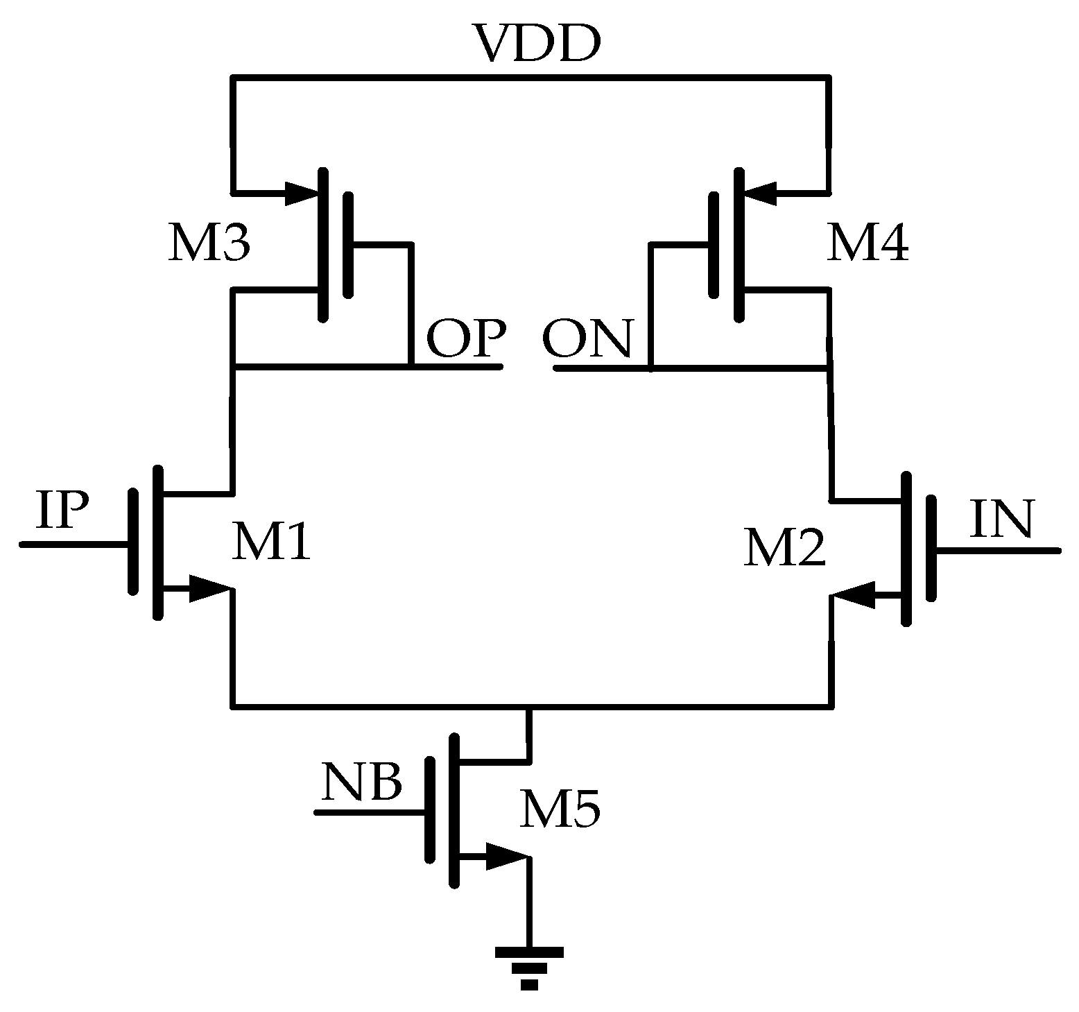
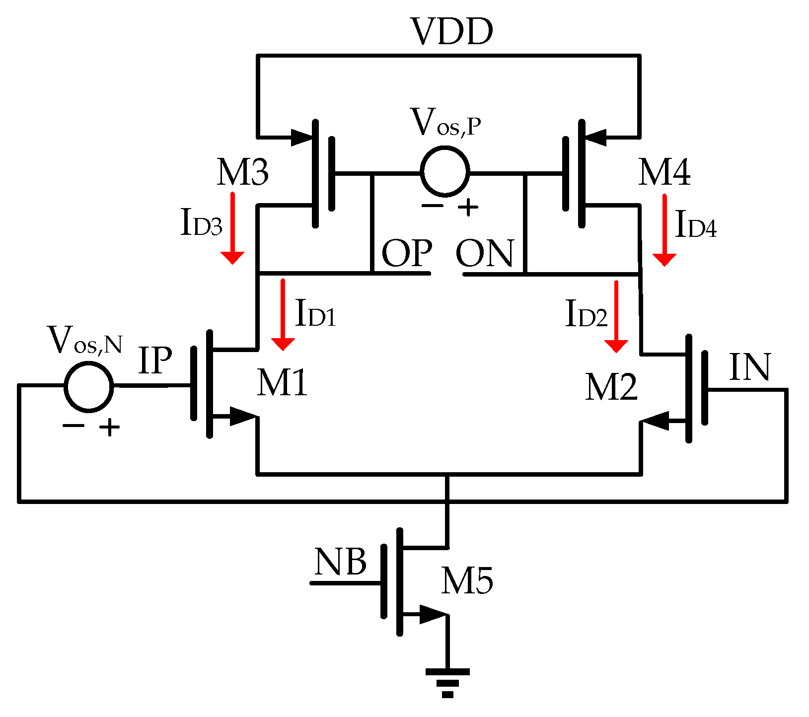
2.4. Design of the Differential Preamplifier

As the gain of each of the single-stage preamplifiers A0 to A6 is small, the multi-stage preamplifiers with cascade structure are adopted to improve the gain effectively while ensuring the bandwidth in the proposed comparator. In this study, the preamplifiers A0 to A6 use the differential amplifier structure shown in Figure 4 and determine the speed and precision of the proposed comparator. Transistors M3 and M4 are used as diode-connected loads. Transistor M5 operates in the saturation region and is equivalent to a tail current source to suppress the effect of the input common-mode level variations on the output OP and ON levels and the operation of transistors M1 and M2 [25]. As the diode-connected loads consume voltage headroom, there is a trade-off between the output voltage swings, the voltage gain, and the ICMR. The small-signal differential gain Avd can be calculated using Equation (6).
A v d = g m 1 ( g m 3 1 r O 1 r O 3 ) g m 1 g m 3
where gm1 and gm3 are the transconductances of M1 and M3, respectively. rO1 and rO3 are the resistances of M1 and M3, respectively. When gm1 and gm3 are expressed in terms of device dimensions, the Avd can be computed as shown in Equation (7):
A v d μ n ( W / L ) 1 μ p ( W / L ) 3
where μ p and μ n are the mobility of the PMOS and NMOS devices.

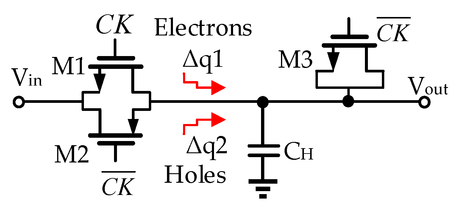
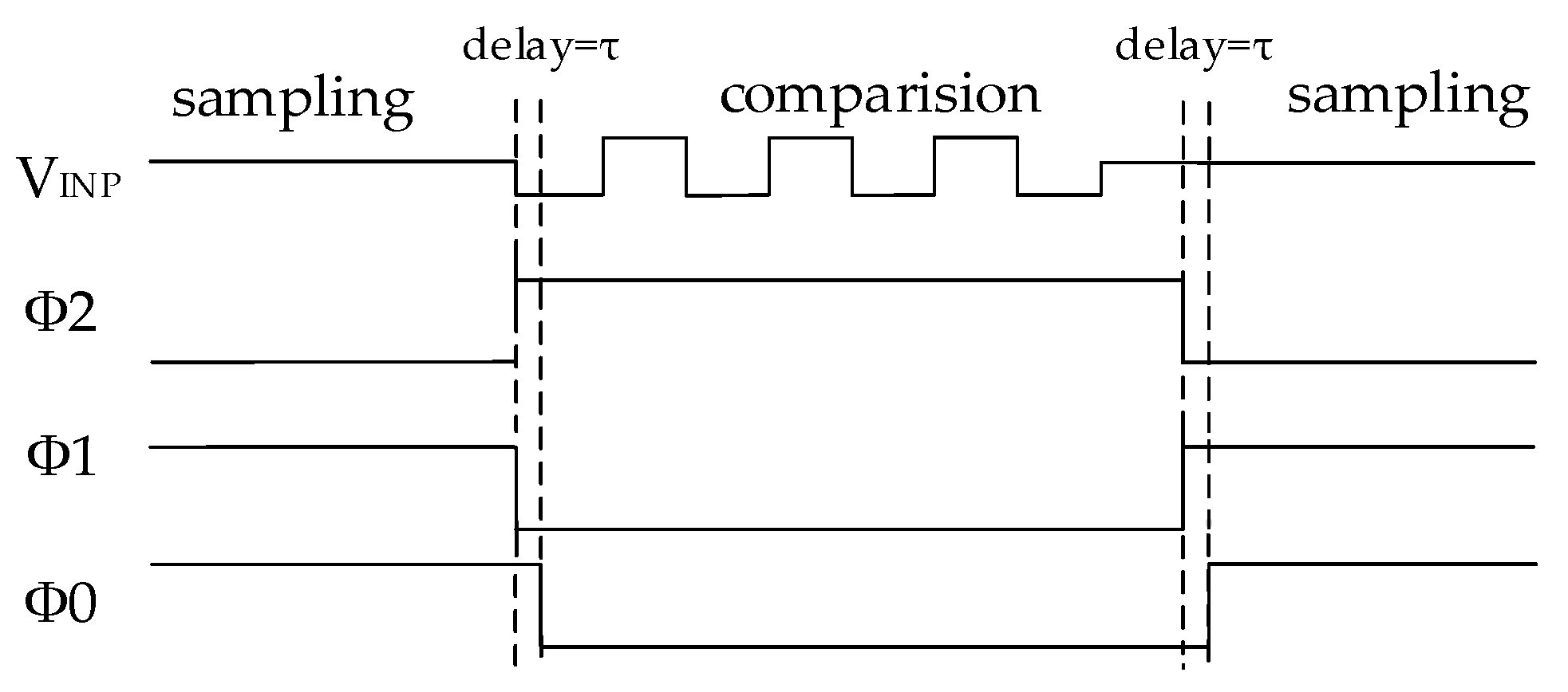
2.5. Design of the Offset Cancellation Technology

The OOS and IOS techniques are adopted in the proposed comparator to cancel the input-referred offsets of preamplifiers A0 to A6. The preamplifier A0 with the OOS and the preamplifier A1 with the IOS are shown in Figure 5a,b, respectively. The residual input–residual offset of the preamplifier A0 and the preamplifier A1 can be expressed as Formulas (8) and (9), respectively. For the later preamplifiers A2 to A6 with the IOS, the Vos is stored in the capacitors at the input of the preamplifiers A2 to A6 during the sampling-phase period, and then it is reduced during the comparison-phase period. The residual offset of the preamplifier A0 with the OOS is smaller than that of the preamplifiers A1 to A6 with the IOS. Since the offset voltage of the preamplifier A0 will be amplified by the subsequent multi-stage preamplifiers A1 to A6, the OOS cancellation applied in A0 plays a significant role in the offset reduction of the proposed comparator.
V o s , O O S = Δ Q A 1 C + V o s 2 A 1
V o s , I O S = V o s 0 1 + A 0 + Δ Q C + V o s 1 A 0
where Vos0 and A0 are the input offset and gain of the preamplifier A0, respectively. ΔQ is the mismatch in charge injection from switch S1 to capacitors C1 and C2, and Vos1 is the offset voltage of preamplifier A1. Vos2 and A1 are the input offset of the preamplifier A2 and the gain of the preamplifier A1, respectively.

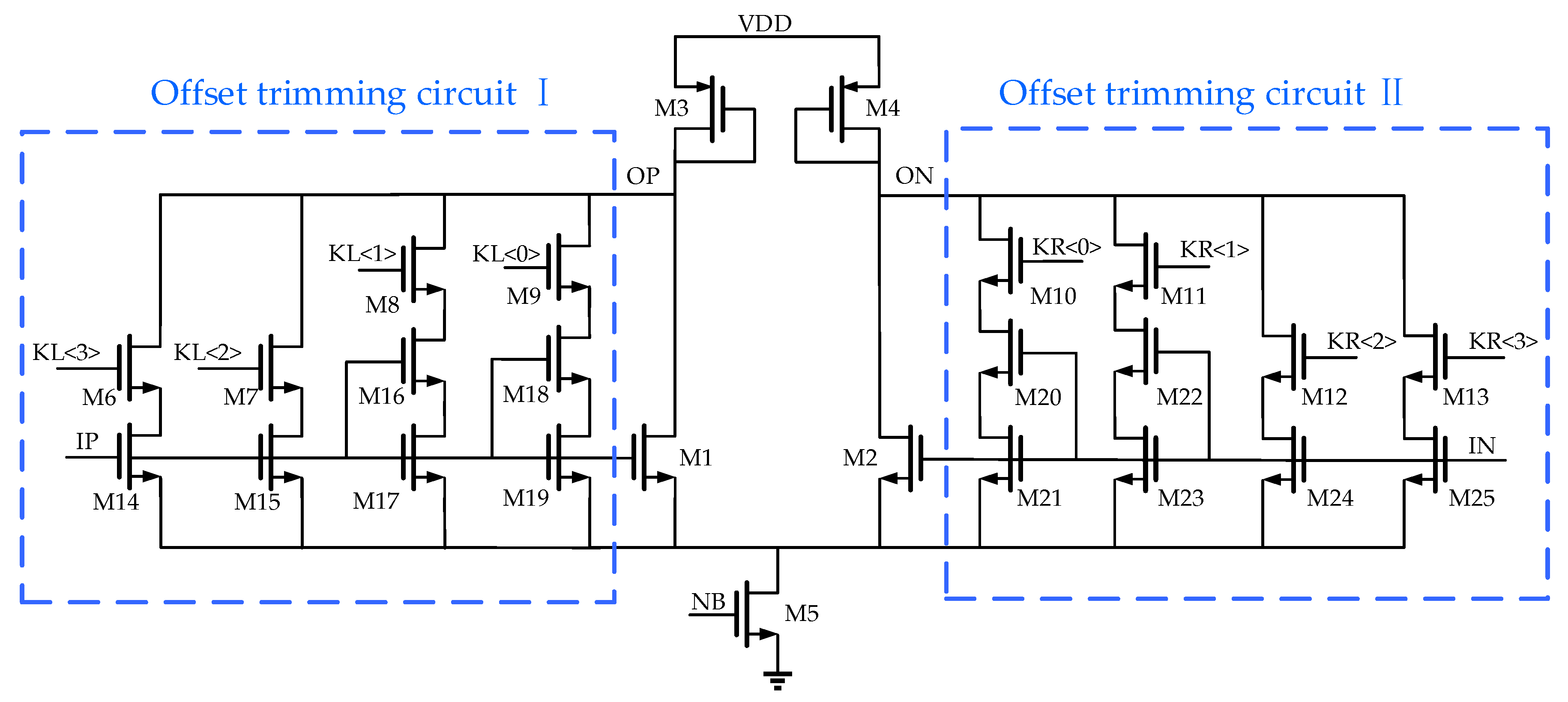
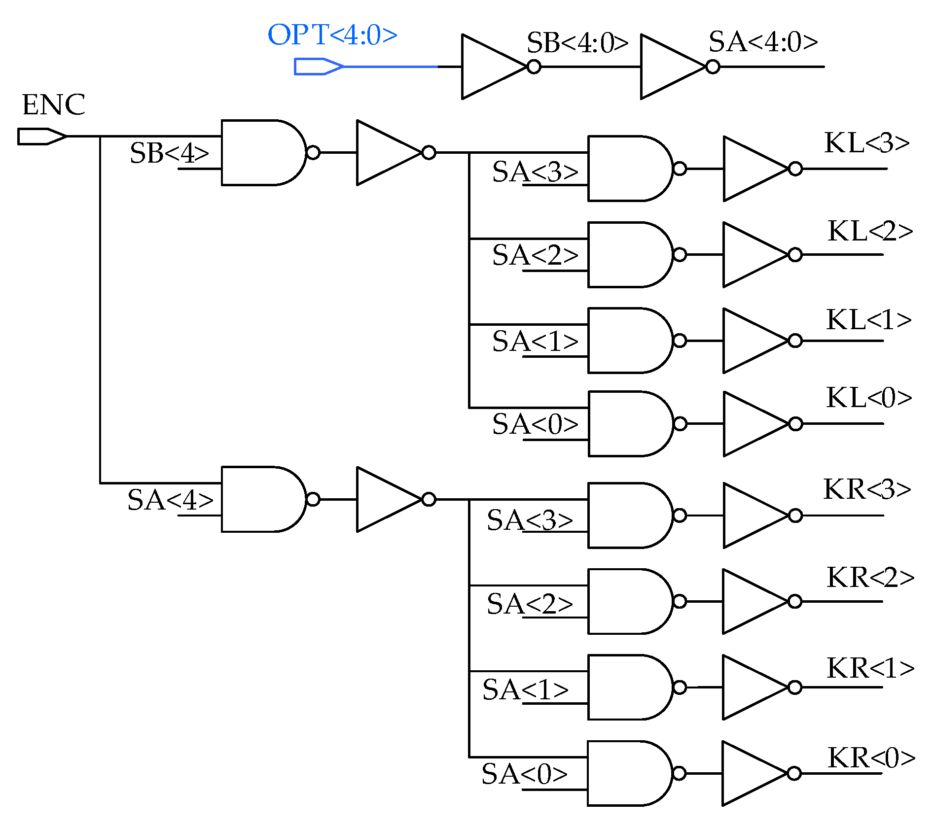
2.6. Design of the Offset Trimming Circuit
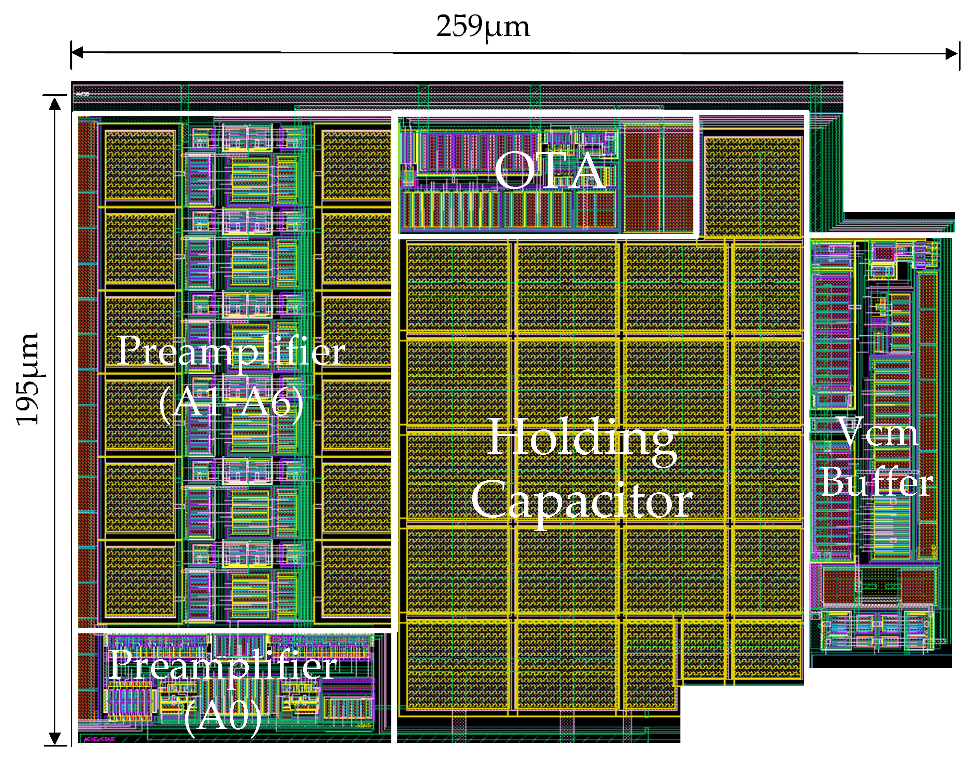
During the 12-bit SAR ADC conversion, the offset voltage of each of the single-stage preamplifiers A0 to A6 in the proposed comparator also is affected by many nonidealities such as the mismatch of transistor size, threshold voltage mismatch ΔVTH, and process parameter mismatch Δ ( μ C ox W L ) . The relationships between ΔVTH, Δ ( μ C ox W L ) and transistor size (WL) are expressed by Formulas (10) and (11), respectively [26].
Δ V T H = A V T H W L
Δ ( μ C ox W L ) = A K W L
where AVTH and AK are proportionality coefficients, which can be looked up in the process file.
As shown in Figure 6, the voltage sources V o s , N and V o s , P are the equivalent offset voltage of the single-stage preamplifiers A0 to A6 and are presented as Formulas (12) and (13), respectively. When I D 1 = I D 2 and I D 3 = I D 4 , the input offset voltage V os , in of the single-stage preamplifier is expressed as Equation (14).
V os , N = ( V G S V T H ) N 2 Δ ( W / L ) ( W / L ) N + Δ V T H , N
V os , P = | V G S V T H | P 2 Δ ( W / L ) ( W / L ) P + Δ V T H , P
V os , in = g m P g m N V os , P + V os , N
where the subscripts N and P denote NMOS and PMOS, respectively.
According to Equations (10)–(14), a novel offset trimming circuit is designed in the first-stage preamplifier A0 to effectively further suppress the offset voltage of the high-performance comparator by trimming the effective transconductance of the NMOS input pairs (M1 and M2), as shown in Figure 7. It consists of the perfectly symmetrical offset trimming circuits I and II. The differential pair transistors M1 and M2 and the offset trimming transistors M14 to M25 adopt the combination of series and parallel to solve the limitation of the resolution of the offset calibration caused by the minimum transistor size, and the adjustment precision is effectively improved. The transistors M6 to M13 are equivalent to MOS switches, realizing the series and parallel structure of the offset trimming transistors. The on and off of the equivalent MOS switches are controlled by the outputs KL<3:0> and KR<3:0> of the control logic circuit to determine the offset trimming variation. The series and parallel equivalent dimensions of the offset trimming transistors M14 to M25 can be calculated using Equations (15) and (16), respectively.
( L W ) eq = L 1 + + L N W = i = 1 N L i W
( W L ) eq = W 1 + + W N L = i = 1 N W i L
where (L/W)eq and (W/L)eq are the equivalent transistor size ratios, N is the number of transistors, and L and W are the channel length and width, respectively.
The corresponding control logic circuit of the novel offset trimming circuit is shown in Figure 8. The 5-bit digital controller OPT<4:0> is disabled until ENC = 1. During the sampling phase, when ENC = 0, all the trimming transistors M14 to M25 are not incorporated into the differential pair of the amplifier A0. During the comparison-phase period, when ENC = 1, the corresponding offset trimming transistors are incorporated into the differential input pair of the amplifier A0. The 5-bit code of digital controller OPT<4:0> is divided into two parts: high bit OPT<4> and low 4-bit OPT<3:0>. The OPT<4> bit controls whether the offset trimming circuits I and II are incorporated into the corresponding positive input (IP) or negative input (IN) of the difference pair, and the low 4-bit OPT<3:0> determine the outputs of the KL<3:0> and KR<3:0> to control the offset trimming transistors incorporated into the differential pair and change the equivalent transistor size. In order to improve the adjustment precision, the offset trimming variation needs to be as small as possible during each adjustment. The input offset voltage is calibrated by the control signal OPT<4:0> adjusting the equivalent transistor size of the offset trimming transistors incorporated into the differential pair. Based on sufficient simulation verification, the relationship between the control signal OPT<4:0> code and the corresponding offset trimming variation is shown in Table 1. When the control signal OPT<4:0> code changes one gear, the corresponding offset trimming variation is changed by only 0.5 LSB, less than 1 LSB, and the adjustment precision is effectively improved.
For the 12-bit SAR ADC and the 5 V reference voltage, the least significant bit (LSB) can be calculated using Equation (17). The maximum offset variation that can be calibrated is 7.5 LSB, which is approximately 9.15 mV.
L S B = V r e f 2 N = 5 2 12 V 1.22   mV
Whether the digital controller OPT<4:0> is enabled or not depends on the on and off state of switches S0, S1, and S2, as shown in Figure 1. The circuit of the switches with the dummy transistor M3 and a complementary switch consisting of an NMOS transistor (M1) and a PMOS transistor (M2) to reduce the effect of charge injection and cancel clock feedthrough is shown in Figure 9. A delayed clock Φ0 is designed to further remove charge injection and clock feedthrough depending on the input (Vin) between switches S1 and S0. Based on the simulation verification, the delay time between the delayed clock Φ0 and the clock Φ1 is approximately τ = 1   ns . The timing diagram of the proposed comparator offset trimming is shown in Figure 10. During the comparison-phase period, when CK = 0, the transistors M1 and M2 operate in the off region, and the switch S0 turns off with a delay of τ = 1   ns after the switch S1 turns off. The digital controller OPT<4:0> is enabled, and the equivalent MOS switches M6 to M11 in Figure 8 are turned on and control the offset trimming circuit to decide the required offset variation. During the sampling-phase period, when CK = 1, the transistors M1 and M2 operate in the saturation region, and the switch S0 turns on with a delay of τ = 1   ns after the switch S1 turns on. The digital controller OPT<4:0> is disabled, all the equivalent MOS switches are turned off, and no offset trimming transistors are connected to the input differential pair of the preamplifier A0.

2.7. Layout Design

The layout of the proposed comparator in Figure 1 is shown in Figure 11. In the layout design, the matching of circuit blocks is improved by a symmetrical arrangement of the preamplifiers A1 to A6 for the multi-stage amplifiers and the offset cancellation capacitors C1 to C12, and the influence of layout design on comparator performance is reduced. The design of a large-area voltage-holding capacitor ensures the stability of the common-mode voltage Vcm and suppresses power supply ripples. The overall layout area of the proposed comparator is 259 × 195 μm2.

3. Simulation and Analysis of the Proposed Comparator

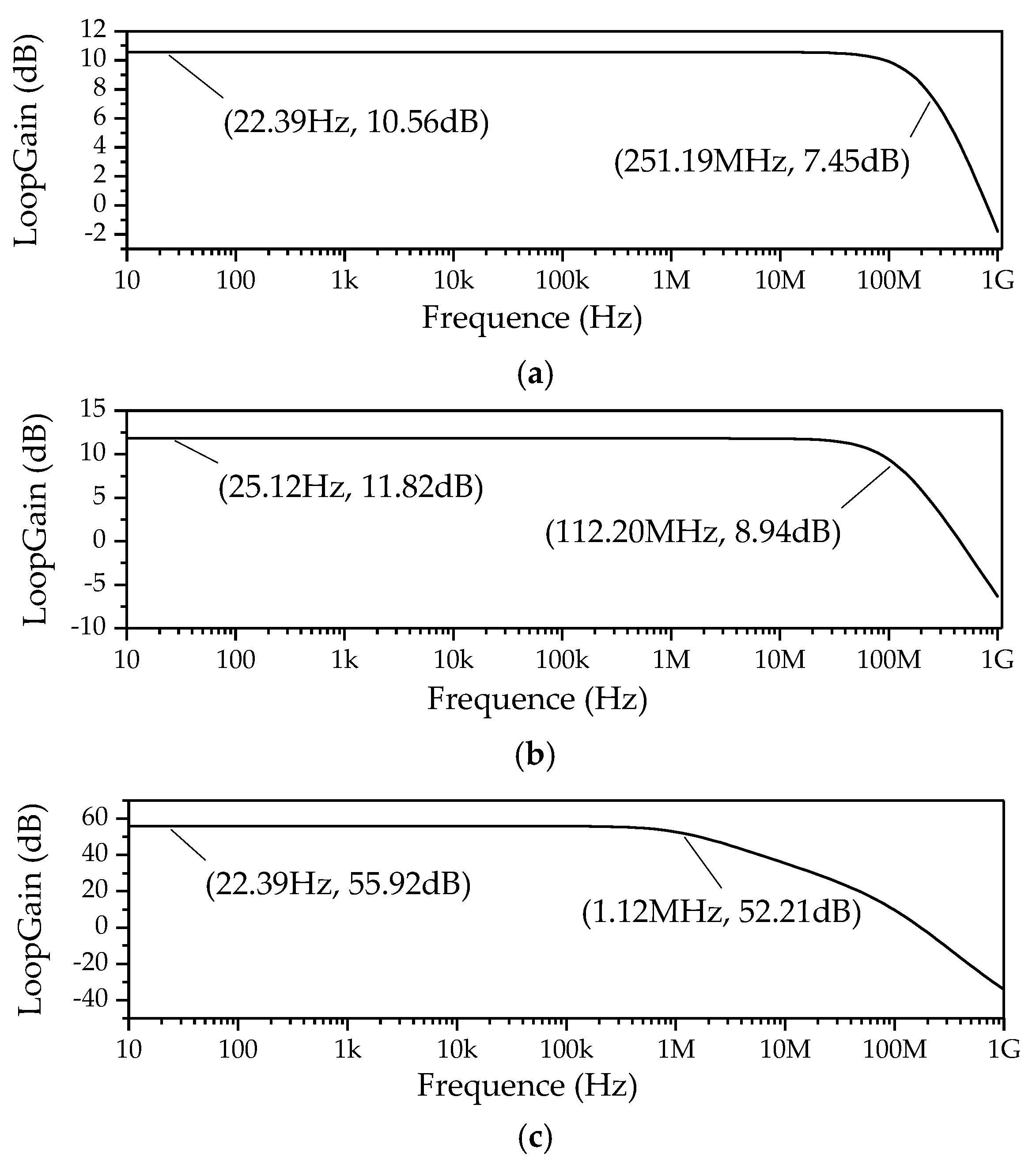
3.1. Voltage Gain and GBW of Comparator

The amplitude–frequency response curves of the preamplifier A0, the single-stage amplifier of the cascade amplifier Ai (i = 1, 2, …, 5, 6), and the OTA amplifier are shown in Figure 12a–c, respectively. The preamplifier A0 has a small signal voltage gain of 10.56 dB, and the −3 dB bandwidth is 251.19 MHz. The voltage gains and the −3 dB bandwidths of the single-stage amplifier of the cascade amplifier Ai (i = 1, 2, …, 5, 6) and the OTA amplifier are 11.82 dB and 112.20 MHz, 55.92 dB and 1.12 MHz, respectively. The voltage gain of preamplifier A0 is smaller than those of preamplifiers A1 to A6, which can ensure that the output of the preamplifier A0 will not be saturated and will avoid nonlinear distortion. The calculated total gain of the comparator is 137.4 dB, much higher than the 72.2 dB obtained from Formula (1), which can meet the design requirements.

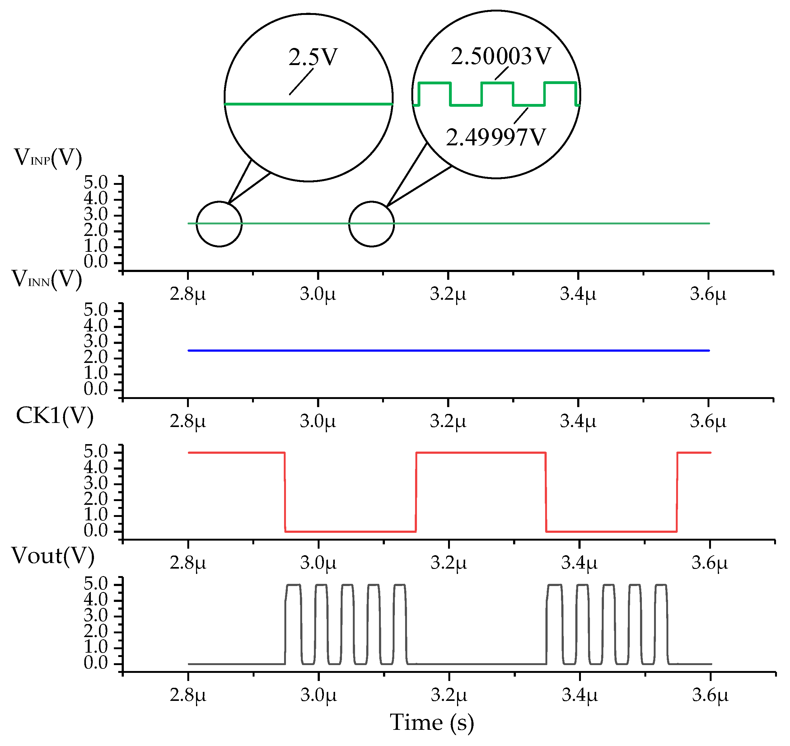
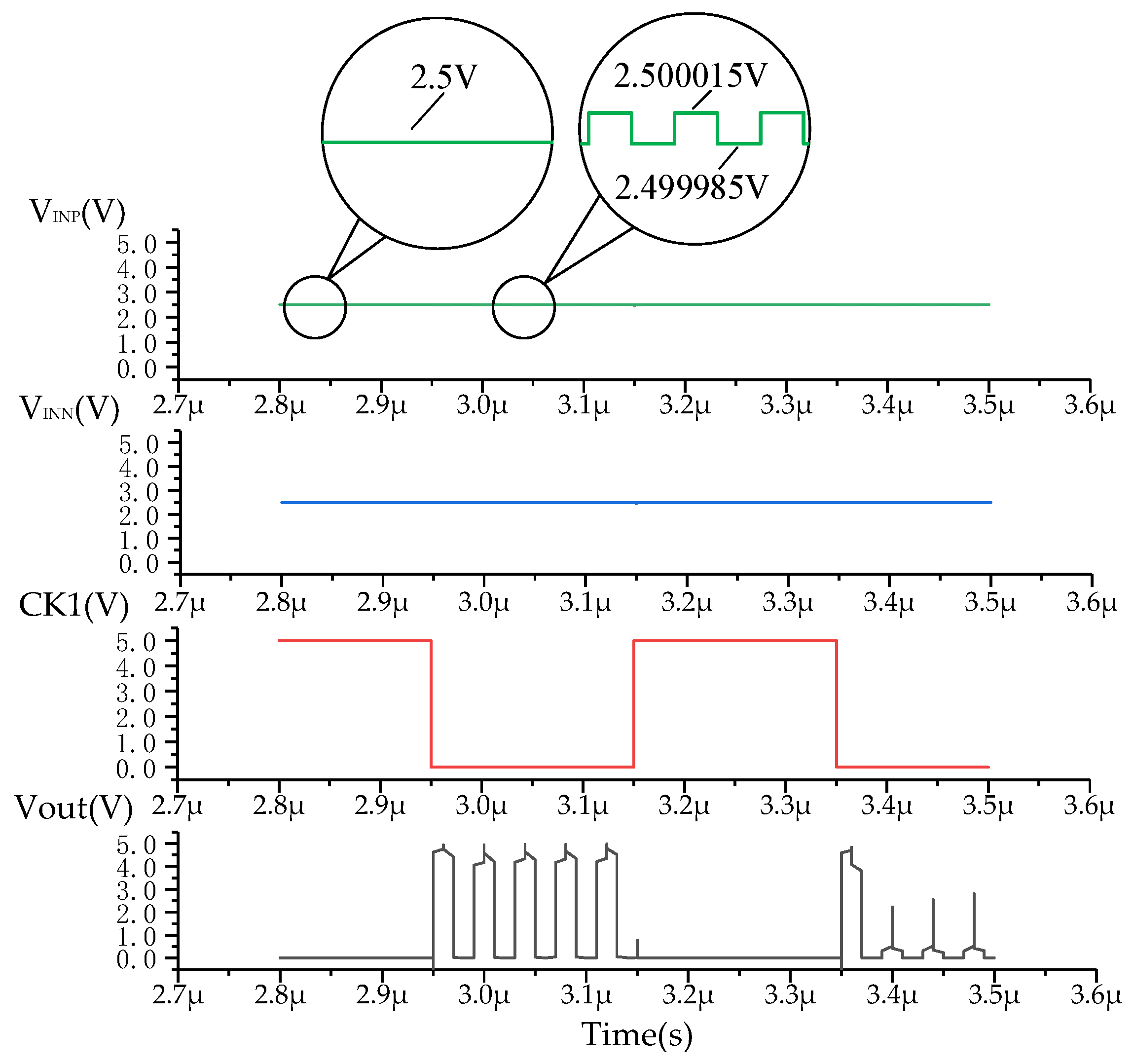
3.2. Transient Simulation of the Comparator

A typical method to simulate the speed of the comparator is the transient simulation of the comparator that assesses whether the comparator accurately turns over within the specified time to judge whether the speed of the comparator meets the requirements [27]. The transient simulation test bench of the proposed comparator is shown in Figure 13. The switches S1 and S0 are controlled by the clock signals CK1 and CK0 that is delayed by CK1 for τ = 1   ns . The voltage source VPULSE representing the signal VDAC in Figure 1 is a rectangular pulse signal; its pulse width is 20 ns, and its amplitude is 2.5 V with a 30 μV ripple. The 30 μV ripple on VPULSE is used to test the precision of the proposed comparator, and the clock frequency of the VPULSE is set at 50 MHz to test whether the comparator can meet the speed requirement of 2.5 MS/s. For simplicity, both the sampling time and the comparison time are 200 ns. As the offset voltage of the comparator is normally approximately 5 mV to 20 mV [28,29], a 20 mV DC voltage source Vos is equivalent to the DC input offset voltage and superimposed with the voltage source VPULSE to provide the input VINP for the preamplifier A0. VPULSE is under the control of a relay, and whether switch SR turns on or off depends on the logic level of the clock signal CK1.
The transient simulation results of the proposed comparator are shown in Figure 14. During the sampling-phase period, the clock signal CK1 is a logic high (VDD), SR turns off, and VINP = VINN = 2.5 V. During the comparison-phase period, the clock signal CK1 is a logic low (0), SR turns on, and VINP = VPLUSE. When VINP > VINN, the output is Vout = 1, whereas the output is Vout = 0 when VINP < VINN. The results show that the proposed comparator can correctly output high and low levels at the conversion rate of 2.5 MS/s and eliminate the influence of the input offset voltage Vos effectively. As shown in Figure 15, when the ripple on VPULSE is lower than 30 μV, the comparator is not able to correctly output high and low levels. Therefore, the precision of the proposed comparator is 30 μV.

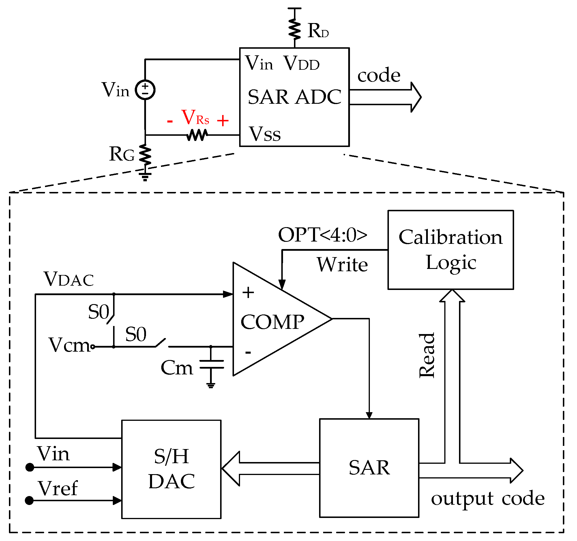
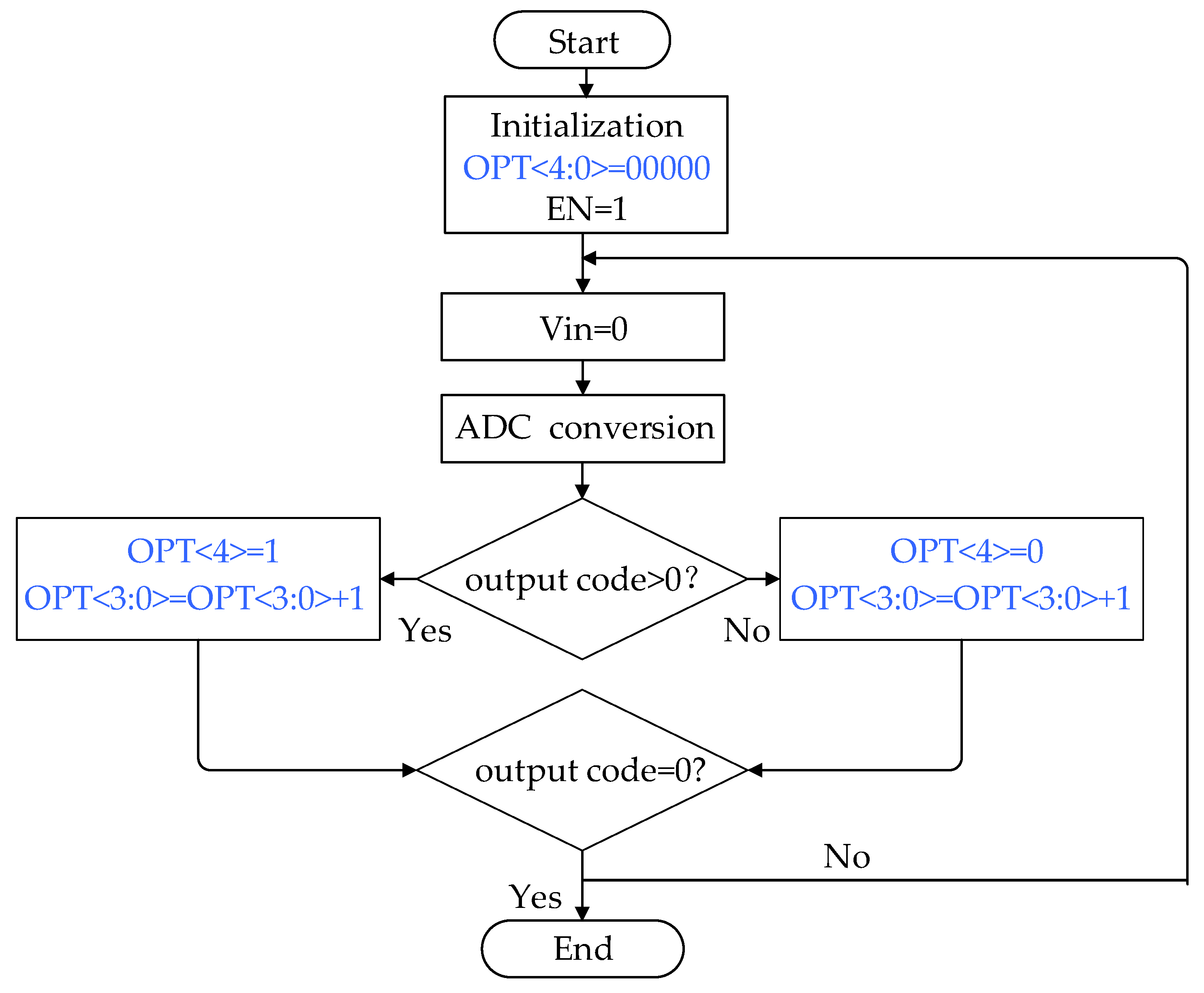
4. Self-Calibration and Implementation of the Comparator

4.1. Self-Calibration of the Proposed Comparator

Figure 16 shows the self-calibration of the proposed comparator in a 12-bit SAR ADC system consisting of a DAC, comparator, SAR logic, and calibration logic circuit. RS, RD, and RG are line resistance, common power resistance, and common ground resistance, respectively. The current I flowing through line resistance RS generates VRS = IRS voltage drop ranging from 1 mV to 4 mV, which results in the problems that the output code is larger than 0 when the input of the ADC Vin = 0 V and that the minimum voltage detected by the ADC is larger than 0 LSB. The proposed comparator based on the calibration logic circuit can automatically calibrate the offset voltage of the comparator and compensate the offset errors caused by line resistance RS so that the minimum voltage detected by the ADC can be close to 0 LSB.
The flow chart of the self-calibration algorithm is shown in Figure 17. Before ADC conversion, the digital controller OPT<4:0> is initialized to 00000. As demonstrated in Table 1, the high bit OPT<4> = 0 since the drop voltage on the line resistor causes a positive conversion error, and the offset trimming circuit I is incorporated into the positive input (IP) of the preamplifier A0 in Figure 8. The low 4-bit OPT<3:0> varies from 0000 to 1111, and the corresponding offset variation varies from 0 to 9.15 mV. In the first conversion, when the input of the ADC Vin = 0 V, the output code is larger than zero due to the voltage drop VRS. Under the control of the calibration logic circuit, the low 4-bit OPT<3:0> is automatically increased by 1 to reduce the input offset voltage caused by VRS. In the second conversion, Vin = 0 is still used; when the output code is still larger than zero, the calibration logic circuit continues to increase the low 4-bit OPT<3:0> by 1. This calibration process is repeated until Vin = 0 and the output code = 0. The whole self-calibration operation is performed only when the chip is first powered on, so it does not affect the conversion time of the ADC during normal operation of the ADC.

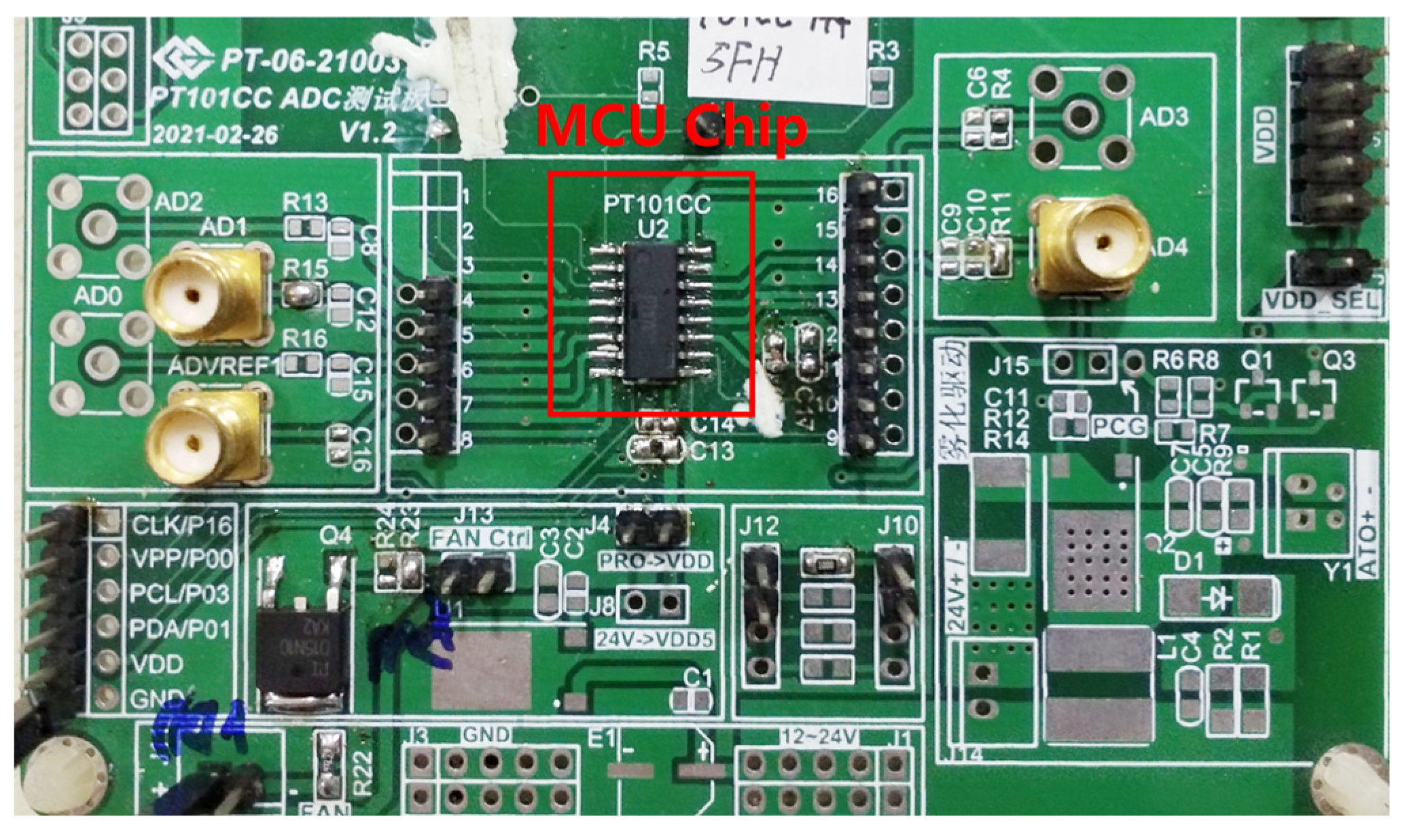
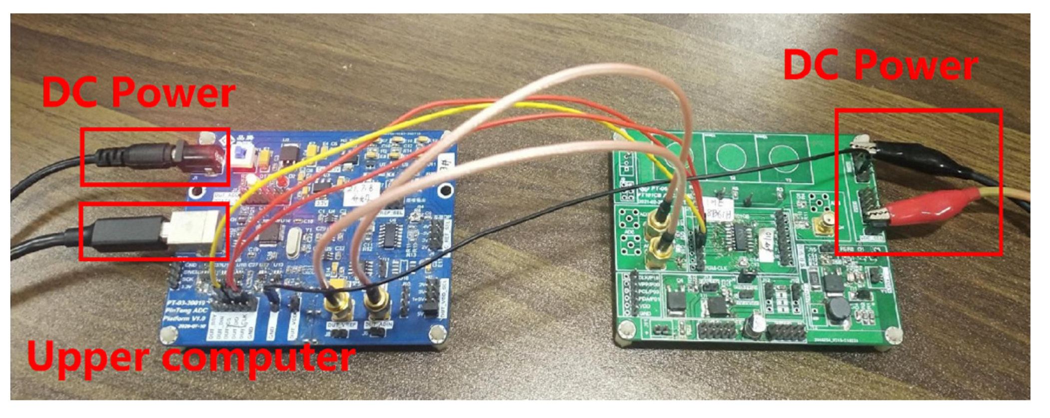
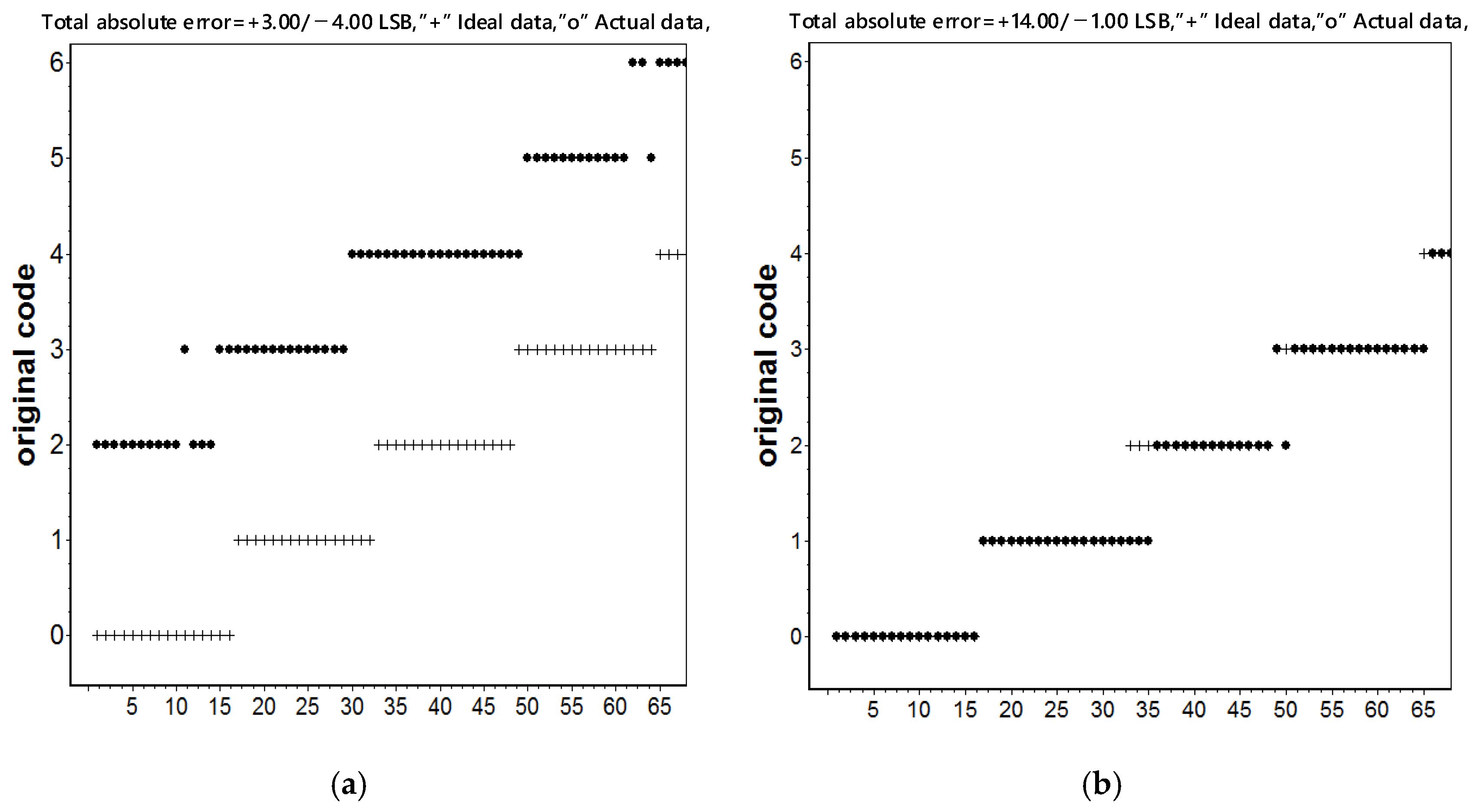
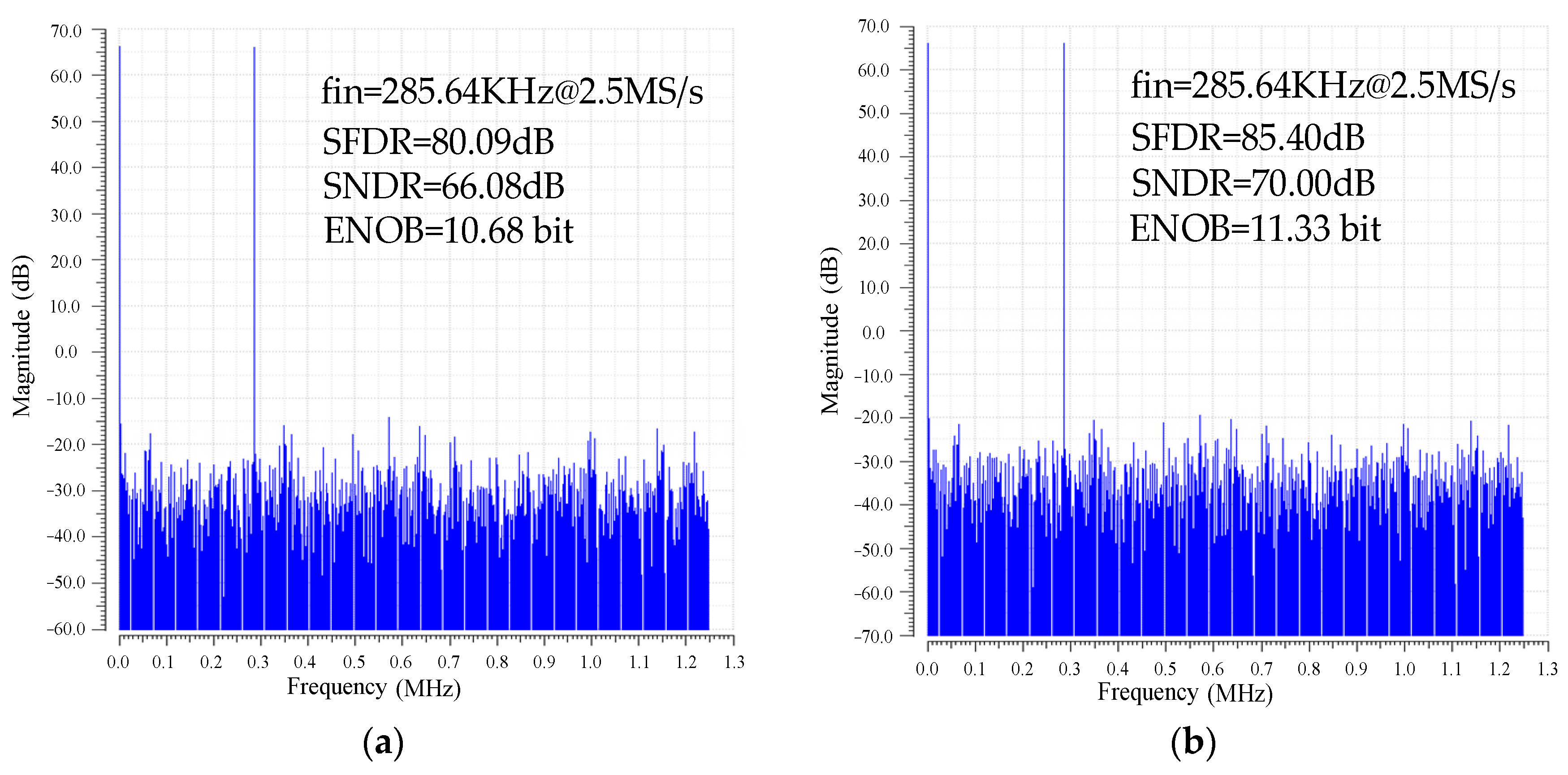
4.2. Implementation and Measurement of the Proposed Comparator

Two 12-bit SAR ADCs with and without a self-calibrated comparator were integrated into the two same-type MCU chips for testing, respectively. An MCU chip with the self-calibration comparator is named PT101CC, and another MCU chip without the self-calibration comparator is named PT101CB. Figure 18 shows the PT101CC and the printed circuit board (PCB) used for testing, and Figure 19 shows the PT101CB test environment.
After the obtained test data are analyzed and processed by computer software, the output waveforms of the two 12-bit SAR ADCs in the PT101CB and the PT101CC were obtained and are shown in Figure 20a,b respectively. “o” and “+” represent the measured output signal and the ideal output signal of the two 12-bit SAR ADCs, respectively. Figure 20 shows that when Vin = 0 V, the output of the PT101CB is code = 2, while the output of the PT101CC is code = 0. The minimum voltage detected by the ADC based on the proposed comparator with the self-calibration is 0 LSB, and the offset voltage can be eliminated effectively.
The output spectrum of the Nyquist frequency fast Fourier transform (FFT) spectrum for the 12-bit SAR ADC with and without calibration is shown in Figure 21. The improved ENOB and signal-to-noise plus distortion ratio (SNDR) are 11.33 bits and 70.00 dB, respectively, in Figure 21a with calibration, while the ENOB and SNDR are 10.68 bits and 66.08 dB, respectively, in Figure 21b without calibration. The ENOB and SNDR with calibration are increased by 0.65 bits and 3.92 dB, respectively.
The performance parameters of the proposed comparator with self-calibration designed in this study are compared with those of other similar comparators in Table 2. The proposed comparator improves the speed and accuracy of the comparator at the cost of the overall power consumption and meets the high-precision and high-speed requirements of touch MCU applications. The supplied voltage of the proposed comparator is 5 V, which is higher than that of other comparators, mainly to meet the requirement of a 5 V supply voltage for a touch MCU chip. Therefore, compared with the SAR ADCs in other studies, the power consumption of the designed SAR ADC is significantly increased, and the obtained figure of merit (FOM) 726.6 fJ/conversion-step is relatively high due to the increased power consumption and the static comparator topology adopted by the 12-bit SAR ADC in this study.

5. Conclusions

The design of a self-calibration comparator for a 12-bit SAR ADC applied in a touch MCU chip is presented in this paper. The common-mode voltage Vcm is set at VDD/2 to ensure that the flip time of the proposed comparator is as short as possible when the input voltage VINP is in the range of 0-VDD. A symmetrical OTA is adopted to improve the matching of differential input pairs and provide better offset and CMRR specifications. OOS and IOS cancellation, an offset trimming circuit, and self-calibration technology are proposed to improve the performance of the self-calibration comparator. The OOS and IOS cancellation technique is employed to reduce the input-referred offset voltage of seven-stage preamplifiers and OTA. The offset trimming circuit together with self-calibration technology is proposed to further suppress the residual offset of the comparator and compensate the conversion error caused by nonidealities in the SAR ADC system to a minimum. The simulation results show that the precision of the comparator is 30 μV and the power consumption is 4.58 mW at 5 V power supply voltage and 50 MHz clock. With a 5-bit digital controller, the offset trimming range and step size are ±9.15 mV and 0.61 mV, respectively. The proposed self-calibration comparator is also capable of calibrating conversion errors caused by line resistance in SAR ADC systems. The chip implementation and measurement results demonstrated that the ADC conversion error caused by a line resistor could be calibrated effectively.

Author Contributions

Conceptualization, J.T. and Y.W.; design, implementation, H.G. and Y.W.; measurement, Y.W.; writing—review and editing, all authors; supervision, J.T.; funding acquisition, J.T. All authors have read and agreed to the published version of the manuscript.

Funding

This research was funded by the Open Research Fund of Hunan Provincial Key Laboratory of Flexible Electronic Materials Genome Engineering under grant No. 202015.

Data Availability Statement

The data that support the findings of this study are available from the corresponding author upon reasonable request.

Acknowledgments

The MCU chips and testing equipment were supported by Hunan PinTeng Technology Co., Ltd., Changsha, China.

Conflicts of Interest

The authors declare no conflict of interest.

References

  1. Ali, K.; Teo, J.H.; Sarkar, S.; Alioto, M. Dual-Mode Conversion Gating, Comparator Merging, and Reference-Less Calibration for 2.7× Energy Reduction in SAR ADCs under Low-Activity Inputs. IEEE Solid-State Circuits Lett. 2023, 6, 57–60. [Google Scholar] [CrossRef]
  2. Ghasemi, R.; Karami, M.A. A low-power high-speed two-stage dynamic comparator with a new offset cancellation technique in 90 nm CMOS technology. In Proceedings of the 2020 28th Iranian Conference on Electrical Engineering (ICEE), Tabriz, Iran, 4–6 August 2020. [Google Scholar]
  3. Qiu, L.; Meng, T.; Yao, B.; Du, Z.; Yuan, X. A High-Speed Low-Noise Comparator with Auxiliary-Inverter-Based Common Mode-Self-Regulation for Low-Supply-Voltage SAR ADCs. IEEE Trans. Very Large Scale Integr. (VLSI) Syst. 2023, 31, 152–156. [Google Scholar] [CrossRef]
  4. Bandla, K.; Krishnan, A.H.; Sethi, S.; Pal, D. Design of High Speed and Low Offset SR Latch Based Dynamic Comparator. In Proceedings of the 2020 IEEE Region 10 Symposium (TENSYMP), Dhaka, Bangladesh, 5–7 June 2020. [Google Scholar]
  5. Campos, A.L.; Navarro, J.; Luppe, M. Design of a low power 10-bit 12 MS/s asynchronous SAR ADC in 65 nm CMOS. In Proceedings of the 2019 32nd Symposium on Integrated Circuits and Systems Design (SBCCI), Sao Paulo, Brazil, 26–30 August 2019; pp. 1–6. [Google Scholar]
  6. da Costa, J.P.D.C.; Gounella, R.H.; Bastos, W.B.; Longo, E.; Carmo, J.P. Photovoltaic Sub-Module with Optical Sensor for Angular Measurements of Incident Light. IEEE Sens. J. 2019, 19, 3111–3120. [Google Scholar] [CrossRef]
  7. Wang, T.Y.; Li, H.Y.; Ma, Z.Y.; Huang, Y.J.; Peng, S.Y. A Bypass-Switching SAR ADC with a Dynamic Proximity Comparator for Biomedical Applications. IEEE J. Solid-State Circuits 2018, 53, 1743–1754. [Google Scholar] [CrossRef]
  8. Enz, C.C.; Temes, G.C. Circuit techniques for reducing the effects of op-amp imperfections: Autozeroing, correlated double sampling, and chopper stabilization. Proc. IEEE 1996, 84, 1584–1614. [Google Scholar] [CrossRef]
  9. Cheng, Y.; Tong, Y. Techniques for offset calibration in comparators. In Proceedings of the 2021 International Conference on Electronic Information Engineering and Computer Science (EIECS), Changchun, China, 23–26 September 2021. [Google Scholar]
  10. Kouhalvandi, L.; Aygün, S.; Özdemir, G.G.; Güneş, E.O. 10-bit High-speed CMOS comparator with offset cancellation technique. In Proceedings of the 2017 5th IEEE Workshop on Advances in Information, Electronic and Electrical Engineering (AIEEE), Riga, Latvia, 24–25 November 2017. [Google Scholar]
  11. Razavi, B.; Wooley, B.A. Design techniques for high-speed, high-resolution comparators. IEEE J. Solid-State Circuits 1992, 27, 1916–1926. [Google Scholar] [CrossRef]
  12. Li, J.; Weisheng, X.; Youling, Y. A high-speed and high-resolution CMOS comparator with three-stage preamplifier. J. Semicond. 2010, 31, 045006. [Google Scholar] [CrossRef]
  13. Park, H.; Yu, C.; Kim, H.; Roh, Y.; Burm, J. Low Power CMOS Image Sensors Using Two Step Single Slope ADC with Bandwidth-Limited Comparators & Voltage Range Extended Ramp Generator for Battery-Limited Application. IEEE Sens. J. 2020, 20, 2831–2838. [Google Scholar]
  14. Li, W.; Li, F.; Liu, J.; Li, H.; Wang, Z. A 13-bit 160MS/s pipelined subranging-SAR ADC with low-offset dynamic comparator. In Proceedings of the 2017 IEEE Asian Solid-State Circuits Conference (A-SSCC), Seoul, Republic of Korea, 6–8 November 2017. [Google Scholar]
  15. Chen, Y.; Wang, Z.; Zhuang, Y.; Tang, H. Analysis and Design of Sigma-Delta ADCs for Automotive Control Systems. In Proceedings of the 2021 IEEE 3rd International Conference on Circuits and Systems (ICCS), Chengdu, China, 29–31 October 2021. [Google Scholar]
  16. Pei, R.; Liu, J.; Tang, X.; Li, F.; Wang, Z. A low-offset dynamic comparator with input offset-cancellation. In Proceedings of the 2017 IEEE 12th International Conference on ASIC (ASICON), Guiyang, China, 25–28 October 2017. [Google Scholar]
  17. Fan, X.P.; Chan, P.K. A CMOS high-speed multistage preamplifier for comparator design. In Proceedings of the 2004 IEEE International Symposium on Circuits and Systems (IEEE Cat. No. 04CH37512), Vancouver, BC, Canada, 23–26 May 2004. [Google Scholar]
  18. Lee, M.J.; Dally, W.J.; Chiang, P. Low-power area-efficient high-speed I/O circuit techniques. IEEE J. Solid-State Circuits 2000, 35, 1591–1599. [Google Scholar] [CrossRef]
  19. Jung, H.; Youn, E.; Jang, Y.C. An 11-Bit 10 MS/s SAR ADC with C–R DAC Calibration and Comparator Offset Calibration. Electronics 2022, 11, 3654. [Google Scholar] [CrossRef]
  20. Xu, Y.; Belostotski, L.; Haslett, J.W. Offset-corrected 5GHz CMOS dynamic comparator using bulk voltage trimming: Design and analysis. In Proceedings of the 2011 IEEE 9th International New Circuits and Systems Conference, Bordeaux, France, 26–29 June 2011. [Google Scholar]
  21. Wang, S.-H.; Hung, C.-C. A 0.3V 10b 3MS/s SAR ADC with Comparator Calibration and Kickback Noise Reduction for Biomedical Applications. IEEE Trans. Biomed. Circuits Syst. 2020, 14, 558–569. [Google Scholar] [PubMed]
  22. Lee, J.; Lim, Y.; Sung, B.; Oh, S.; Chun, J.H.; Lee, J. An Effective Transconductance Controlled Offset Calibration for Dynamic Comparators. In Proceedings of the 2020 IEEE International Symposium on Circuits and Systems (ISCAS), Seville, Spain, 10–21 October 2020. [Google Scholar]
  23. Mohammadi, M.; Sadeghipour, K.D. A 0.5V 200 MHz offset trimmable latch comparator in standard 0.18 um CMOS process. In Proceedings of the 2013 21st Iranian Conference on Electrical Engineering (ICEE), Mashhad, Iran, 14–16 May 2013. [Google Scholar]
  24. Verma, D.; Shehzad, K.; Khan, D.; Kim, S.J.; Pu, Y.G.; Yoo, S.-S.; Hwang, K.C.; Yang, Y.; Lee, K.-Y. A Design of Low-Power 10-bit 1-MS/s Asynchronous SAR ADC for DSRC Application. Electronics 2020, 9, 1100. [Google Scholar] [CrossRef]
  25. Baek, S.-Y.; Lee, J.-K.; Ryu, S.-T. An 88-dB max-SFDR 12-bit SAR ADC with speed enhanced ADEC and dual registers. IEEE Trans. Circuits Syst. II Exp. Briefs 2013, 60, 562–566. [Google Scholar] [CrossRef]
  26. Behzad, R. Design of Analog CMOS Integrated Circuits; Mc-Graw Hill Inc.: New York, NY, USA, 2015. [Google Scholar]
  27. Hesham, O. Fast and accurate technique for comparator offset voltage simulation. Microelectron. J. 2019, 89, 91–97. [Google Scholar]
  28. Peng, X.; Gao, A.; Chen, Z.; Zhang, H.; Li, Y.; Cao, W.; Liu, X.; Tang, H. A Novel Comparator Offset Calibration Technique for SAR ADCs. In Proceedings of the 2018 IEEE International Conference on Electron Devices and Solid State Circuits (EDSSC), Shenzhen, China, 6–8 June 2018. [Google Scholar]
  29. Zhang, Y.; Cai, J.; Li, X.; Zhang, Y.; Su, B. A 3.66 μW 12-bit 1 MS/s SAR ADC with mismatch and offset foreground calibration. Microelectron. J. 2021, 116, 105–244. [Google Scholar] [CrossRef]
Figure 1. The structure of the proposed self-calibration comparator applied in an SAR ADC system.
Electronics 12 02277 g001
Figure 2. The common-mode buffer.
Electronics 12 02277 g002
Figure 3. The symmetrical OTA.
Electronics 12 02277 g003
Figure 4. Differential preamplifier Ai (i = 0, 2, …, 5, 6).
Electronics 12 02277 g004
Figure 5. Comparator offset cancellation techniques: (a) the output offset storage; (b) the input offset storage.
Electronics 12 02277 g005
Figure 6. Differential preamplifier with offset voltage.
Electronics 12 02277 g006
Figure 7. The first-stage preamplifier A0 with offset trimming circuits.
Electronics 12 02277 g007
Figure 8. Control logic circuit.
Electronics 12 02277 g008
Figure 9. Circuit implementation of the switches S0, S1, and S2.
Electronics 12 02277 g009
Figure 10. The timing diagram of comparator offset trimming.
Electronics 12 02277 g010
Figure 11. The layout of the comparator.
Electronics 12 02277 g011
Figure 12. Amplitude–frequency response curves of all amplifiers. (a) preamplifier A0; (b) preamplifier Ai (i = 1, 2, …, 5, 6); (c) OTA.
Electronics 12 02277 g012
Figure 13. Transient simulation test bench of the proposed comparator.
Electronics 12 02277 g013
Figure 14. Transient simulation curves of the proposed comparator (ripple = 30 μV).
Electronics 12 02277 g014
Figure 15. Transient simulation curves of the proposed comparator (ripple < 30 μV).
Electronics 12 02277 g015
Figure 16. The proposed self-calibration comparator in a 12-bit SAR ADC system.
Electronics 12 02277 g016
Figure 17. Flow chart of self-calibration algorithm.
Electronics 12 02277 g017
Figure 18. The MCU chip and printed circuit board for testing.
Electronics 12 02277 g018
Figure 19. Test environment of implemented MCU chip.
Electronics 12 02277 g019
Figure 20. A/D conversion result of the two MCU chips: (a) without calibration; (b) with calibration.
Electronics 12 02277 g020
Figure 21. Output spectrum of the 12-bit SAR ADC: (a) without calibration; (b) with calibration.
Electronics 12 02277 g021
Table 1. The 5-bit digital controller code and corresponding offset variation.
OPT<4:0> CodeOffset Variation (LSB)OPT<4:0> CodeOffset Variation (LSB)
000000100000
00001+0.510001−0.5
00010+110010−1
00011+1.510011−1.5
00100+210100−2
00101+2.510101−2.5
00110+310110−3
00111+3.510111−3.5
01000+411000−4
01001+4.511001−4.5
01010+511010−5
01011+5.511011−5.5
01100+611100−6
01101+6.511101−6.5
01110+711110−7
01111+7.511111−7.5
Table 2. Comparison of SAR ADC performance between this study and other studies.
ParametersThis Work[19][24][26][28]
Technology method (nm)951805535055
Supplied voltage (V)51.812.3-
Fs (MS/s)2.51013100
Resolution (bit)1211101210
Power (μW)458058314.812304400
Area (mm2)0.1730.29-0.340.052
ENOB (bit)11.3310.39.74-9.52
SFDR (bit)85.4078.57-70.169.03
SNDR (dB)7063.7760.3962.759.11
FoMw * (fJ/Conv. step)726.646.217.336859.9
* FoMw = Power/(Fs × 2ENOB).
Disclaimer/Publisher’s Note: The statements, opinions and data contained in all publications are solely those of the individual author(s) and contributor(s) and not of MDPI and/or the editor(s). MDPI and/or the editor(s) disclaim responsibility for any injury to people or property resulting from any ideas, methods, instructions or products referred to in the content.

