Article

Thirteen-Level Switching Capacitor Inverter with Six Times Boost and Self-Balancing Capability

School of Electrical and Information Engineering, Hunan University of Technology, Zhuzhou 412007, China
*
Author to whom correspondence should be addressed.
Electronics 2023, 12(10), 2259; https://doi.org/10.3390/electronics12102259
Submission received: 6 March 2023 / Revised: 21 April 2023 / Accepted: 28 April 2023 / Published: 16 May 2023
(This article belongs to the Section Networks)

Abstract

:
A thirteen-level inverter based on switching capacitor is proposed in order to improve the boost capacity and output power quality of inverter in renewable energy power generation system. The proposed topology is composed of one DC input power supply, three capacitors and 14 switching devices, and achieves thirteen-level output with six times voltage boost. It has smaller volume, lower cost and output harmonic content. Moreover, it can realize inverter without H bridge and reduce the voltage stress of switching tube. In addition, the proposed inverter can achieve self-balancing capacitor voltage without any auxiliary method, simplifying the complexity of control. The superiority of the proposed topology is verified by comparing with other traditional multilevel inverters. The simulation and experimental verification on the simulation and prototype platform show that the inverter has good performance in both steady and dynamic conditions.

1. Introduction

Nowadays, multi-level inverters (MLI) play an important role in modern power systems and have many advantages, such as avoiding high-voltage stress under high switching frequency operation and producing output voltage with low total harmonic distortion [1,2,3,4]. Therefore, the research and application of multilevel inverters are continuing [5,6,7,8].
In recent years, the dominant multilevel inverters include neutral clamped (NC), flying capacitor (FC) and cascaded H-bridge (CHB) [9,10]. Among them, the NC circuit and FC circuit are limited by capacitor voltage imbalance and the number of switching devices. In contrast, the CHB circuit has a simple structure, but multiple independent DC power supplies are required for cascading [11]. In addition, most traditional multilevel inverters need to add an additional boost circuit at low-voltage input, which increases the volume of the inverter and reduces the economy. In order to alleviate the above problems, researchers proposed a switched capacitor multilevel inverter (SC-MLI) [12,13,14]. SC-MLI not only has the characteristics of self-balancing, but also can achieve more level output with fewer devices and it also has the ability to boost independently [15]. Therefore, domestic and foreign researchers continue to innovate and improve it [16,17,18].
The topology proposed in Reference [19] can achieve the effect of increasing the voltage gain and the number of output levels, but the number of devices used is large, and the terminal H-bridge needs to withstand large voltage stress and cannot be applied in high-voltage output occasions. In order to reduce the number of devices, Reference [20] proposed a nine-level SC-MLI, greatly reducing the number of switching devices, but its topology is not conducive to the expansion of the inverter bridge, the output level is limited. References [21,22,23,24] proposed an extensible SC-MLI, which achieves more levels and higher gain output by cascading multiple modules with capacitors in the topology. However, the number of output levels of the inverter in Reference [21] is linked to the number of DC power supplies, which limits the number of output levels. The inverter proposed in [22] not only needs multiple DC power supplies, but also needs to set the voltage ratio between multiple power supplies. The MLI in Reference [23] requires a large number of devices and a relatively complex structure, so the volume and cost of the system are relatively high. The topology proposed in [24] only requires a single DC source, which is simple in structure and easy to expand. However, when there are too many expansion modules, the number of levels does not increase any more, and the economy is low.
In order to solve the above problems, this paper proposes a thirteen-level SC-MLI with expansion capability. The capacitor is periodically charged and discharged so that the voltage inside the capacitor can be self-balanced. Through the series-parallel combination of the dual-capacitor basic module of the front stage and the expansion module of the rear stage, the post-stage capacitor is charged and discharged at the same time as the post-stage capacitor to supply energy to the load. The inverter can achieve more level output with fewer devices, and has the ability of independent boost, which greatly reduces the cost of the system and greatly expands the application range.

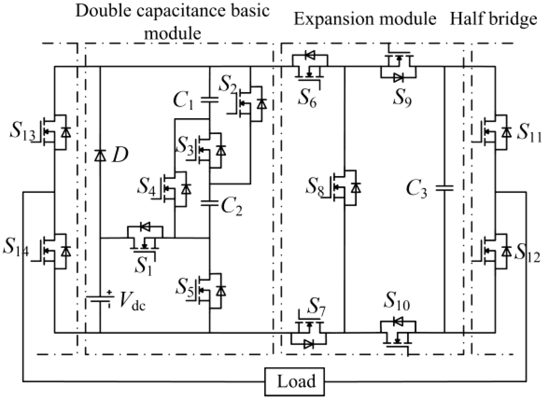
2. Proposed Topology

2.1. Description of the Proposed MLI

The main circuit topology of the proposed thirteen-level inverter is shown in Figure 1, including double capacitance base module, extended module and half-bridge module.
In the proposed topology, the output voltage is superimposed by a power supply and a capacitor. In the dual-capacitor basic module, the DC power supply Vdc charges the capacitors C1 and C2; the switch tubes S2 and S4 are jointly switched on and off, and are complementary to S3 to change the series and parallel connection of capacitors C1 and C2. The switch tube S1 and S5 are complementary conduction, switching the series and parallel connection between DC power supply Vdc and capacitor C1 and C2. During the charging and discharging process, the states of C1 and C2 capacitors are completely consistent, thus solving the problem of capacitor voltage balance. In addition, the dual capacitor module and the capacitor C3 are connected by an expansion module composed of five switches S6~S10; finally, the half-bridge structure composed of two sets of switch tubes replaces the H-bridge to change the polarity of its output.
The inverter uses a DC input power supply, three capacitors and fourteen switching devices (such as MOSFETE) to achieve a step wave output of up to thirteen levels, with six times the voltage gain. The maximum blocking voltage (MBV) of all switches in the dual-capacitor module is equal to Vdc. The maximum blocking voltage of the expansion module and the switches in the two half-bridges is 3Vdc, so the total standing voltage (TSV) of the fourteen switches is 32Vdc.

2.2. Steady-State Switching Analysis of the Proposed MLI

Figure 2 shows the inverter in the positive half cycle different output level working state, black solid line for the circuit discharge circuit.
In order to simplify the analysis, the on-resistance of the switch tube and the voltage drop of the capacitor voltage in the circuit are ignored. The working principle of the inverter in the positive half cycle is analyzed as follows.
(1)
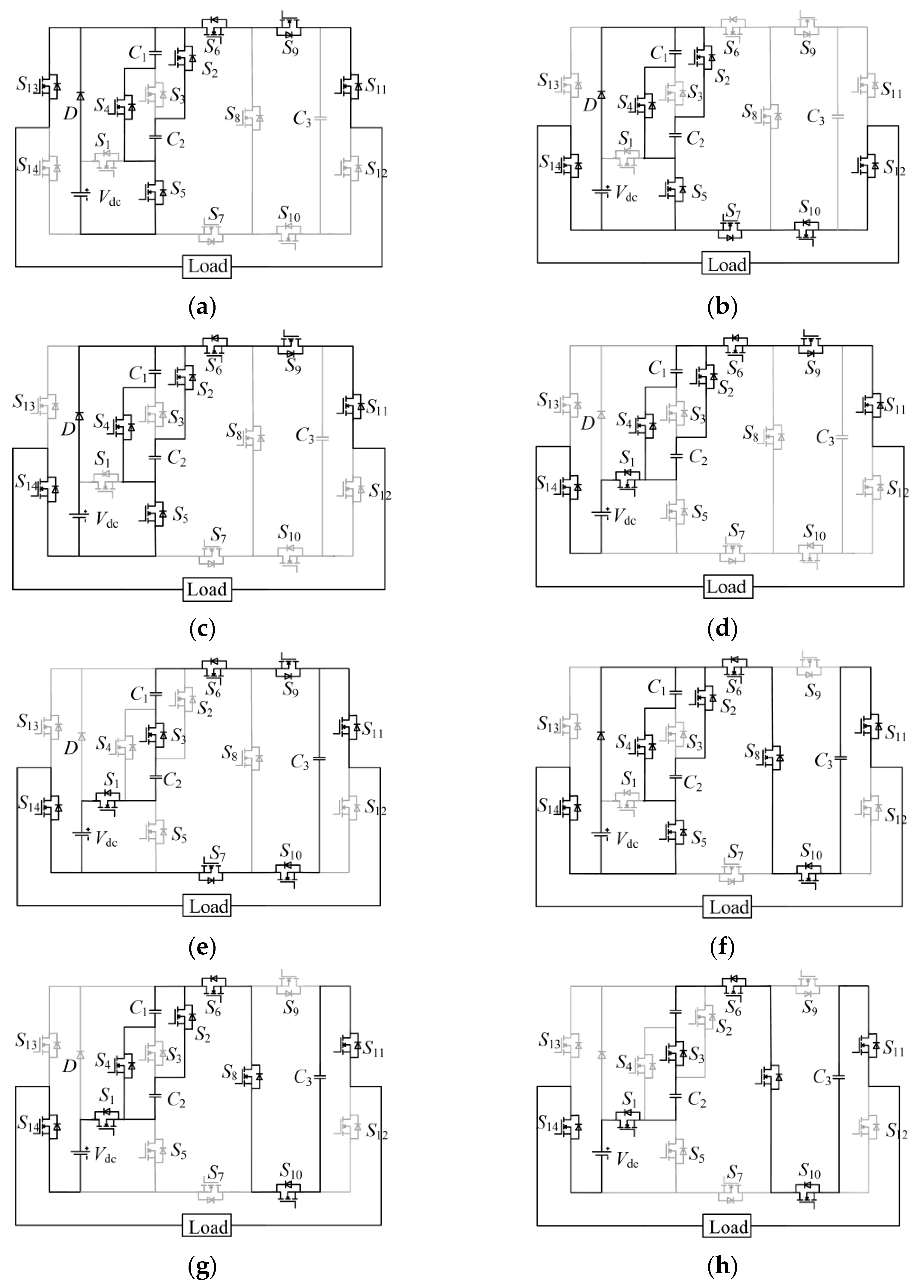
Working mode 1 (Vo = 0), as shown in Figure 2a. In the dual-capacitor module, the switch tubes S2, S4 and S5 are turned on, the capacitors C1 and C2 are connected in parallel, and the DC power supply is connected in parallel with the capacitors C1 and C2 and charged to Vdc. In the expansion module, the switches S6 and S9 are turned on, and the dual-capacitor module discharges separately. In the half-bridge circuit structure, the switch tubes S11 and S13 are conductive. Similarly, the case of obtaining zero level in the negative half cycle is shown in Figure 2b.
(2)
Working mode 2 (Vo = +Vdc), as shown in Figure 2c. The state of each element in the dual capacitor module is the same as in Mode 1. In the expansion module, the switches S7 and S10 are turned on, and the dual-capacitor module discharges separately. In the half-bridge circuit structure, the switch tubes S12 and S14 are conductive.
(3)
Working mode 3 (Vo = +2Vdc), as shown in Figure 2d. In the dual-capacitor module, the capacitor C1 and C2 are connected in parallel and connected in series with the DC power supply to provide energy to the load. The switches S7 and S10 in the expansion module are conductive, and the double capacitor module discharges separately. In the half-bridge circuit structure, the switch tubes S12 and S13 are conductive.
(4)
Working mode 4 (Vo = +3Vdc), as shown in Figure 2e. In the double capacitor module, the switch tubes S1 and S3 are turned on, and the capacitor C1 and C2 are connected in series to provide energy to the load together with the DC power supply. The four switches S6, S7, S9 and S10 in the expansion module are switched on together, and the dual capacitor module charges the capacitor C3 to 3Vdc. In the half-bridge circuit structure, the switch tubes S11 and S14 are conductive.
(5)
Operating Mode 5 (Vo = +4Vdc), as shown in Figure 2f. In the dual-capacitor module, the switch tubes S2, S4 and S5 are turned on together. At this time, the capacitors C1 and C2 are connected in parallel, and then charged in parallel with the DC power supply to Vdc. The switches S7, S8 and S9 in the expansion module are turned on, and the dual-capacitor module discharges in series with the capacitor C3. In the half-bridge circuit structure, the switch tubes S11 and S14 are conductive.
(6)
Working mode 6 (Vo = +5Vdc), as shown in Figure 2g. In the dual-capacitor module, the switch tubes S1, S2 and S4 are turned on. After the capacitors C1 and C2 are connected in parallel, they are connected in series with the DC power supply to provide energy to the load. In the expansion module, the switch tubes S7, S8 and S9 are switched on, and the double capacitor module discharges in series with the capacitor C3. In the half-bridge circuit structure, the switch tubes S11 and S14 are conductive.
(7)
Working mode 7 (Vo = +6Vdc), as shown in Figure 2h. In the double capacitor module, the switch tubes S1 and S3 are connected, the capacitors C1 and C2 are connected in series, and the DC power supply is connected in series to provide energy to the load, and the diode D is cut off in reverse. In the expansion module, the switch tubes S7, S8 and S9 are turned on together, and the double capacitor module is discharged in series with the capacitor C3. In the half-bridge circuit structure, the switch tubes S11 and S14 are conductive. The working principle of the inverter working in the negative half cycle is consistent with that in the positive half cycle.
Table 1 shows the charging, discharging and idle state of the capacitor under different switching modes.

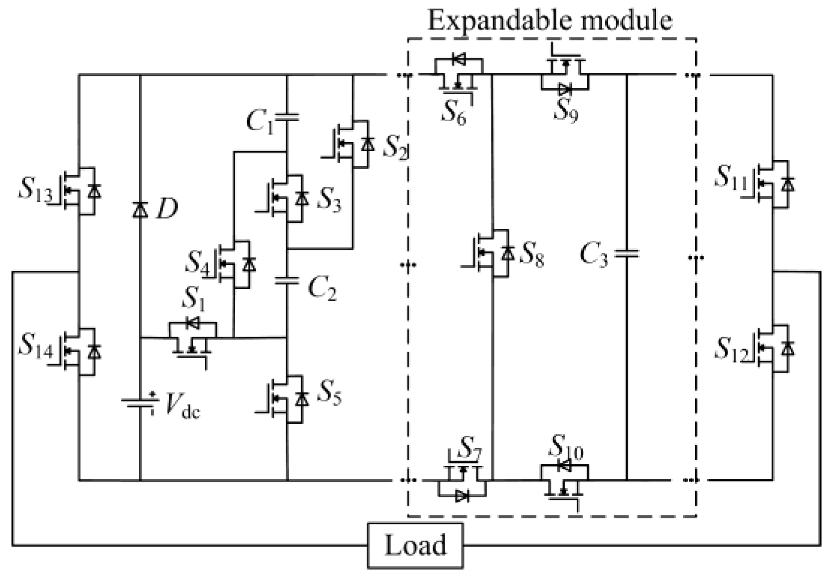
2.3. Proposed N-Level Topology

In order to increase the number of output levels of the proposed topology and improve the gain of its output voltage, multiple expansion modules are added to expand the circuit on the basis of the original inverter, as shown in Figure 3. In the dotted box is the expandable capacitor module. After adding the expandable module, the working principle of the inverter is similar to the structure of the only expandable module.
For each single capacitor module added to the extended structure, the voltage gain of the inverter circuit will increase by 3Vdc and the number of levels will increase by six. So, when the module is m, the inverter circuit voltage gain will increase 3mVdc, the output level is:
N = 6 m + 7
In the expansion module, the capacitors in the adjacent modules can discharge in parallel, so the voltage ripple of the capacitor is further improved.

3. Modulation and Characteristic Strategy

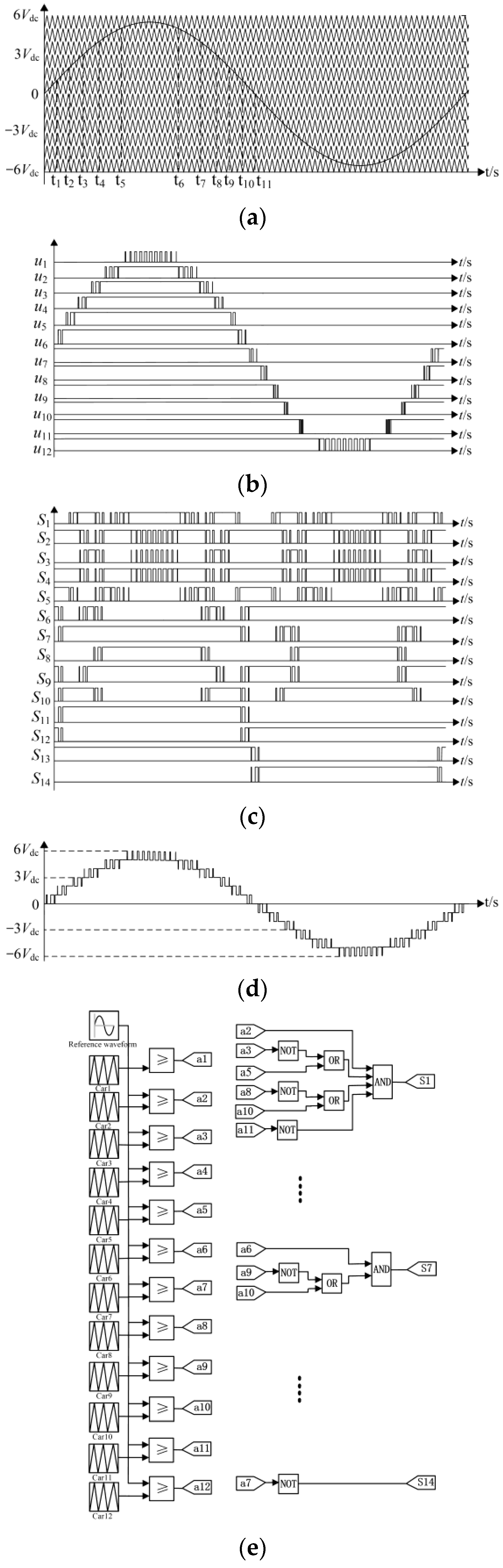
3.1. Modulation Strategy

According to the analysis of the working principle of the thirteen-level inverter mentioned above, this paper adopts the carrier phase stacking control method with better harmonic elimination effect, and its principle is shown in Figure 4.
In Figure 4, twelve groups of triangular carriers with an amplitude of Ac and a frequency of fc are compared sine waves with amplitude A and frequency f, as shown in Figure 4a. The original PWM pulses of u1~u12 are obtained, as shown in Figure 4b. Modulation ratio M is:
M = A c 6 A
This paper sets the modulation ratio to 0.9. Twelve original pulses are combined into a control signal of fourteen switching tubes according to a specific logical relationship, as shown in Figure 4c. In one cycle, the logical relationship between each switch and the twelve original pulses is:
S 1 = u 2 + u ¯ 3 u 4 + u ¯ 4 u 5 + u ¯ 8 u 9 + u ¯ 9 u 10 + u ¯ 11
S 2 = u 1 u ¯ 2 + u ¯ 2 u 3 + u ¯ 4 u 9 + u ¯ 10 u 11 + u ¯ 11 u 12
S 3 = S ¯ 2
S 4 = S 2
S 5 = u ¯ 2 u 3 + u ¯ 5 u 8 + u ¯ 10 u 11
S 6 = u ¯ 3 u 4 + u ¯ 6
S 7 = u 6 + u ¯ 9 u 10
S 8 = u 3 + u ¯ 10
S 9 = u 4 + u ¯ 6 u 10
S 10 = u ¯ 3 u 6 + u ¯ 9
S 11 = u ¯ 6
S 12 = u 6
S 13 = u 7
S 14 = u ¯ 7
Figure 4e shows the logic circuit of grid pulse generated by carrier in-phase cascade control method. After the logical combination of the original pulses generated by the comparison between the sine wave and the twelve groups of carriers, fourteen groups of pulses are generated to drive the opening and closing of each switching tube of the inverter.

3.2. Analysis of Capacitor Balancing

Capacitance voltage self-balance is a prerequisite for normal operation of SC-MLI. If the capacitor voltage cannot achieve self-balancing, it will cause the voltage offset to fail to achieve the expected experimental results, and even damage the device.
According to Table 1, capacitors C1 and C2 operate in the same state, thus satisfying the condition that their capacitor voltages can be self-balanced. When the output voltage is 0, ±Vdc and ±4Vdc, the DC power supply charges the capacitors C1 and C2; when the output voltage becomes ±2Vdc and ±5Vdc, capacitors C1 and C2 discharge together in parallel; when the output voltage is ±3Vdc and ±6Vdc, the capacitor C1 and C2 discharge together in series. Therefore, capacitors C1 and C2 are always in a running state. Capacitor C3 charges and discharges alone, so there is no need to consider its capacitor voltage self-balancing. When the output voltage is 0, ±Vdc and ±2Vdc, the capacitor C3 is in an idle state; when the output voltage is ±3Vdc, C3 is charged in parallel with the capacitor basic module; when the output voltage is ±4Vdc, ±5Vdc and ±6Vdc, C3 discharges in series with the capacitor base module.

3.3. Analysis of the Capacitors

The output voltage of MLI is essentially a combination of power supply voltage and capacitor voltage in series and parallel, so the ripple of capacitor voltage plays a vital role in the quality of output power. Usually, the ripple is expressed as the amount of continuous discharge of the capacitor:
Δ Q c = t a t b I o sin ( 2 π f t φ ) dt
where, △Qc is the change value of the capacitance charge in the time period ta~tb, Io is the amplitude of the circuit output current, f is the load frequency and φ is the phase difference between the output voltage of the inverter with inductive load and the load current.
The capacitance voltage ripple △Uc is calculated from the capacitance discharge:
Δ U c = Δ Q c C
Under normal circumstances, the constraint voltage ripple is less than 10% of the rated voltage of the capacitor to avoid the adverse effects of the voltage ripple on the inverter. The conditions that the capacitor and the rated voltage Uc should meet are:
U c C 10 Δ Q c
The amplitude of the carrier wave obtained from Equation (2) is:
A c = A 6 M
As shown in Figure 4a, the instantaneous value of the output voltage of the inverter, the time period from 0 to Vdc is 0~t1, then:
t 1 = arcsin 1 6 M 2 π f
Similarly, when n = 1, 2, …, 6.
t n = arcsin n 6 M 2 π f
It can be seen from Table 1 and Figure 4 that when the continuous discharge of capacitors C1 and C2 is in the t2~t3 and t5~t6 time periods, the discharge amounts can be obtained as follows:
Δ Q c = t 2 t 3 I o sin ( 2 π f φ ) dt
Δ Q c = t 5 t 6 I o sin ( 2 π f φ ) dt
During a power frequency cycle, the amount of discharge from the capacitor C1 and the capacitor C2 is equal. Capacitor C3 in the t4~t6 period of continuous discharge, discharge capacity:
Δ Q c = t 4 t 6 I o sin ( 2 π f φ ) dt
According to the expressions (18)–(20), the variation of the charge of the capacitors C1 and C2 is less than that of C3 within half a cycle, so the voltage ripple of the two capacitors is less than that of C3.

3.4. Power Loss Calculation

The main losses of SC-MLI are capacitor ripple loss (Prip), conduction loss (Pcom) and switching loss (Psw). Prip is caused by the voltage fluctuation of the capacitor. According to Formula (18):
P rip = f o Δ Q c 2 C
The conduction loss of the inverter is caused by the parasitic parameters of the device, such as the on-resistance (rs) of the switch and the equivalent series resistance (ESR) of the capacitor. The equivalent parameters of the six working modes are shown in Table 2. The value of j in the table indicates that the output Vo is j times the Vdc.
According to Figure 4, in the interval [0, t1], the power loss of the output level between 0 and Vdc can be calculated by the following formula:
P 0 & V dc = 0 t 1 [ I o sin ( 2 π f o t ) ] 2 × [ ( E R S c + 6 r s ) A sin ( 2 π f o t ) A c ] + 4 r s ( 1 A sin ( 2 π f o t ) A c ) dt
Similarly, the power loss of the other five operating modes can also be obtained in the same way. Thus, Pcom can be obtained by:
P con = 4 ( P 0 & V dc + P V dc & 2 V dc + P 2 V dc & 3 V dc + P 3 V dc & 4 V dc + P 4 V dc & 5 V dc + P 5 V dc & 6 V dc )
Based on the charge and discharge process of the parasitic capacitor in the switching tube, assuming that the capacitance of the parasitic capacitor is linear, the voltage is gradually charged to vs. when the switch is turned off, where vs. is the MBV of the switch. Therefore, Psw is:
P sw = C s V s 2 f s
where, fs is the switching frequency of the switch, and is:
f s = N s f o
where, Ns is the switch transition in one cycle of the reference waveform. As you can see from Figure 4, the switch is repeatedly switched on and off at corresponding intervals. If the switch operates throughout the cycle, the Ns of each switch can be roughly calculated as the ratio of fs to fo. Therefore, Ns of each switch is:
N s = t s f c T s f o
where: ts is the working time of the switch; Ts is the time of a cycle.
Therefore, the efficiency of the inverter proposed is:
η = P o P o + P rip + P com + P sw
where, η and Po are respectively the efficiency and output power of the proposed inverter.

4. Comparison Outcomes

In order to highlight the overall advantages of the thirteen-level inverter, the proposed topology is compared with the existing typical topology. The topology of the contrast does not increase the expansion structure to ensure that the contrast is more distinct. The detailed comparison parameters are shown in Table 3, including the number of capacitors, switches, DC power supplies, MBV and TSV of each inverter.
It can be seen from Table 2 that although the number of switching tubes and TSV used in Reference [25] are comparable to those in this paper, its MBV is relatively high and two power supplies are used. Reference [26] reduced the number of power supplies and MBV, but the number of capacitors and switches is too large, TSV is too large. Reference [27] the MBV of the switch tube is less than this article, but the corresponding number of devices also increased, especially the use of five capacitors, which will increase the volume and cost of the inverter. In reference [28], the number of switching devices and the total voltage stress are relatively lower without using capacitors, but the number of power supplies increases linearly with the output voltage level. The MBV and TSV in References [29,30] are comparable to those in this paper, but the number of capacitors, switches and power supplies are slightly higher than those in this paper.
In summary, the topology proposed in this paper has obvious advantages in comprehensive performance, and also has the ability to expand, so it has good economy and practical application ability.

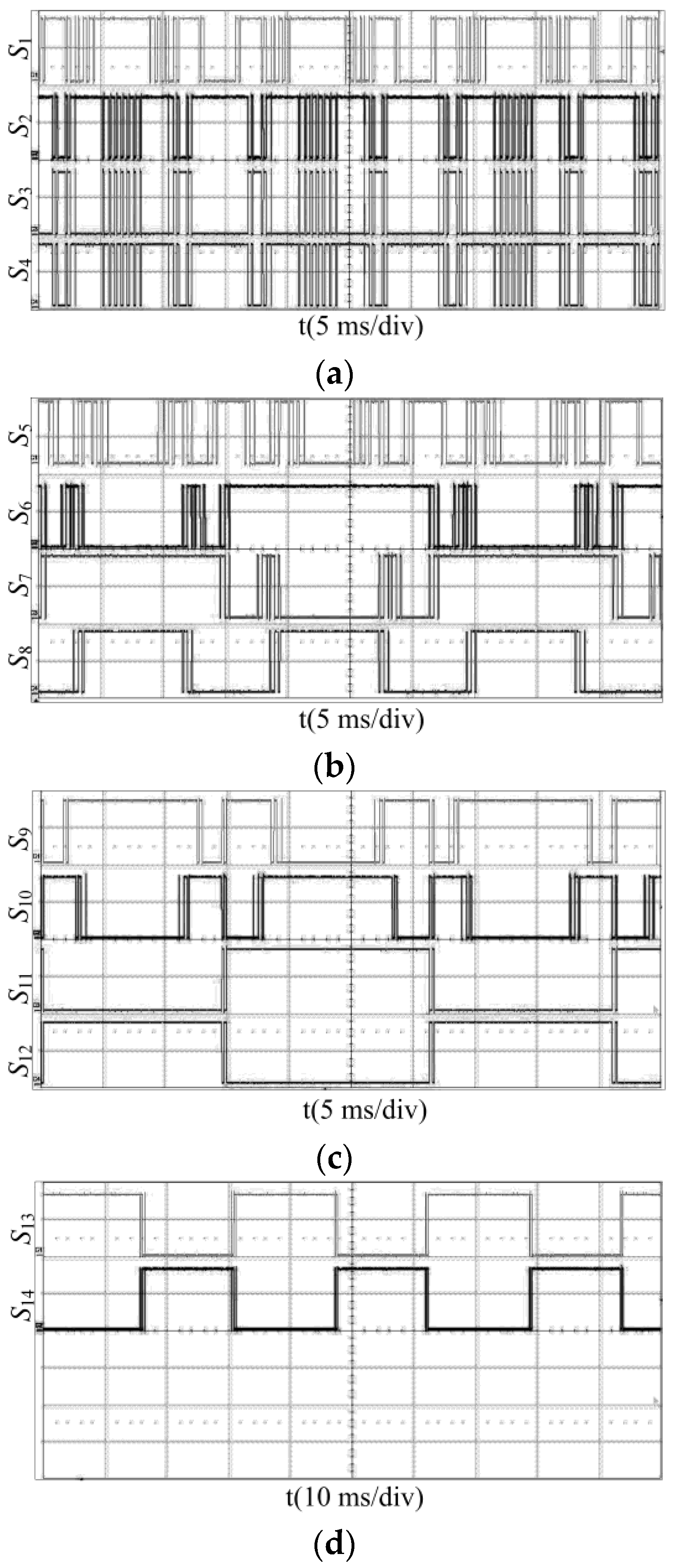
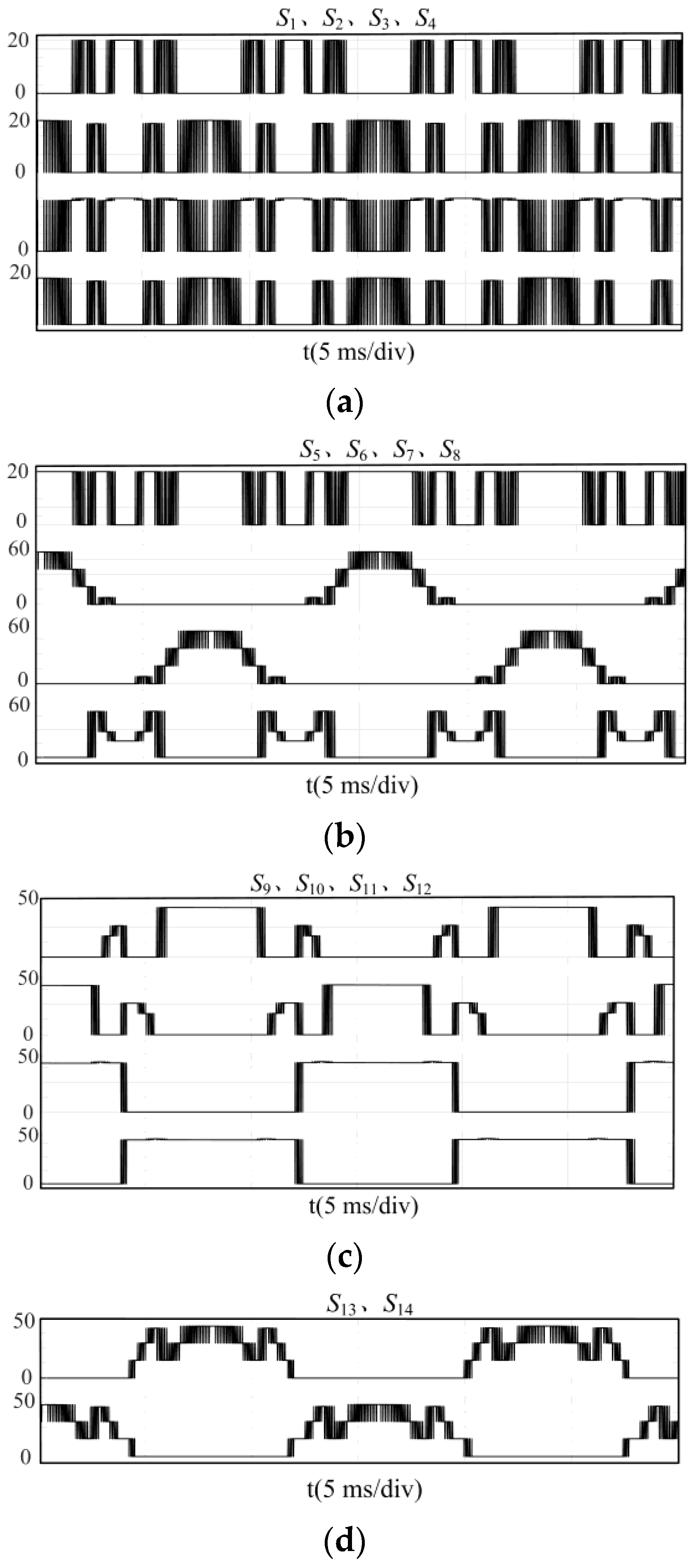
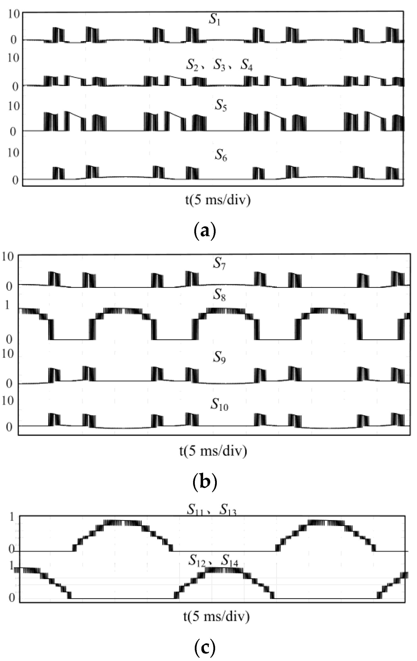
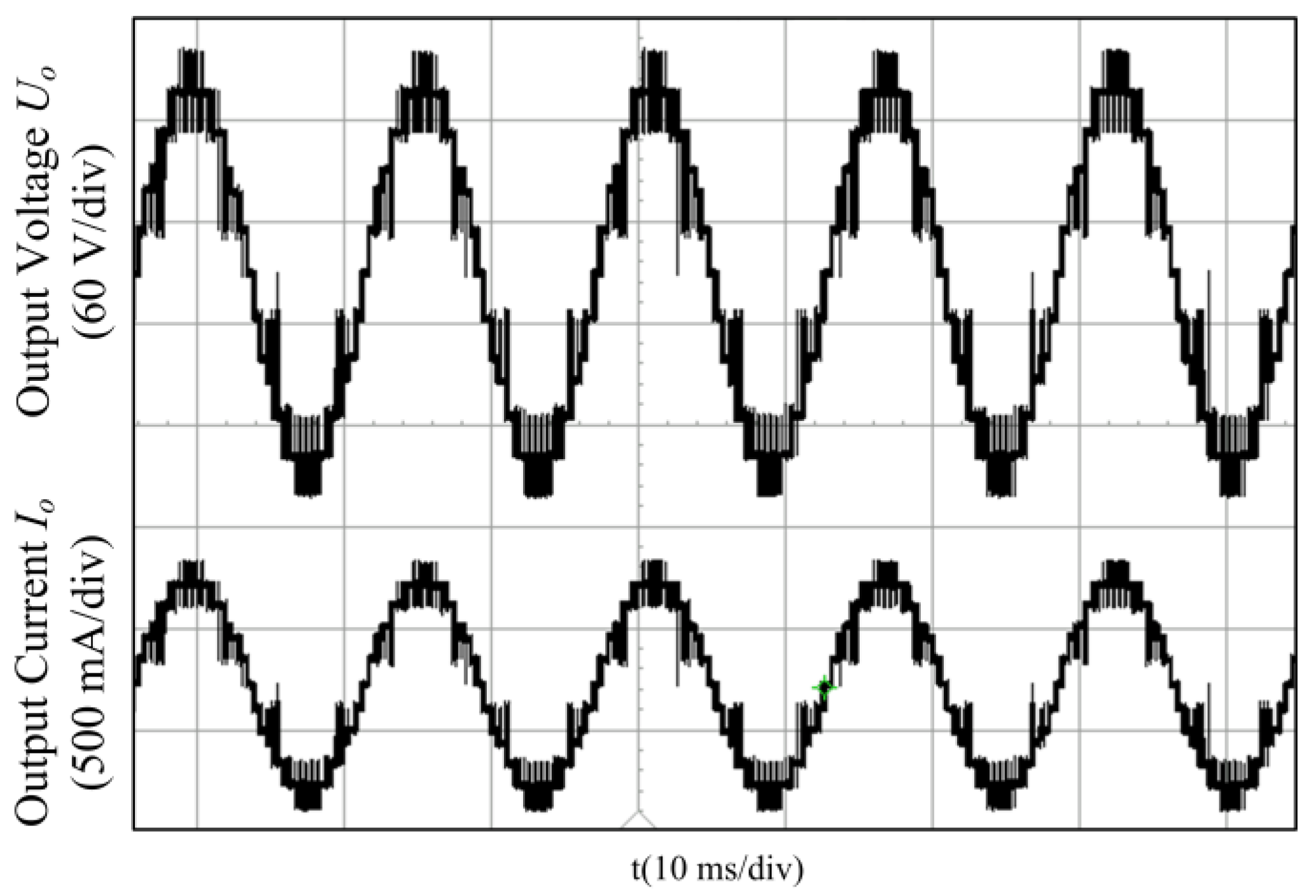
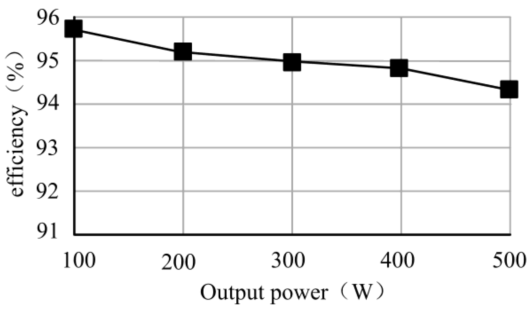
5. Simulation Verification and Experimental Verification

5.1. Simulation Verification

In order to verify the correctness of the thirteen-level switching capacitor inverter and the theory in this paper, the topology simulation circuit model is built on the Matlab/Simulink platform. The steady-state output voltage and current output waveform are shown in Figure 5.
The values of capacitors C1~C2 and C3 are 2200 uF and 4700 uF, Vin is 10 V, and pure resistance load R is 100 Ω. As can be seen in the figure, the output voltage is 60 V, and a level thirteen-step wave with six times gain is achieved.
For further analysis, the performance of the proposed topology under group load is analyzed. When the load is R = 100 Ω, L = 40 mH resistive load, the voltage and current output waveform is shown in Figure 6.
As can be seen from the figure, the output voltage is a standard thirteen-level step wave. According to the filter effect of inductance, the load current waveform is similar to sinusoidal waveform, and the load current lags behind the output voltage waveform, which proves the capability of the topology to carry inductive load. The FFT analysis of the output voltage of the proposed topology is shown in Figure 7, which is 11.71%, which can be further reduced by increasing the number of levels in the output voltage.

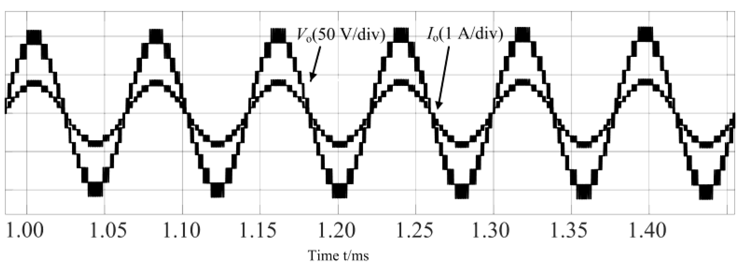
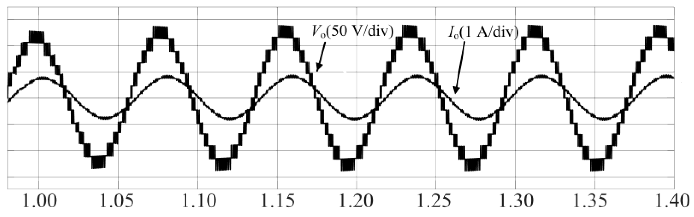
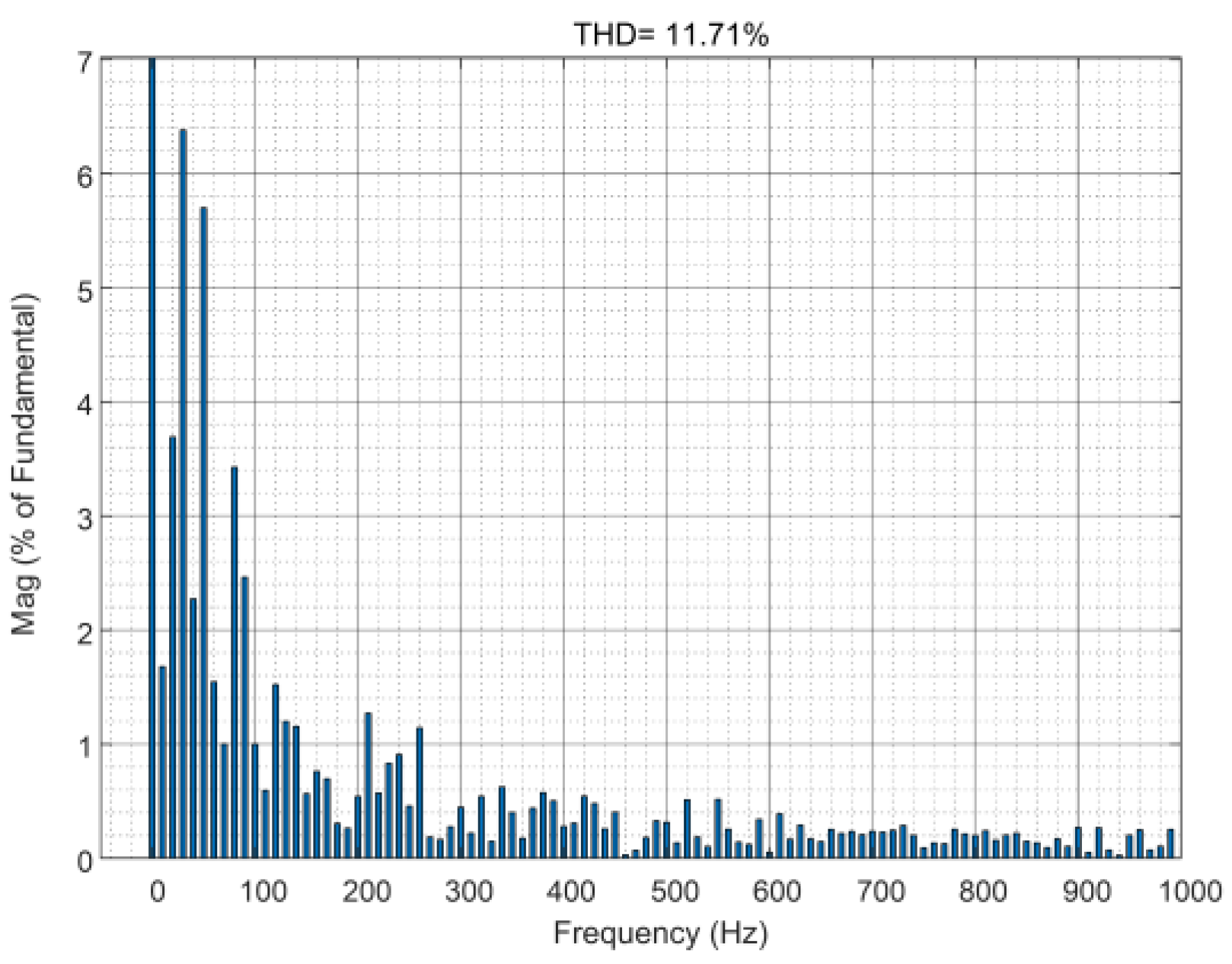
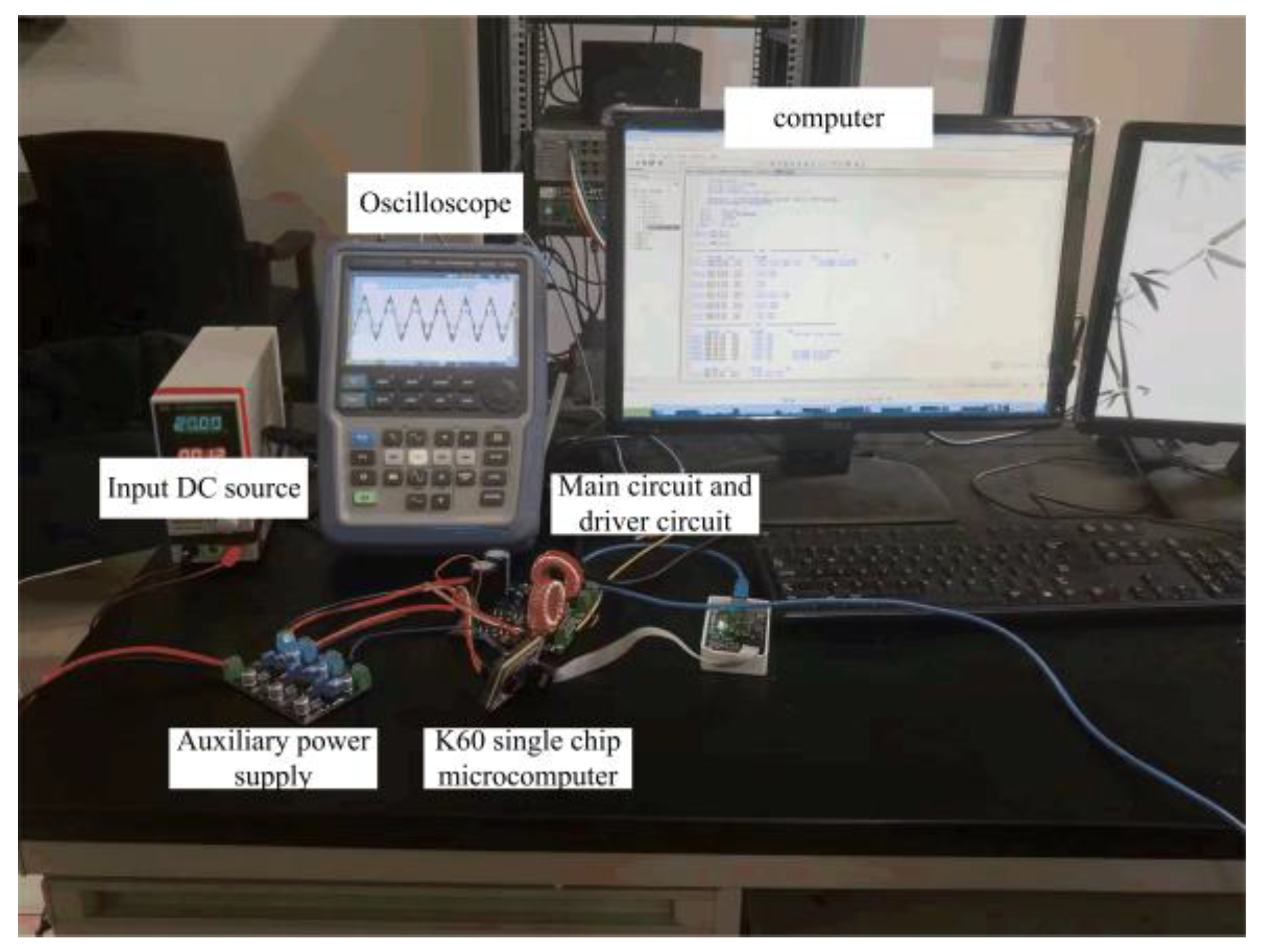
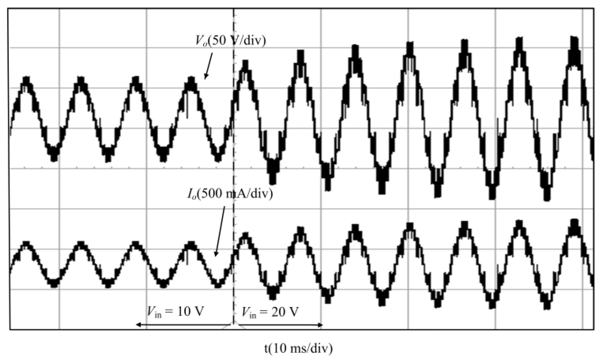
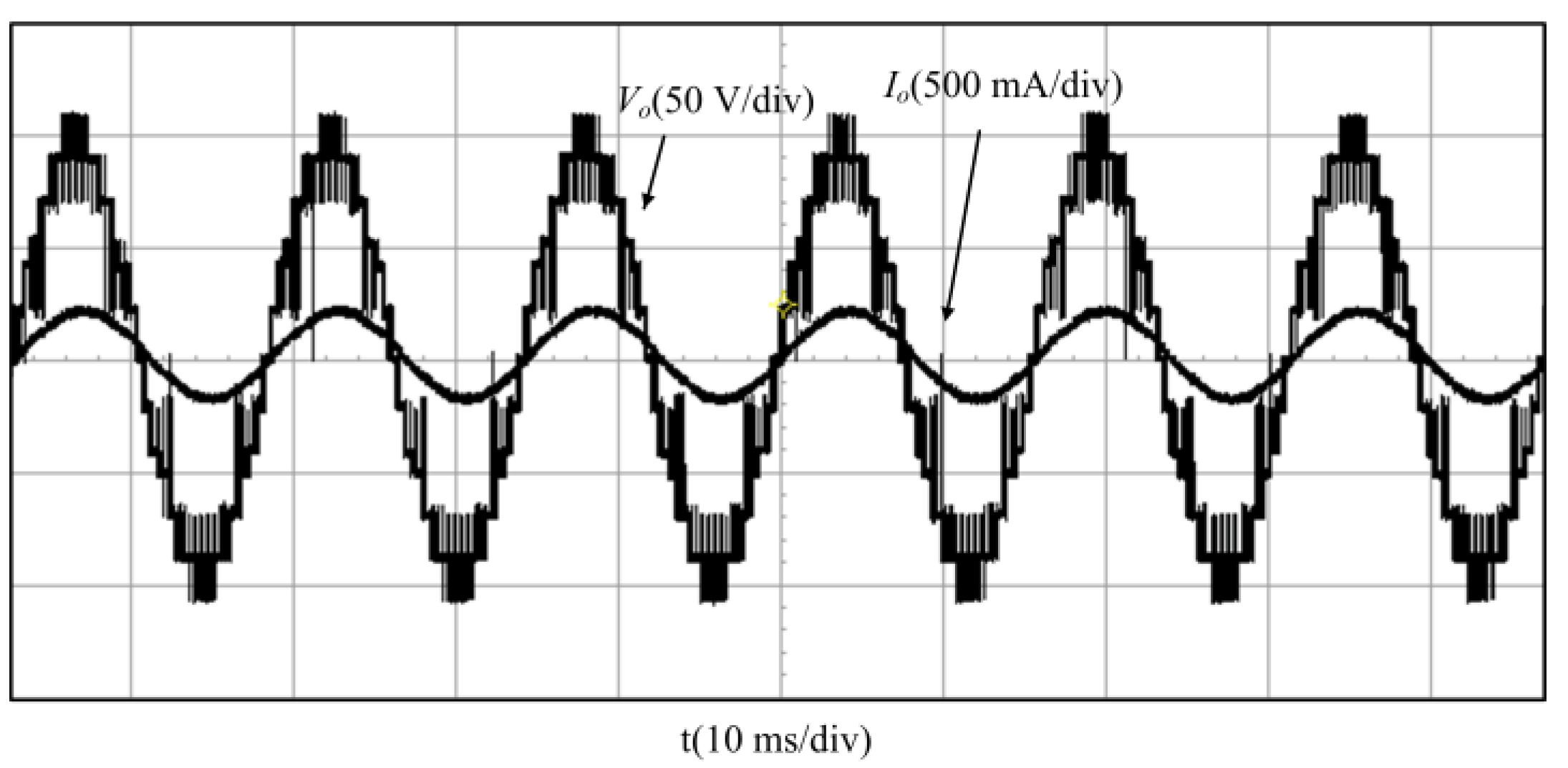
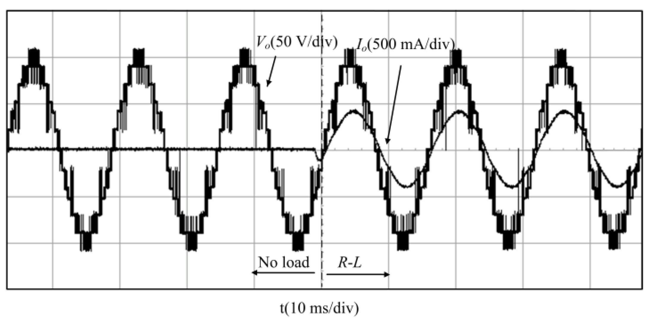
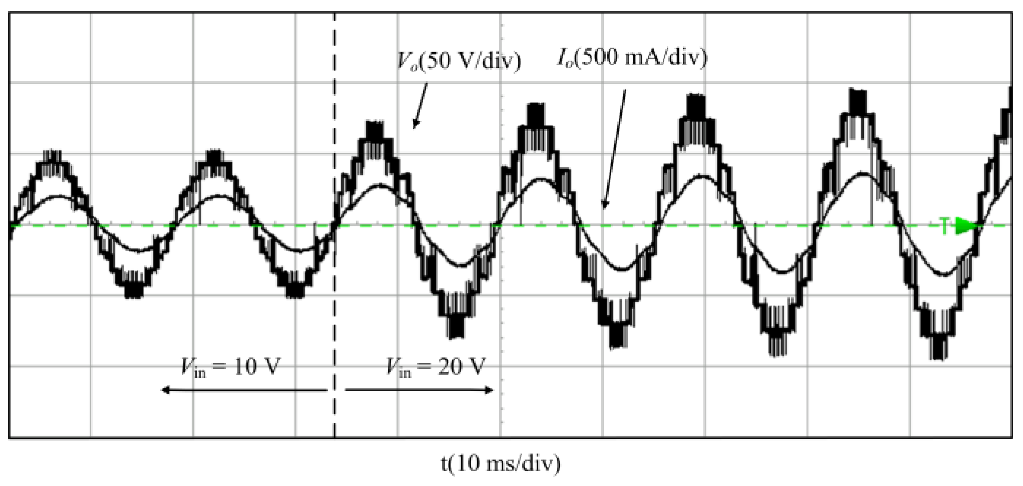
5.2. Experimental Validation

In order to further verify the correctness of the topology and its performance under steady-state and dynamic conditions, an experimental prototype was built, as shown in Figure 8.
To further verify the correctness of the topology, an experimental prototype is built. The main circuit is driven by the control signal generated by the K60 series microcontroller to control the turn-on and turn-off of each switch tube, so as to realize the output of the thirteen-level. The parameters are shown in Table 4.
According to the modulation method in Figure 4, the K60 single chip microcomputer drives the on–off of fourteen switching tubes in the main circuit with the generated logic signal, and obtains the driving signal waveform of each switching tube of the inverter, as shown in Figure 9. It can be seen from the figure that the switching frequency of each switch tube is consistent with the theoretical analysis and simulation of the modulation strategy, which verifies the correctness of the conduction sequence of the switch tube.
The voltage of the fourteen switch tubes S1S14 is shown in Figure 10. It can be seen that the MBV of S1S4 in the dual-capacitor base module is 20 V, 16 V, 18 V and 16 V, respectively. The MBV of S5S9 in the expansion module is 20 V, 52 V, 52 V and 44 V, respectively. In the half-bridge module, the S11, S12 and S13, S14 are 40 V and 44 V, respectively.
The current of fourteen switching tubes S1–S14 is shown in Figure 11. It can be seen that the maximum current of all switching tubes is within 5 A.
When the DC input voltage is 20 V, the output voltage and current waveform of the system with a pure resistive load are shown in Figure 12. As can be seen from the figure, the load current waveform is a stepped wave, consistent with the output voltage waveform. The peak output voltage is 120 V, which achieves a voltage gain of six times. Moreover, after stabilization, the standard thirteen-level step wave can be output, which further verifies the feasibility of the topology.
When the system power supply voltage Vin changes from 10 V to 20 V, the waveform diagram is shown in Figure 13. It can be seen that the inverter can react quickly and stabilize in the new state.
Under the group inductive load R = 100 Ω and L = 40 mH, the reactive power capacity of the proposed SC-MLI was evaluated with an inductive resistance load of 161 VA according to IEEE standard 1547 [31]. The power factor (PF) was 0.89, and the topological output voltage and current were shown in Figure 14. As can be seen in the figure, the output voltage is a standard thirteen-level step wave, and the load current waveform is a smooth sine wave, which lags behind the output voltage waveform, proving the capability of the topology to provide reactive power.
When the load changes from no-load to group load with R = 100 Ω and L = 40 mH, the experimental output waveform is shown in Figure 15.
It can be seen that the output voltage remains unchanged, and the load current changes with the load, indicating that the output voltage can remain stable when the load changes, and it has a good ability to adapt to load mutations. When the power supply voltage Vin changes from 10 V to 20 V, the waveform diagram is shown in Figure 16.
Under different output power, the efficiency of the proposed topology is shown in Figure 17. When the output power changes from 100 W to 500 W, the efficiency is always above 93%, and the highest is 95.7%. When the output power is less than 300 W, the efficiency is higher than 95%. When the input voltage of the inverter is 20 V and the output power is 200 W, the efficiency is 95.3%, higher than 94% and 92.3% in reference [27,29].

6. Conclusions

In this paper, an extensible thirteen-level SC-MLI is proposed to achieve higher output step wave and voltage gain with fewer devices. It has the advantages of fewer devices and automatic capacitor voltage balance, and can expand the topology by adding expansion modules as required. Compared with the existing topology, the proposed inverter has certain advantages in the number of components, MBV and TSV. Finally, an experimental prototype is used to verify the inverter. According to the experimental results, the proposed topology can output thirteen-level stepped waves stably, with self-balancing capacitor voltage and six-times voltage gain effect. Additionally, it can still work normally when the load changes, with excellent dynamic stability to meet the needs of inverter applications, at the same time, it has a high power conversion efficiency, the maximum value is more than 95%.

Author Contributions

Conceptualization, S.L., L.L., W.H. and N.D.; methodology, L.L. and Q.W.; formal analysis, L.L.; writing—original draft preparation, W.H. All authors have read and agreed to the published version of the manuscript.

Funding

This research was funded by National Natural Science Fund, grant number 51977072.

Institutional Review Board Statement

Not applicable.

Informed Consent Statement

Not applicable.

Data Availability Statement

Not applicable.

Conflicts of Interest

The authors declare no conflict of interest.

References

  1. Ye, Y.; Zhang, G.; Wang, X.; Yi, Y.; Cheng, K.W.E. Self-Balanced Switched-Capacitor Thirteen-Level Inverters with Reduced Capacitors Count. IEEE Trans. Ind. Electron. 2022, 69, 1070–1076. [Google Scholar] [CrossRef]
  2. Tayyab, M.; Sarwar, A.; Hussan, M.R.; Murshid, S.; Tariq, M.; Alamri, B. A novel voltage boosting switched-capacitor 19-level inverter with reduced component count. Int. J. Circuit Theory Appl. 2022, 50, 2128–2149. [Google Scholar] [CrossRef]
  3. Chen, S.; Ye, Y.; Hua, T.; Wang, X. Self-balanced switched-capacitor multilevel inverter with asymmetric double-wing structure. Int. J. Electr. Power Energy Syst. 2021, 133, 107295. [Google Scholar] [CrossRef]
  4. Zamiri, E.; Vosoughi, N.; Hosseini, S.H.; Barzegarkhoo, R.; Sabahi, M. A new cascaded switched-capacitor multilevel inverter based on improved series–parallel conversion with less number of components. IEEE Trans. Ind. Electron. 2016, 63, 3582–3594. [Google Scholar] [CrossRef]
  5. Zhang, X.; Wang, M.; Zhao, T.; Mao, W.; Hu, Y.; Cao, R. Topological comparison and analysis of medium-voltage and high-power direct-linked PV inverter. CES Trans. Electr. Mach. Syst. 2019, 3, 327–334. [Google Scholar] [CrossRef]
  6. Jena, K.; Kumar, D.; Janardhan, K.; Kumar, B.H.; Singh, A.R.; Nikolovski, S.; Bajaj, M. A Novel Three-Phase Switched-Capacitor Five-Level Multilevel Inverter with Reduced Components and Self-Balancing Ability. Appl. Sci. 2023, 13, 1713. [Google Scholar] [CrossRef]
  7. Wang, Y.; Wang, K.; Li, G.; Wu, F.; Wang, K.; Liang, J. Generalized switched-capacitor step-up multilevel inverter employing single DC source. CSEE J. Power Energy Syst. 2021, 8, 439–451. [Google Scholar]
  8. Ye, Y.; Chen, S.; Wang, X.; Cheng, K.W.E. Self-balanced 13-level inverter based on switched capacitor and hybrid PWM algorithm. IEEE Trans. Ind. Electron. 2020, 68, 4827–4837. [Google Scholar] [CrossRef]
  9. Zheng, X.; Yao, J.; Xu, Z.; Ioinovici, A. Multioutput Switched-Capacitor Multilevel Inverter with Intrinsic Elimination of the Photovoltaics Induced Leakage Current and High Boost Factor. IEEE Trans. Ind. Electron. 2023, 70, 5850–5861. [Google Scholar] [CrossRef]
  10. Liu, J.; Zhu, X.; Zeng, J. A Seven-Level Inverter with SelfBalancing and Low-Voltage Stress. IEEE J. Emerg. Sel. Top. Power Electron. 2020, 8, 685–696. [Google Scholar] [CrossRef]
  11. Wang, Y.; Ye, J.; Ku, R.; Shen, Y.; Li, G.; Liang, J. A modular switched-capacitor multilevel inverter featuring voltage gain ability. J. Power Electron. 2023, 23, 11–22. [Google Scholar] [CrossRef]
  12. Ye, Y.; Chen, S.; Hua, T. Novel switched capacitor seven-level inverter with low voltage stress. Proc. CSEE 2021, 41, 4628–4636. [Google Scholar]
  13. Khodaparast, A.; Hassani, M.J.; Azimi, E.; Adabi, M.E.; Adabi, J.; Pouresmaeil, E. Circuit configuration and modulation of a seven-level switched-capacitor inverter. IEEE Trans. Power Electron. 2020, 36, 7087–7096. [Google Scholar] [CrossRef]
  14. Bana, P.R.; Panda, K.P.; Padmanaban, S.; Panda, G. Extendable switched-capacitor multilevel inverter with reduced number of components and self-balancing capacitors. IEEE Trans. Ind. Appl. 2020, 57, 3154–3163. [Google Scholar] [CrossRef]
  15. Hosseinzadeh, M.A.; Sarebanzadeh, M.; Garcia, C.F.; Babaei, E.; Rodriguez, J.; Kennel, R. Reduced Multisource Switched-Capacitor Multilevel Inverter Topologies. IEEE Trans. Power Electron. 2022, 37, 14647–14666. [Google Scholar] [CrossRef]
  16. Wang, Y.; Yuan, Y.; Li, G.; Ye, Y.; Wang, K.; Liang, J. A T-type switched-capacitor multilevel inverter with low voltage stress and self-balancing. IEEE Trans. Circuits Syst. I Regul. Pap. 2021, 68, 2257–2270. [Google Scholar] [CrossRef]
  17. Panda, K.P.; Bana, P.R.; Panda, G. A switched-capacitor self-balanced high-gain multilevel inverter employing a single DC source. IEEE Trans. Circuits Syst. II Express Briefs 2020, 67, 3192–3196. [Google Scholar] [CrossRef]
  18. Zeng, J.; Lin, W.; Liu, J. Switched-capacitor-based active-neutral-point-clamped seven-level inverter with natural balance and boost ability. IEEE Access 2019, 7, 126889–126896. [Google Scholar] [CrossRef]
  19. Kim, K.-M.; Han, J.-K.; Moon, G.-W. A High Step-Up Switched-Capacitor 13-Level Inverter with Reduced Number of Switches. IEEE Trans. Power Electron. 2021, 36, 2505–2509. [Google Scholar] [CrossRef]
  20. Wang, Y.; Wang, C.; Wang, K.; Chen, T. Switched capacitor multilevel inverter with step-charging and self-balancing. J. Electr. Mach. Control 2021, 25, 90–101. [Google Scholar]
  21. Zhao, J.; Lei, W.; Lyu, G.; Qian, L. Multi-objective reliability optimization design of MMC based on sensitivity analysis. Power Electron. 2021, 55, 24–28. [Google Scholar]
  22. Wu, Z.; Xiao, L.; Yao, Z.; Qin, W. Double-grounded transformer-less buck-boost photovoltaic grid-connected inverter based on hysteresis current control. Proc. CSEE 2021, 41, 8097–8107. [Google Scholar]
  23. Yuya, N.; Hirotaka, K. A boost-type nine-level switched capacitor inverter. IEEE Trans. Power Electron. 2019, 34, 6522–6532. [Google Scholar]
  24. Siddique, M.D.; Mekhilef, S.; Shah, N.M.; Ali, J.S.M.; Blaabjerg, F. A new switched capacitor 7L inverter with triple voltage gain and low voltage stress. IEEE Trans. Circuits Syst. II Express Briefs 2020, 67, 1294–1298. [Google Scholar] [CrossRef]
  25. Ying, H.; You, F.; Lin, L.; Liu, C.; Pei, Z. High-frequency isolated bidirectional PSFB (B-PSFB) converter optimal design. Electr. Drive 2020, 50, 60–65. [Google Scholar]
  26. Barzegarkhoo, R.; Kojabadi, H.M.; Zamiry, E.; Vosoughi, N.; Chang, L. Generalized structure for a single phase switched-capacitor multilevel inverter using a new multiple DC link producer with reduced number of switches. IEEE Trans. Power Electron. 2016, 31, 5604–5617. [Google Scholar] [CrossRef]
  27. Peng, W.; Ni, Q.; Qiu, X.; Ye, Y. Seven-level inverter with selfbalanced switched-capacitor and its cascaded extension. IEEE Trans. Power Electron. 2019, 34, 889–896. [Google Scholar] [CrossRef]
  28. Ge, X.J.; Sun, Y.; Wang, Z.H.; Tang, C.S. A single-source switched-capacitor multilevel inverter for magnetic coupling wireless power transfer systems. Electr. Eng. 2019, 101, 1083–1094. [Google Scholar] [CrossRef]
  29. Li, Q.; Chen, J.; Jiang, D. Periodic variation in the effect of switching frequency on the harmonics of power electronic converters. Chin. J. Electr. Eng. 2020, 6, 35–45. [Google Scholar] [CrossRef]
  30. Lee, S.S. Single-stage switched-capacitor module (S3CM) topologyfor cascaded multilevel inverter. IEEE Trans. Power Electron. 2018, 33, 8204–8215. [Google Scholar] [CrossRef]
  31. IEEE Std. 1547-2018; IEEE Standard for Interconnection and Interoperability of Distributed Energy Resources with Associated Electric Power Systems Interfaces. IEEE: Piscataway, NJ, USA, 2018; pp. 1–138.
Figure 1. Main Circuit of Thirteen-level Inverter.
Electronics 12 02259 g001
Figure 2. Operation model of two parallel photovoltaic distributed power system, they should be listed as: (a) 0+; (b) 0; (c) Vdc; (d) 2Vdc; (e) 3Vdc; (f) 4Vdc; (g) 5Vdc; (h) 6Vdc.
Electronics 12 02259 g002
Figure 3. Topological expansion of inverter topology.
Electronics 12 02259 g003
Figure 4. The modulation principal diagram of inverter, they should be listed as: (a) carrier and modulation waveform; (b) original PWM waveform; (c) the control signal waveform of each switch; (d) target output waveform; (e) inverter switching algorithm.
Electronics 12 02259 g004
Figure 5. Inverter output voltage and current waveform under pure resistance load.
Electronics 12 02259 g005
Figure 6. Inverter output voltage and current waveform under group inductive load.
Electronics 12 02259 g006
Figure 7. Output voltage THD waveform.
Electronics 12 02259 g007
Figure 8. Experimental platform.
Electronics 12 02259 g008
Figure 9. Experimental waveform of switch tube driving signal, they should be listed as: (a) S1, S2, S3, S4; (b) S5, S6, S7, S8; (c) S9, S10, S11, S12; (d) S13, S14.
Electronics 12 02259 g009
Figure 10. Switching tube voltage waveform: (a) S1, S2, S3, S4; (b) S5, S6, S7, S8; (c) S9, S10, S11, S12; (d) S13, S14.
Electronics 12 02259 g010
Figure 11. Switch tube current waveform: (a) S1, S2, S3, S4, S5, S6; (b) S7, S8, S9, S10; (c) S11, S12, S13, S14.
Electronics 12 02259 g011
Figure 12. Inverter experimental output voltage and current waveform under pure resistance load.
Electronics 12 02259 g012
Figure 13. Dynamic waveform of output voltage change experiment under pure resistance load.
Electronics 12 02259 g013
Figure 14. Waveform of output voltage and load current under group inductive load.
Electronics 12 02259 g014
Figure 15. Dynamic waveform of load change experiment under group inductive load.
Electronics 12 02259 g015
Figure 16. Dynamic waveform of power supply voltage change experiment under inductive load.
Electronics 12 02259 g016
Figure 17. Efficiency at different power.
Electronics 12 02259 g017
Table 1. Charging and discharging state of capacitor in different switching modes (▲: Charge ▼: Discharge —: Lie Idle).
Output VoltageOn-Off Switch TubeC1C2C3
6VdcS1, S3, S7, S8, S9, S11, S14
5VdcS1, S2, S4, S7, S8, S9, S11, S14
4VdcS2, S4, S5, S7, S8, S9, S11, S14
3VdcS1, S3, S6, S7, S9, S10, S11, S14
2VdcS1, S2, S4, S7, S10, S11, S14
VdcS2, S4, S5, S7, S10, S11, S14
0+S2, S4, S5, S6, S9, S11, S13
0S2, S4, S5, S7, S10, S12, S14
VdcS, S4, S5, S6, S9, S12, S13
−2VdcS1, S2, S4, S6, S9, S12, S13
−3VdcS1, S3, S6, S7, S9, S10, S12, S13
−4VdcS2, S4, S5, S6, S8, S10, S12, S13
−5VdcS1, S2, S4, S6, S8, S10, S12, S13
−6VdcS1, S3, S6, S8, S10, S12, S13
Table 2. Equivalent Parameters in Six Working Modes.
jUoreq
00 4 r s
1Vdc E S R + 6 r s
22Vdc E S R + 6 r s
33Vdc 2 E S R + 6 r s
44Vdc 2 E S R + 7 r s
55Vdc 2 E S R + 7 r s
66Vdc 3 E S R + 7 r s
Table 3. Comparison of Seven Thirteen-Level Switched Capacitor.
TopologyNCapacitorNSwitchNSourceMBVTSV
[25]4142632
[26]5191548
[27]5341134
[28]083324
[29]4182332
[30]4162335
Proposed3141332
Table 4. Component Parameters of Experimental Prototype.
ComponentsSpecifications (Parameters)
ControllerMK60FX512
Switching TubeIRF3205
DiodeFR104, 1N5819
Capacitance2200 uF, 4700 uF
Resistance100 Ω
Inductance40 mH
Switching frequency2 kHz
Output frequency50 Hz
Disclaimer/Publisher’s Note: The statements, opinions and data contained in all publications are solely those of the individual author(s) and contributor(s) and not of MDPI and/or the editor(s). MDPI and/or the editor(s) disclaim responsibility for any injury to people or property resulting from any ideas, methods, instructions or products referred to in the content.

