
Performance Comparison of Silicon- and Gallium-Nitride-Based MOSFETs for a Power-Efficient, DC-to-DC Flyback Converter

 ,
,  ,
,  and
and
Abstract
:
1. Introduction
2. Methodology
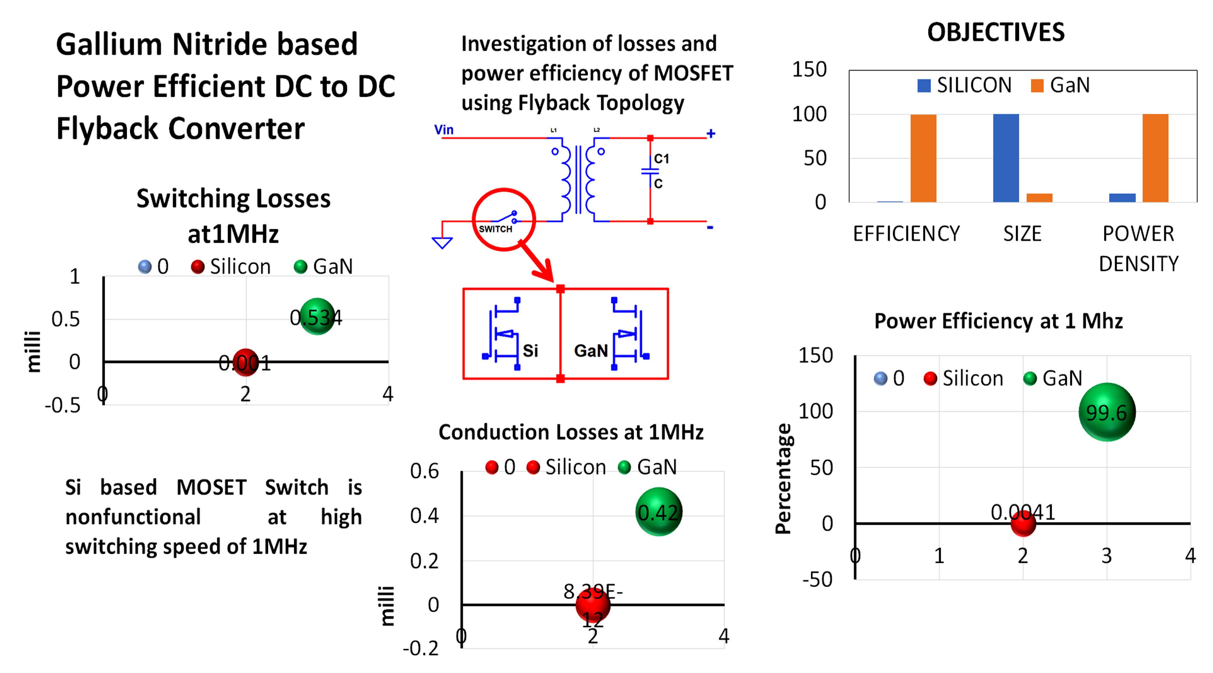
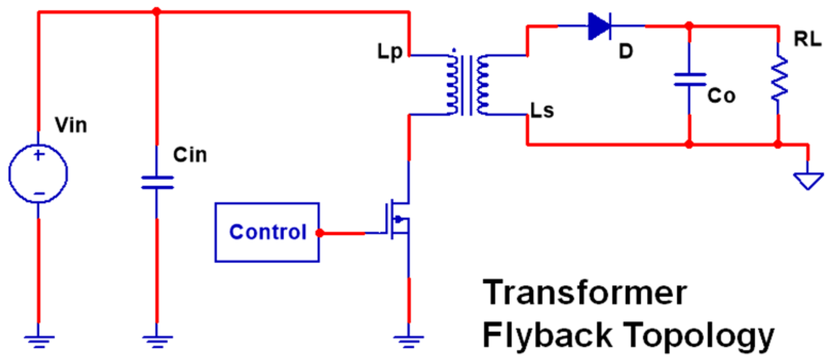
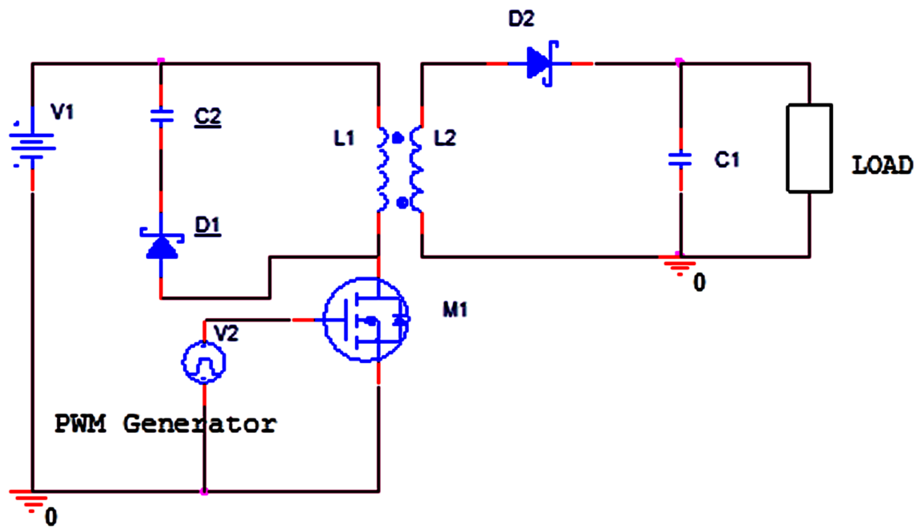
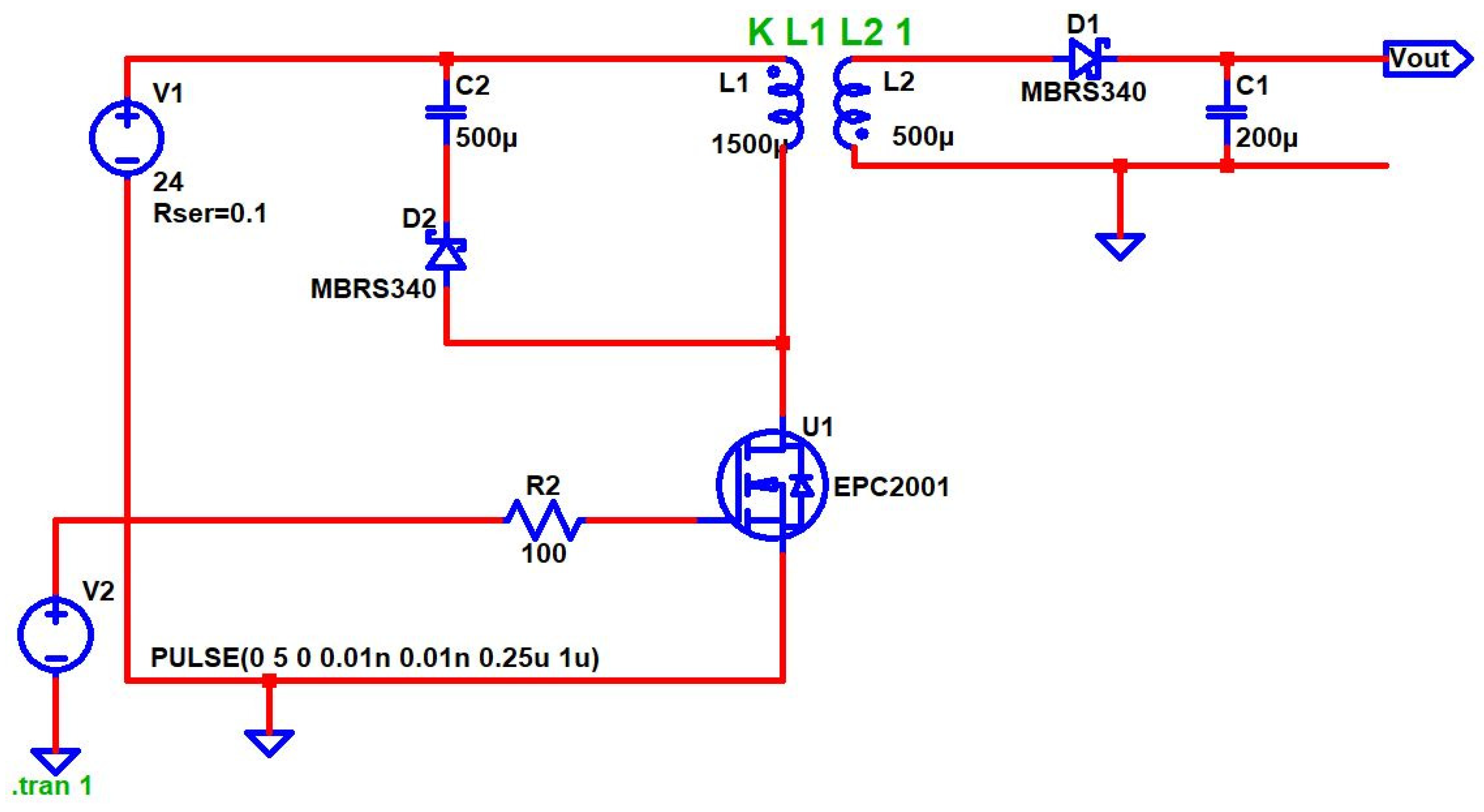
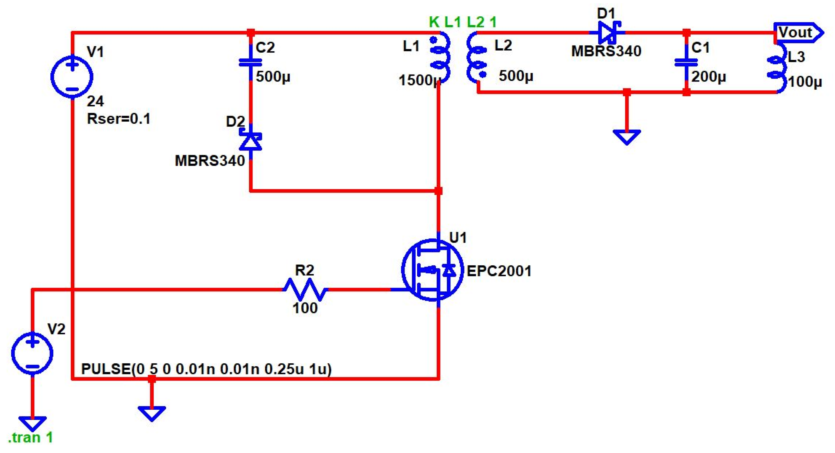
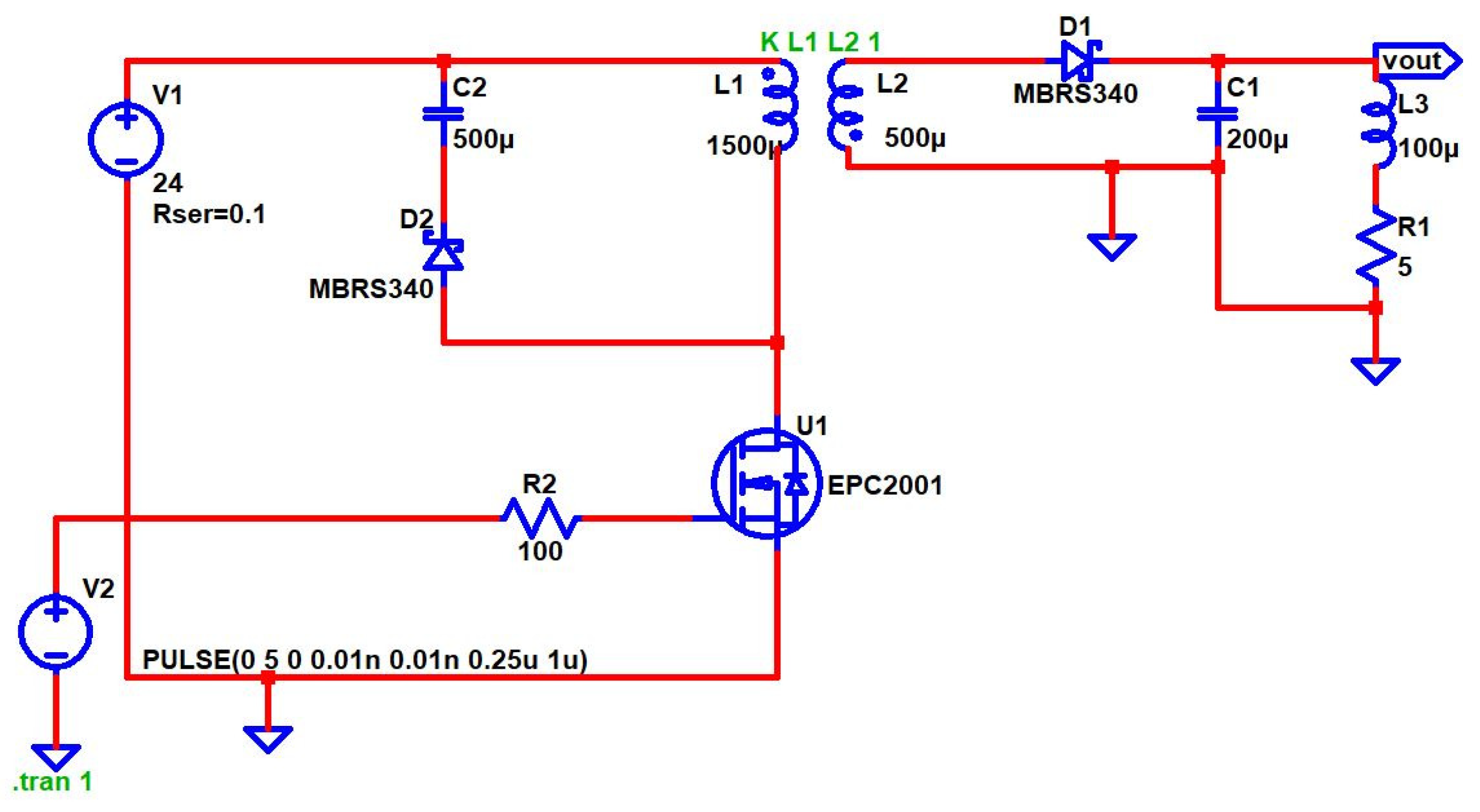
2.1. DC-to-DC Flyback Converter
2.2. Efficiency
2.3. Losses
2.3.1. MOSFET Conduction Losses
2.3.2. MOSFET Switching Losses
3. Results and Discussion
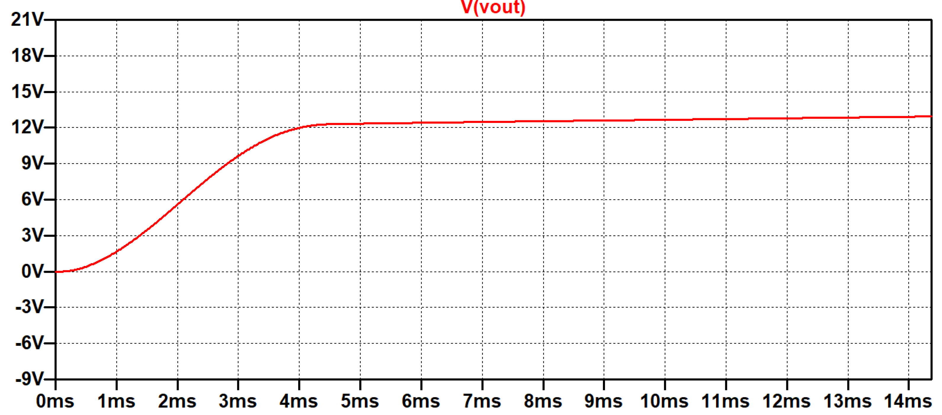
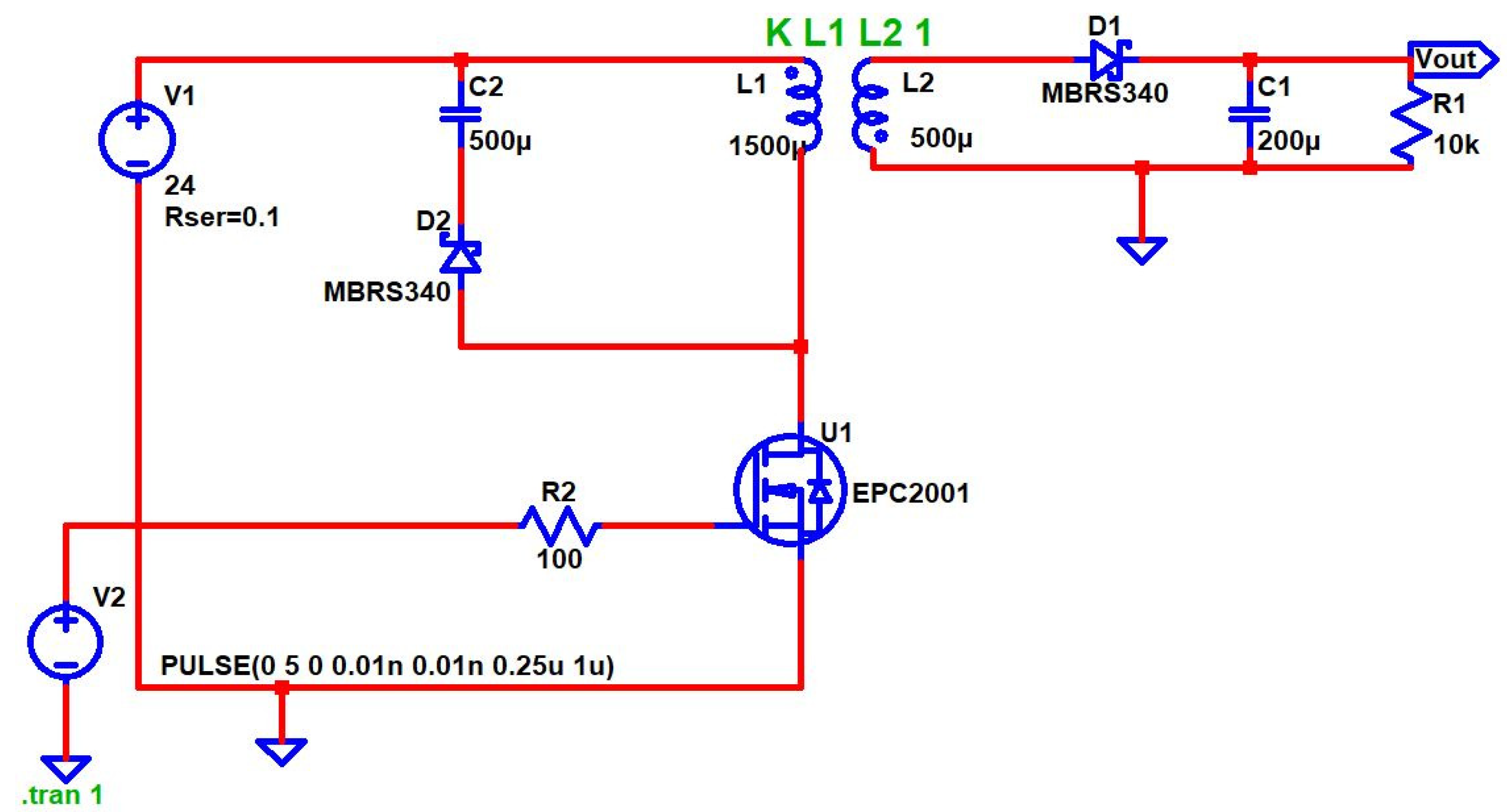
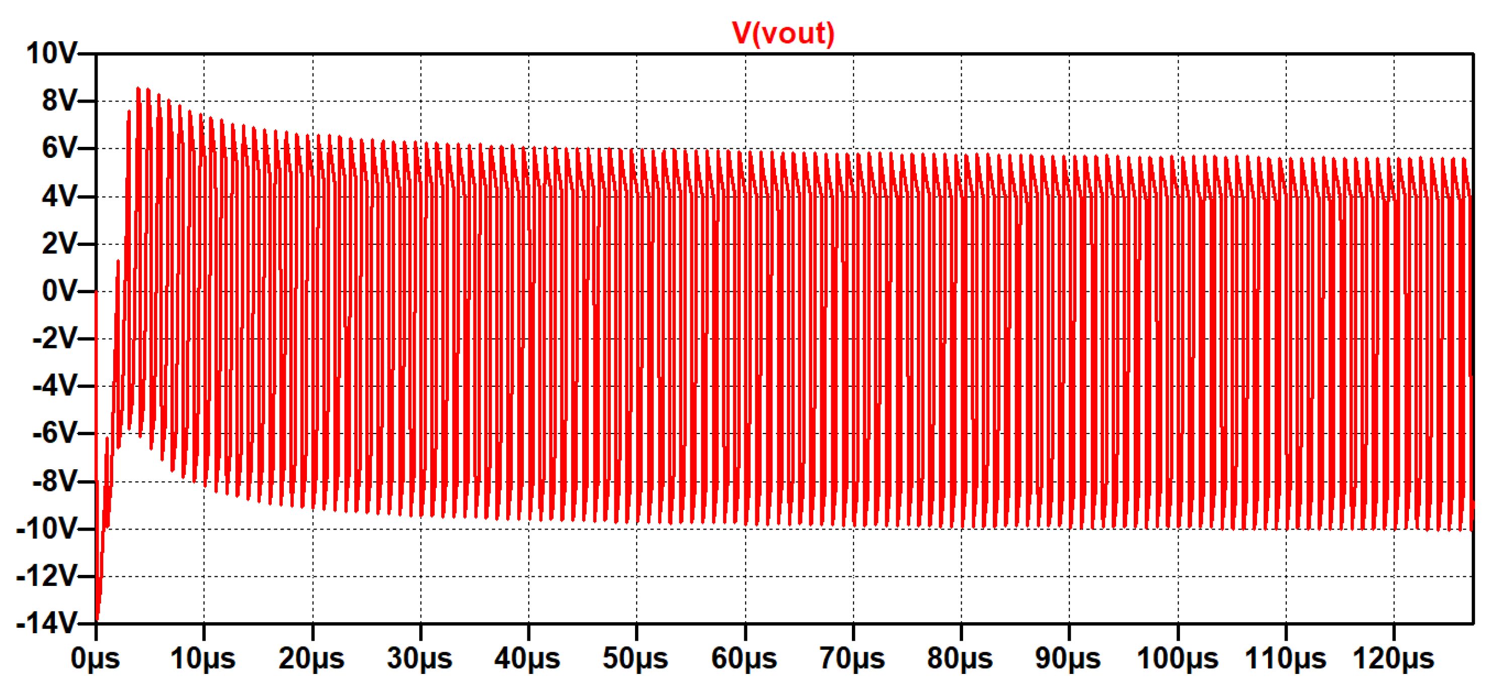
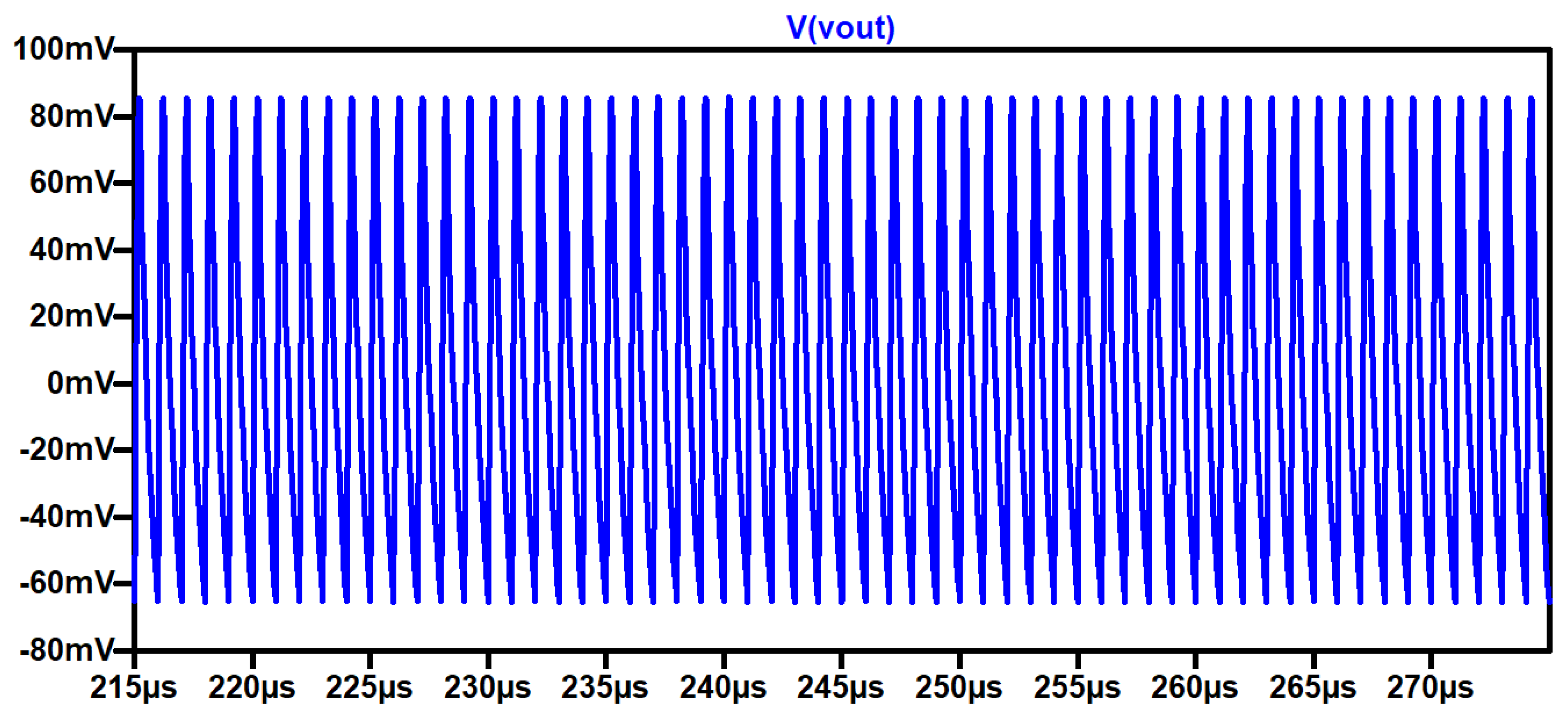
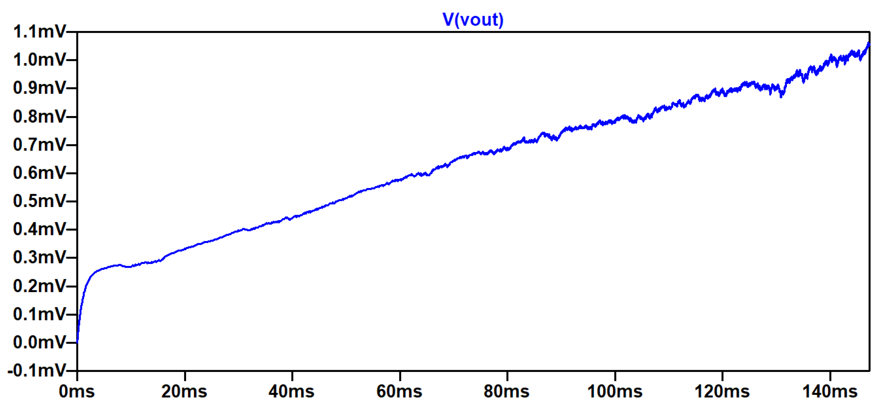
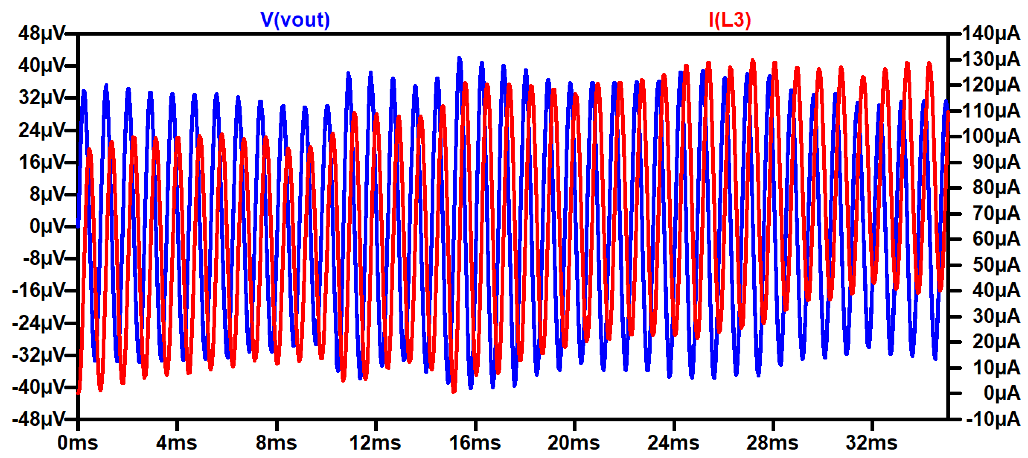
3.1. Open Circuit Configuration
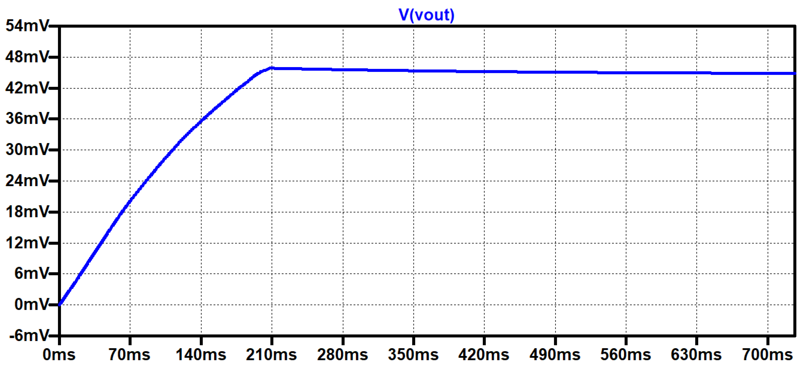
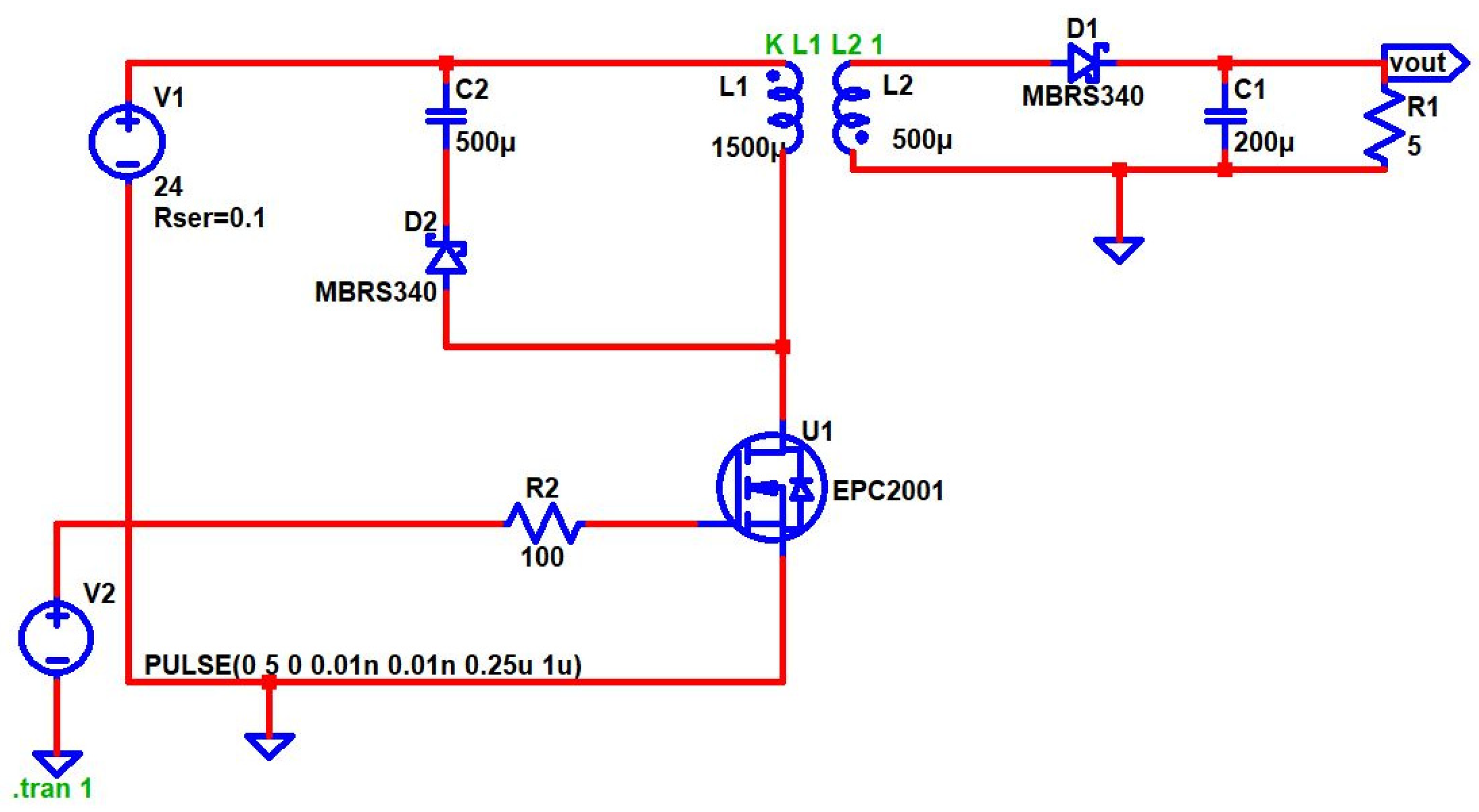
3.2. Resistive Load Configuration
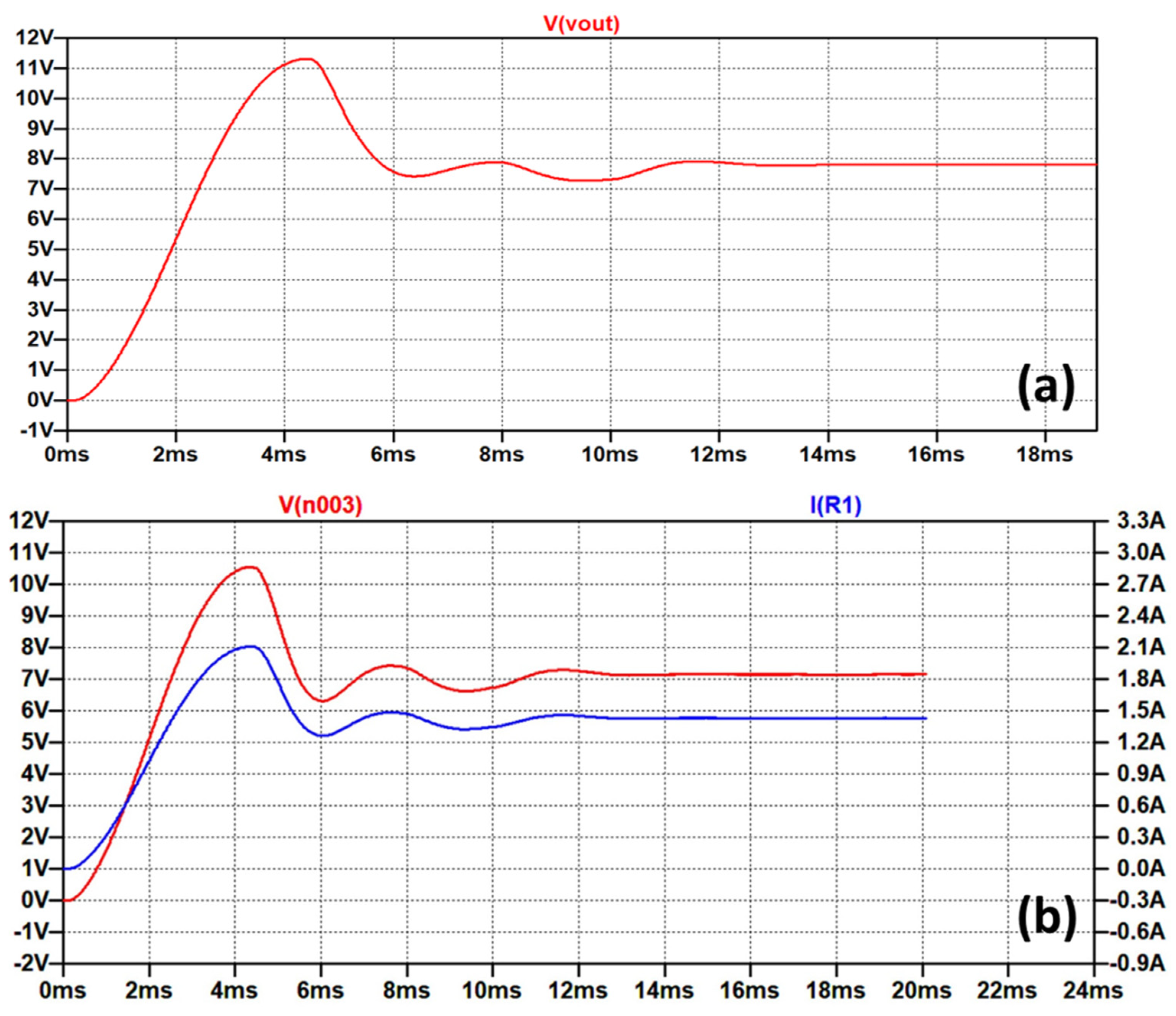
3.3. Inductive Load Configuration
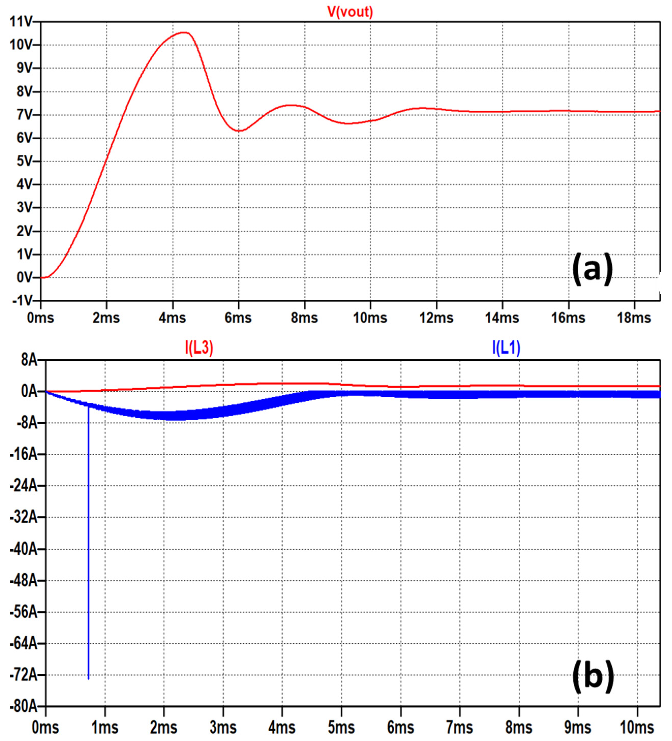
3.4. RLC Load Configuration
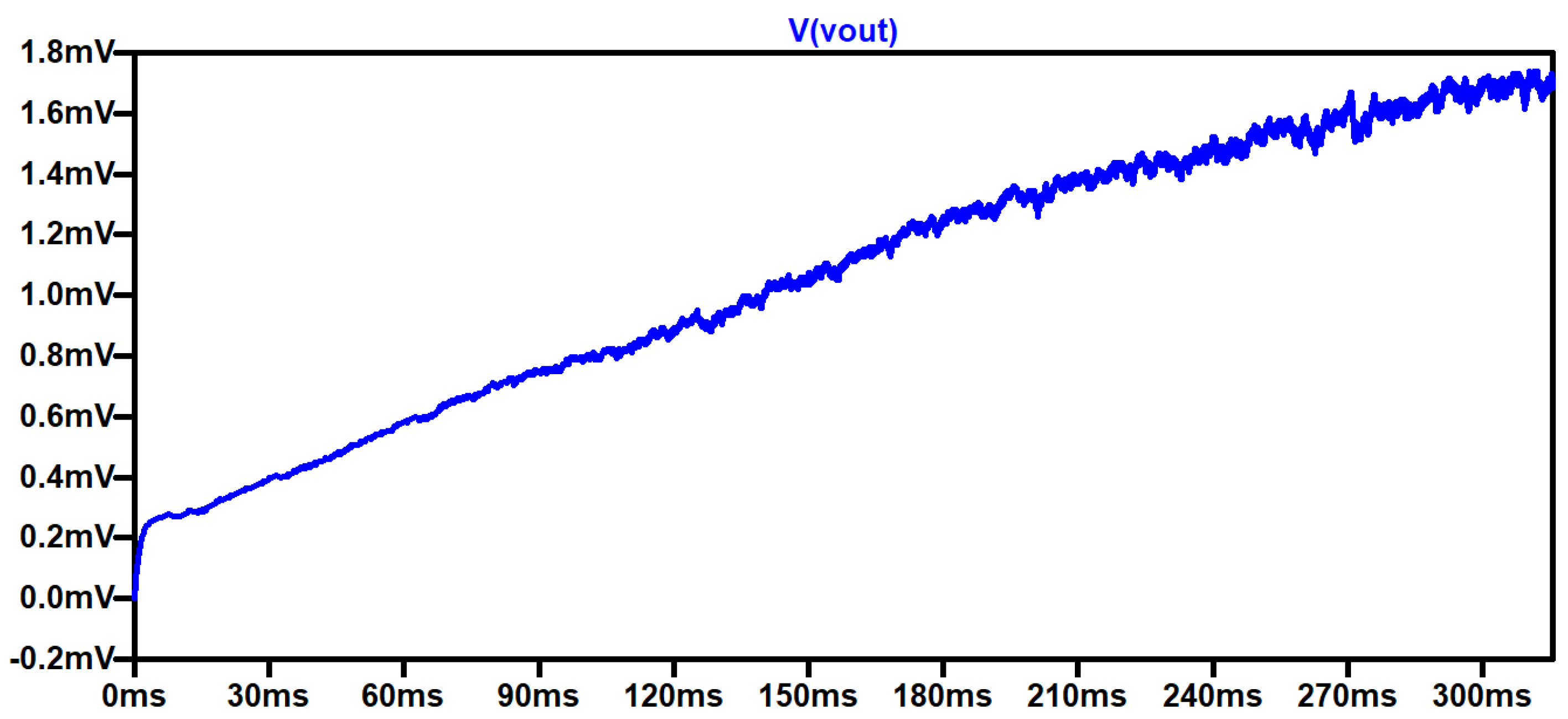
3.5. Comparative Analysis of Output Parameters
4. Conclusions
Author Contributions
Funding
Data Availability Statement
Acknowledgments
Conflicts of Interest
References
- Baliga, B.J. Evolution of MOS-bipolar power semiconductor technology. Proc. IEEE 1988, 76, 409–418. [Google Scholar] [CrossRef] [Green Version]
- Tajalli, A.; Meneghini, M.; Besendörfer, S.; Kabouche, R.; Abid, I.; Püsche, R.; Derluyn, J.; Degroote, S.; Germain, M.; Meissner, E.; et al. High breakdown voltage and low buffer trapping in superlattice gan-on-silicon heterostructures for high voltage applications. Materials 2020, 13, 4271. [Google Scholar] [CrossRef] [PubMed]
- Baliga, B.; Sears, A.; Barnicle, M.; Campbell, P.; Garwacki, W.; Walden, J. Gallium arsenide Schottky power rectifiers. IEEE Trans. Electron Devices 1985, 32, 1130–1134. [Google Scholar] [CrossRef]
- Baliga, B.J. Fundamentals of Power Semiconductor Devices; Springer: New York, NY, USA, 2008. [Google Scholar]
- Baliga, B.J. Advanced Power MOSFET Concepts; Springer Science & Business Media: New York, NY, USA, 2010. [Google Scholar]
- Yoder, M.N. Wide bandgap semiconductor materials and devices. IEEE Trans. Electron Devices 1996, 43, 1633–1636. [Google Scholar] [CrossRef]
- Denbaars, S.P. Gallium-nitride-based materials for blue to ultraviolet optoelectronics devices. Proc. IEEE 1997, 85, 1740–1749. [Google Scholar] [CrossRef]
- Baliga, B.J. Gallium nitride devices for power electronic applications. Semicond. Sci. Technol. 2013, 28, 074011. [Google Scholar] [CrossRef]
- Khoshzaman, S.; Hahn, I. A Performance Comparison of GaN FET and Silicon MOSFET. In Proceedings of the 2021 22nd IEEE International Conference on Industrial Technology (ICIT), Valencia, Spain, 10–12 March 2021; Volume 1, pp. 127–133. [Google Scholar]
- Khan, M.A.; Simin, G.; Pytel, S.G.; Monti, A.; Santi, E.; Hudgins, J.L. New developments in gallium nitride and the impact on power electronics. In Proceedings of the 2005 IEEE 36th Power Electronics Specialists Conference, Dresden, Germany, 16 June 2005; pp. 15–26. [Google Scholar]
- Meneghini, M.; De Santi, C.; Abid, I.; Buffolo, M.; Cioni, M.; Khadar, R.A.; Nela, L.; Zagni, N.; Chini, A.; Medjdoub, F.; et al. GaN-based power devices: Physics, reliability, and perspectives. J. Appl. Phys. 2021, 130, 181101. [Google Scholar] [CrossRef]
- Scott, M.J.; Fu, L.; Zhang, X.; Li, J.; Yao, C.; Sievers, M.; Wang, J. Merits of gallium nitride based power conversion. Semicond. Sci. Technol. 2013, 28, 074013. [Google Scholar] [CrossRef]
- Mishra, U.K.; Parikh, P.; Wu, Y.F. AlGaN/GaN HEMTs-an overview of device operation and applications. Proc. IEEE 2002, 90, 1022–1031. [Google Scholar] [CrossRef] [Green Version]
- Chu, R. GaN power switches on the rise: Demonstrated benefits and unrealized potentials. Appl. Phys. Lett. 2020, 116, 090502. [Google Scholar] [CrossRef]
- Reusch, D.; Strydom, J. Evaluation of gallium nitride transistors in high frequency resonant and soft-switching DC–DC converters. IEEE Trans. Power Electron. 2014, 30, 5151–5158. [Google Scholar] [CrossRef]
- Ballo, A.; Grasso, A.D.; Palumbo, G. A review of charge pump topologies for the power management of IoT nodes. Electronics 2019, 8, 480. [Google Scholar] [CrossRef] [Green Version]
- Ballo, A.; Bottaro, M.; Grasso, A.D.; Palumbo, G. Regulated charge pumps: A comparative study by means of verilog-AMS. Electronics 2020, 9, 998. [Google Scholar] [CrossRef]
- Meng, W.; Li, L.; Zhang, F.; Shu, J. Soft-switching Resonant Active Clamp Flyback Converter based-on GaN HEMTs for MHz High Step-up Applications. In Proceedings of the 2021 IEEE Workshop on Wide Bandgap Power Devices and Applications in Asia (WiPDA Asia), Wuhan, China, 25–27 August 2021; pp. 57–62. [Google Scholar]
- Dey, S.; Ray, M.B.; Soni, H.; Ghosh, R.; Shah, M. Comparison between Quasi-Resonant and Active Clamp Flyback topologies for GaN-based 65W Wall Charger Application. In Proceedings of the 2021 IEEE Applied Power Electronics Conference and Exposition (APEC), Phoenix, AZ, USA, 14–17 June 2021; pp. 1809–1814. [Google Scholar]
- Huang, D.; Gilham, D.; Feng, W.; Kong, P.; Fu, D.; Lee, F.C. High power density high efficiency dc/dc converter. In Proceedings of the 2011 IEEE Energy Conversion Congress and Exposition, Phoenix, AZ, USA, 17–22 September 2011; pp. 1392–1399. [Google Scholar]
- Wu, C.-C.; Liu, C.-Y.; Anand, S.; Chieng, W.-H.; Chang, E.-Y.; Sarkar, A. Comparisons on Different Innovative Cascode GaN HEMT E-Mode Power Modules and Their Efficiencies on the Flyback Converter. Energies 2021, 14, 5966. [Google Scholar] [CrossRef]
- Zhang, W.; Long, Y.; Zhang, Z.; Wang, F.; Tolbert, L.M.; Blalock, B.J.; Henning, S.; Wilson, C.; Dean, R. Evaluation and comparison of silicon and gallium nitride power transistors in LLC resonant converter. In Proceedings of the 2012 IEEE Energy Conversion Congress and Exposition (ECCE), Raleigh, NC, USA, 15–20 September 2012; pp. 1362–1366. [Google Scholar]
- Mortazavizadeh, S.A.; Palazzo, S.; Amendola, A.; De Santis, E.; Di Ruzza, D.; Panariello, G.; Sanseverino, A.; Velardi, F.; Busatto, G. High Frequency, High Efficiency, and High Power Density GaN-Based LLC Resonant Converter: State-of-the-Art and Perspectives. Appl. Sci. 2021, 11, 11350. [Google Scholar] [CrossRef]
- Costinett, D.; Nguyen, H.; Zane, R.; Maksimovic, D. GaN-FET based dual active bridge DC-DC converter. In Proceedings of the 2011 Twenty-Sixth Annual IEEE Applied Power Electronics Conference and Exposition (APEC), Fort Worth, TX, USA, 6–11 March 2011; pp. 1425–1432. [Google Scholar]
- Available online: https://epc-co.com/epc/Portals/0/epc/documents/datasheets/EPC2001C_datasheet (accessed on 15 February 2022).


| Property Name | Si | GaAs | SiC | 4HSiC | GaN | AlN | Diamond |
|---|---|---|---|---|---|---|---|
| Thermal expansion (×106 °C) | 2.6 | 5.9 | 4.7 | 4.2 | 5.6 | 4.5 | 0.08 |
| Density (g/cm3) | 2.328 | - | 3.210 | 3.211 | 6.095 | 3.255 | 3.515 |
| Melting point (Co) | 1420 | - | 3.210 | 2830 | 3530 | - | 4000 |
| Bandgap (eV) | 1.1 | 1.43 | 2.2 | 3.26 | 3.45 | 6.2 | 5.45 |
| Electron velocity (×107 s−1) | 1.0 | 1.0 | 2.2 | 2.0 | 2.2 | - | 2.7 |
| Breakdown (×105 Vcm−1) | 3 | 6 | 20 | 30 | >10 | - | 100 |
| Dielectric constant | 11.8 | 12.5 | 9.7 | 9.6 | 9 | 8.5 | 5.5 |
| Carrier mobility (cm2 N-s) electrons/holes | 1500/600 | 8500/400 | 1000/50 | 1140/50 | 1250/850 | - | 2200/1600 |
| BFOM (relative to Si) | 1.0 | 15.7 | 4.4 | - | 24.6 | - | 101 |
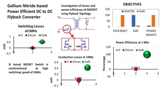
| S. No. | Parameters | Si Power MOSFET (W) (IXTK 200N10P) | GaN MOSFET (W) (EPC2001C) |
|---|---|---|---|
| 1 | Switching Loss at ON State (W) | 0 | 0.628 |
| 2 | Switching Loss at OFF State (W) | 0 | 1.885 |
| 3 | Total Switching Loss (W) | Not Working | 2.513 |
| 4 | Conduction Loss at ON State (W) | 0.000000000004 approx. zero | 0.420 × 10⁻³ |
| 6 | Total conduction loss at OFF state (W) | 0.000000000008 approx. zero | 0.840 × 10⁻³ |
| 7 | Inductive loss (W) | 1.074 | 39.2 m |
| 8 | Total loss (W) | maximum | 2.553 |
| 9 | Power-Efficiency of Converter (%) | 0.0041 | 99.6 |
Publisher’s Note: MDPI stays neutral with regard to jurisdictional claims in published maps and institutional affiliations. |
© 2022 by the authors. Licensee MDPI, Basel, Switzerland. This article is an open access article distributed under the terms and conditions of the Creative Commons Attribution (CC BY) license (https://creativecommons.org/licenses/by/4.0/).
Share and Cite
Ahmed, O.; Khan, Y.; Butt, M.A.; Kazanskiy, N.L.; Khonina, S.N. Performance Comparison of Silicon- and Gallium-Nitride-Based MOSFETs for a Power-Efficient, DC-to-DC Flyback Converter. Electronics 2022, 11, 1222. https://doi.org/10.3390/electronics11081222
Ahmed O, Khan Y, Butt MA, Kazanskiy NL, Khonina SN. Performance Comparison of Silicon- and Gallium-Nitride-Based MOSFETs for a Power-Efficient, DC-to-DC Flyback Converter. Electronics. 2022; 11(8):1222. https://doi.org/10.3390/electronics11081222
Chicago/Turabian StyleAhmed, Osama, Yousuf Khan, Muhammad A. Butt, Nikolay L. Kazanskiy, and Svetlana N. Khonina. 2022. "Performance Comparison of Silicon- and Gallium-Nitride-Based MOSFETs for a Power-Efficient, DC-to-DC Flyback Converter" Electronics 11, no. 8: 1222. https://doi.org/10.3390/electronics11081222