Article

Low Power Consumption Gate-Tunable WSe2/SnSe2 van der Waals Tunnel Field-Effect Transistor

Department of Electrical Engineering, Chosun University, 375, Seosuk-dong, Dong-gu, Gwangju 501-759, Korea
*
Author to whom correspondence should be addressed.
Electronics 2022, 11(5), 833; https://doi.org/10.3390/electronics11050833
Submission received: 4 February 2022 / Revised: 4 March 2022 / Accepted: 4 March 2022 / Published: 7 March 2022
(This article belongs to the Section Semiconductor Devices)

Abstract

:
Two-dimensional (2D) transition-metal dichalcogenides (TMDCs) have attracted attention as promising next-generation electronic devices and sensors. In this study, we fabricated a novel nanoelectronic device based on a black-phosphorus-gated WSe2/SnSe2 van der Waals (vdW) tunnel field-effect transistor (TFET), where hexagonal boron nitride (h-BN) was used as the gate insulator. We performed morphological, electrical, and optoelectronic characterizations. The p-WSe2/n-SnSe2 heterostructure-based TFET exhibited p-type behavior with a good dependence on the gate voltage. The TFET device showed a trend toward negative differential resistance (NDR) originating from band-to-band tunneling, which can be tuned by applying a gate voltage. The optoelectronic performance of the TFET device was low, with a maximum photoresponsivity of 11 mA W−1, owing to the large device length. The results obtained herein promote the integration of black phosphorus into low-energy-consumption 2D vdW TFETs.

1. Introduction

Two-dimensional (2D) van der Waals (vdW) heterostructures have been widely studied for the development of nanoelectronics. Transition-metal dichalcogenides (TMDCs) have attracted significant attention for several applications, such as memory and logic circuits [1,2], photocatalytic water splitting devices [3], field-effect transistors [4,5], tunneling transistors [6], bipolar junction transistors [7], ferroelectric field-effect transistor (FE) transistors [8,9], ferromagnetic transistors [10], and sensors [11,12,13]. Transition-metal dichalcogenides have suitable energy bandgaps for electronic and optoelectronic devices. In particular, tungsten diselenide (WSe2), which is an intrinsic semiconductor [14] with an energy band gap of 1.2 eV for its bulk form (up to 1.65 eV for the monolayer) [15,16], and tin diselenide (SnSe2), which is degenerately n-doped with an energy bandgap of 1.0 eV [17], are appropriate for such applications. Two-dimensional black phosphorus (BP) is promising for low-power-consumption electronic devices [18]. BP has an infrared band gap energy of ~0.3 eV (bulk), which is tunable to ~2 eV (monolayer) by reducing the layer thickness [19] and goes down to 0.05 eV by electric field modulation [20]. Hexagonal boron nitride (h-BN) is a dielectric material with a high band gap of ~6 eV, and thus, it is useful as an insulator layer for MOS devices and as a dielectric for device shielding [21].
In this study, we fabricated a novel low-power-consumption, gate-tunable WSe2/SnSe2 vdW tunnel field-effect transistor (TFET). We used BP as the gate contact and h-BN as the insulator layer between the gate and channel. We carried out morphological characterizations and investigated the electrical and optoelectronic properties of the gated WSe2/SnSe2 TFET, where the device showed a trend toward negative differential resistance (NDR) owing to the band-to-band tunneling (BTBT) phenomenon. We were able to control the tunneling effect by varying the applied gate voltage.

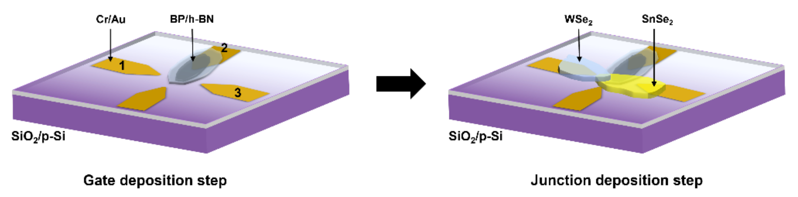
2. Materials and Methods

BP, hexagonal boron nitride (h-BN), tungsten diselenide (WSe2), and tin diselenide (SnSe2) were purchased from HQ Graphene; X-ray Diffraction (XRD) data of the 2D materials are shown in Figure S1. The fabrication process is shown schematically in Figure 1. First, chromium/gold (10/50 nm) were deposited by thermal evaporation onto a 300-nm SiO2/silicon substrate, followed by the successive deposition of few-layered BP (gate contact) and h-BN (gate insulator) through the mechanical exfoliation technique using flexible polydimethylsiloxane (PDMS). Subsequently, few-layered n-type SnSe2 and p-type WSe2 were successively deposited using the same technique. The device was not annealed to prevent SnSe2 degradation. The morphological properties were observed using scanning electron microscopy (SEM; Hitachi TM-1000; Japan) and atomic force microscopy (AFM; inVia Reflex). For electrical and optoelectronic characterizations, we used a HP 4155A semiconductor parameter analyzer. Optoelectronic properties were evaluated using a laser source with power values varying from 0.015 to 3.193 μW, wavelength, and spot diameter of 532 and 20 μm, respectively.

3. Results and Discussion

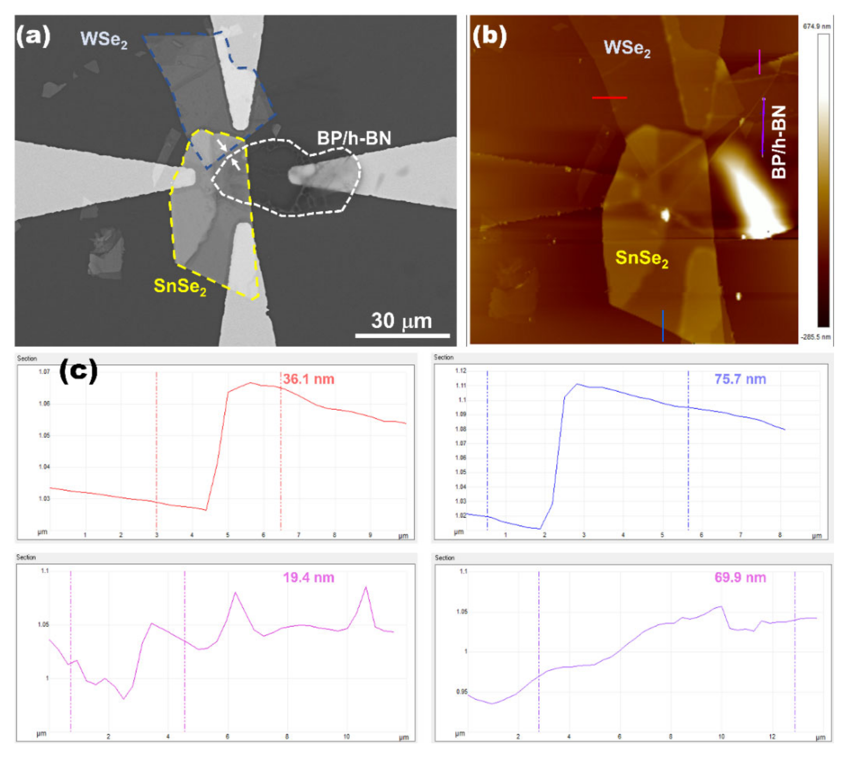
3.1. Morphological Characterization

Figure 2a shows an SEM image of the gated TFET, showing multilayered WSe2, SnSe2, and h-BN/BP in blue, yellow, and white dotted lines, respectively. The length of the device was 30 μm. The h-BN/BP junction and WSe2 did not intersect in the vertical direction, as observed in the figure; thus, the thickness of the insulator was roughly estimated to be 2 μm based on the distance between the edges of multilayered BP and WSe2 (white arrows in Figure 3a). Figure 2b shows the corresponding AFM image, where the red, blue, pink, and purple lines indicate the cross-sections of the WSe2, SnSe2, h-BN, and h-BN/BP junctions, respectively. The thicknesses of the top WSe2, SnSe2, h-BN, and h-BN/BP junctions were determined by topographic analysis at 36, 76, 20, and 70 nm, respectively, as shown in Figure 2c. Thus, the thickness of multilayered BP was determined to be 50 nm.

3.2. Energy Band Diagram

Figure 3a,c shows the energy band diagrams of the device in the vertical direction, i.e., Figure 3a,c corresponds to the p-WSe2/h-BN/BP and n-SnSe2/h-BN/BP heterostructures, respectively. The energy band gap for SnSe2 is ~1.0 eV, its electron affinity is 4.85 eV, and its work function is 5.0 eV [22]. For WSe2, the energy band gap and electron affinity are 1.3 and 3.5 eV, respectively [23]. In both configurations, the heterostructures are in accumulation mode: accumulation of holes and electrons at the p-WSe2/h-BN and the n-SnSe2/h-BN interface, respectively. Figure 3b,d shows the corresponding current–voltage (I–V) curves. When the absolute value of the voltage was increased to 1 V, the current increased, which was probably due to the tunneling effect in the vertical direction because the insulator layer was very thin (20 nm).

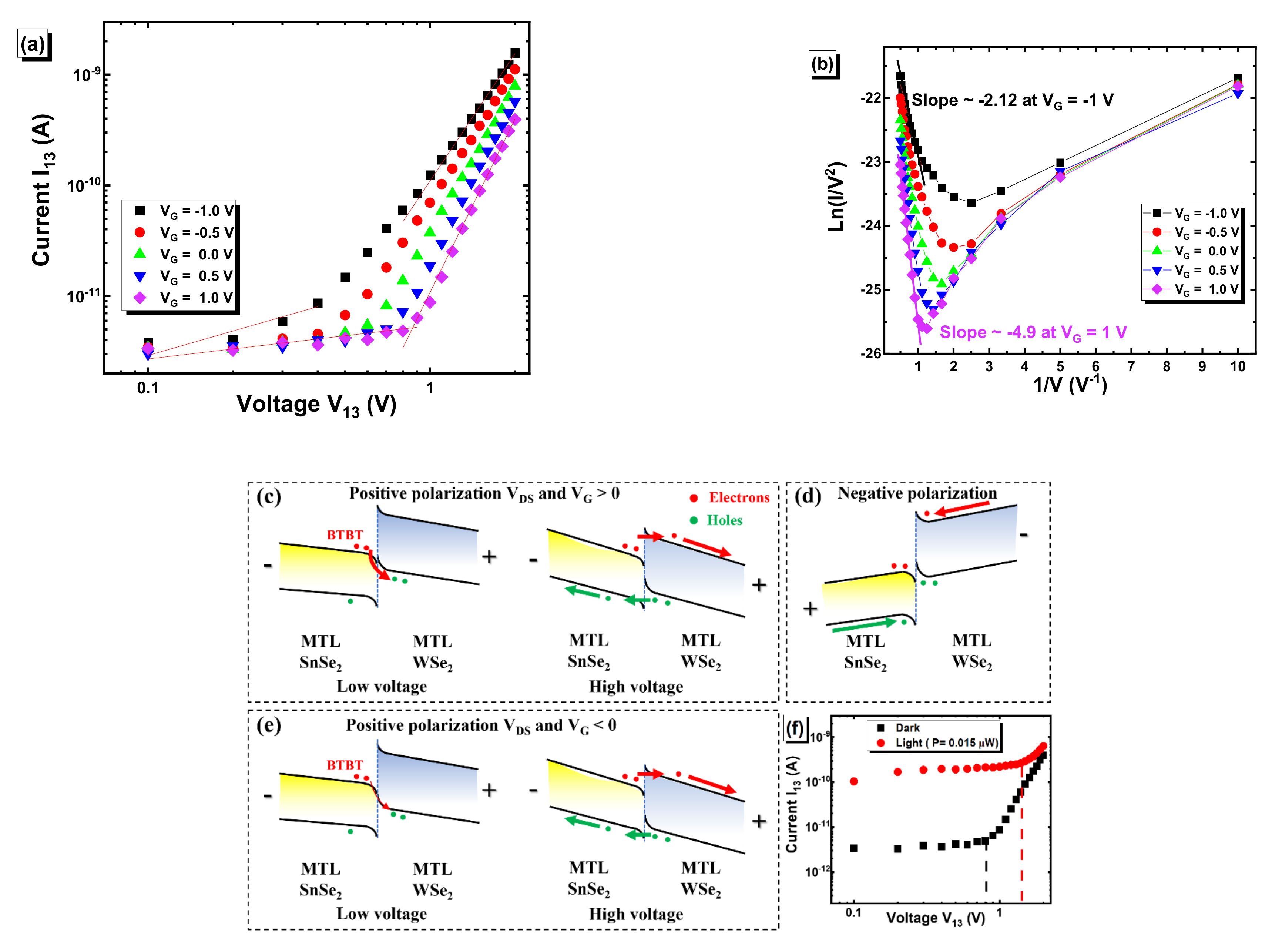
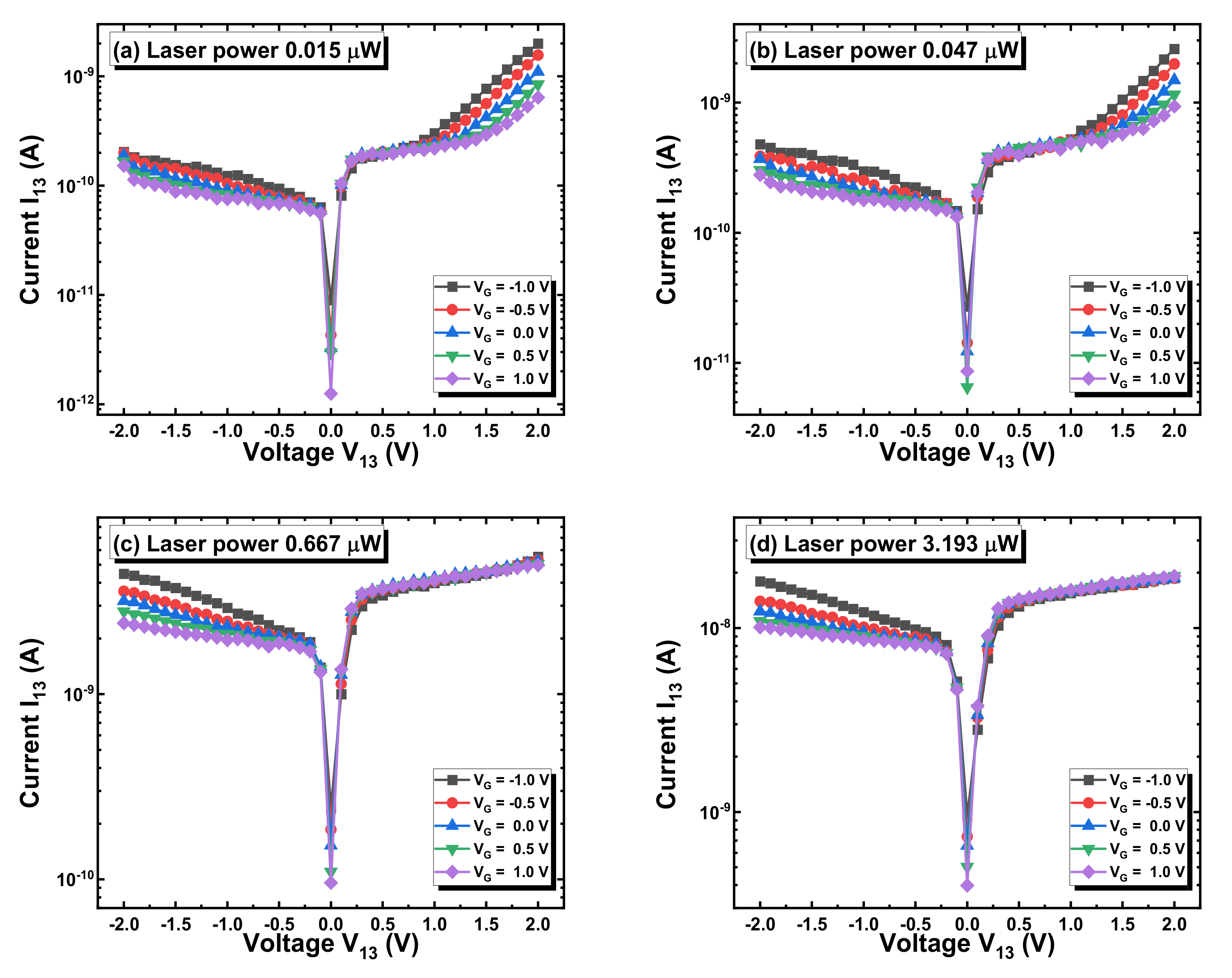
3.3. Electrical and Optoelectronic Characterizations

Figure 4a,b shows the transfer characteristics of the BP-gated p-WSe2/n-SnSe2 heterostructure when SnSe2 and WSe2 were used, respectively. Both configurations exhibited p-type behavior, where the current increased with decreasing gate voltage. When grounding multilayered WSe2, the device demonstrated good gate voltage dependence in both cases with an ION/IOFF ratio of 20 at a polarization voltage of 2 V (Figure 4b).
To investigate the current transport in the BP-gated p-Wse2/n-SnSe2 heterostructure, we drew an energy band diagram in the longitudinal direction, as shown in Figure 5a. At equilibrium, the p-Wse2/n-SnSe2 heterostructure showed a broken (type-III) band alignment. Figure 5b,c shows the I–V characteristics of the p-Wse2/n-SnSe2 heterostructure when SnSe2 and Wse2, respectively, were used as common contacts at different gate voltages. The gate voltage had a lower effect when Wse2 was used as a common contact because BP and Wse2 had no intersection, as shown in Figure 2. As shown in Figure 5b, a change in the current curve was observed around a polarization and gate voltage of 1 V. Similar behavior was observed in a p-Si back-gated Wse2/SnSe2 heterostructure, which was explained by the trend toward NDR [24]. When the gate voltage was decreased from 1 to −1 V, the I–V curves shifted to lower voltages.
Figure 6a shows the log-scale current at different gate voltages. Two distinct linear regimes can be observed in the forward current region. The two observed regimes can be modeled using direct tunneling (DT) and Fowler–Nordheim tunneling (FNT), according to the following equations [25]:
I D T V = A q 2 V d s m φ B h 2 d e x p 4 π d m * φ B h
I FNT V = A q 3 m V d s 2 8 π h φ B d 2 m * e x p 8 π d φ B 3 / 2 2 m * 3 h q V d s
where A , φ B , q , m , m * , d , and h are the effective contact area, barrier height, electron charge, free-electron mass, effective electron mass, barrier width, and Planck’s constant, respectively. Ln (I/V2) versus 1/V is plotted in Figure 6b; according to Equations (1) and (2), the curve should show linear and logarithmic regimes for FNT and DT, respectively. From the same figure, DT occurs at a low voltage and FNT dominates at a high voltage with a linear negative slope.
DT occurred at a low voltage in the positive gate voltage and forward regime (Figure 6c). However, when the polarization voltage increases to higher values, a change from broken (type-III) to staggered (type-II) can occur. Therefore, the BTBT phenomenon is weakened, and Fowler–Nordheim tunneling dominates. The inverse polarization (Figure 6d) revealed a diode-like band structure with electron and hole energy barriers at the p-Wse2/n-SnSe2 interface, which is the origin of the low reverse current. When a negative gate voltage was applied between BP and SnSe2, the valence and conduction bands of SnSe2 increased, and the BTBT phenomenon was weakened at a low polarization voltage. However, at higher polarization voltage values (Figure 6e), the FNT current was enhanced, which can explain the current shift to higher values observed in Figure 5b when a negative gate voltage was applied. Figure 6f shows the I–V curves of the positively polarized p-Wse2/n-SnSe2 heterostructure in dark and under a light excitation of 0.015 μW; the light enhanced the current and caused a shift to higher voltage values owing to the enhancement of the DT current.
Finally, the optoelectronic properties of the heterostructures were investigated. Figure 7a–d shows the I–V characteristics at different values of the gate voltage and laser power. When the laser power was increased, the current increased because of photogenerated carriers (electrons in the conduction bands and holes in the valence bands).
The photoresponsivity was deduced according to the equation R λ = I p h / P = I l i g h t I d a r k / P , where I p h represents the photocurrent and P is the laser power. Figure 8a,b corresponds to the photoresponsivity of the p-WSe2/n-SnSe2 heterostructure-based TFET at negative and positive polarization voltages, respectively. The variation in the photoresponsivity was more homogeneous at a polarization voltage of −2 V (Figure 8a) and it increased to ~11 mA W−1 at a gate voltage of −1 V and laser power of 0.015 μW. Moreover, it decreased when the laser power is increased, a phenomenon that is commonly observed in TMDC-based photodetectors [26], which is attributed to the trapping effect.
The optoelectronic properties of WSe2/SnSe2 heterojunctions have not been investigated in detail. As seen in Table 1, the photoresponsivity of our device was larger than the value reported by Chauhan et al. [27] but lower than those reported by Xue et al. [28] and Sun et al. [29]. The low photoresponsivity was due to the long channel length of the device (30 μm). It should be noted that both the photoresponsivity and ION/IOFF ratio can be improved using multiple interdigitated electrodes and by shortening the channel length.

4. Conclusions

We fabricated a BP-gated WSe2/SnSe2 vdW TFET. We carried out morphological characterizations and investigated the electrical and optoelectronic properties of the p-WSe2/n-SnSe2 heterostructure in the vertical and longitudinal directions. The TFET device showed p-type behavior with good dependence on the gate voltage and a trend toward NDR originating from BTBT phenomenon. We succeeded in controlling the tunneling effect by varying the applied gate voltage. The maximum photoresponsivity of the device was ~11 mA W−1, which was slightly small because of the long channel length of our device (30 μm). We believe that the results presented herein will promote the fabrication of tunneling effect transistors based only on two-dimensional materials. In future research, we believe that the optimization of the device dimensions will significantly improve its electrical and optoelectronic performance.

Supplementary Materials

The following supporting information can be downloaded at: https://www.mdpi.com/article/10.3390/electronics11050833/s1, Figure S1: X-ray diffraction (XRD) images of black phosphorus (BP), hexagonal boron nitride (h-BN), tungsten diselenide (WSe2), and tin diselenide (SnSe2).

Author Contributions

Methodology, C.W.; writing—original draft preparation, A.A.; writing—review and editing, P.-J.K. All authors have read and agreed to the published version of the manuscript.

Funding

This work was supported by the Brain Pool Program through the National Research Foundation of Korea (NRF), funded by the Ministry of Science and ICT (NRF-2019H1D3A1A01102658). This study was supported by a research fund from Chosun University, 2021.

Data Availability Statement

Data is available from the corresponding author upon the request.

Conflicts of Interest

The authors declare no conflict of interest.

References

  1. Tong, L.; Peng, Z.; Lin, R.; Li, Z.; Wang, Y.; Huang, X.; Xue, K.-H.; Xu, H.; Liu, F.; Xia, H.; et al. 2D materials–based homogeneous transistor-memory architecture for neuromorphic hardware. Science 2021, 373, 1353–1358. [Google Scholar] [CrossRef] [PubMed]
  2. Yin, L.; Cheng, R.; Wang, Z.; Wang, F.; Sendeku, M.G.; Wen, Y.; Zhan, X.; He, J. Two-Dimensional Unipolar Memristors with Logic and Memory Functions. Nano Lett. 2020, 20, 4144–4152. [Google Scholar] [CrossRef]
  3. Shanker, G.S.; Biswas, A.; Ogale, S.B. 2D materials and their heterostructures for photocatalytic water splitting and conversion of CO2 to value chemicals and fuels. J. Phys. Energy 2021, 3, 022003. [Google Scholar] [CrossRef]
  4. Conti, S.; Pimpolari, L.; Calabrese, G.; Worsley, R.; Majee, S.; Polyushkin, D.K.; Paur, M.; Pace, S.; Keum, D.H.; Fabbri, F.; et al. Low-voltage 2D materials-based printed field-effect transistors for integrated digital and analog electronics on paper. Nat. Commun. 2020, 11, 3566. [Google Scholar] [CrossRef] [PubMed]
  5. Abderrahmane, A.; Ko, P.J.; Thu, T.V.; Ishizawa, S.; Takamura, T.; Sandhu, A. High photosensitivity few-layered MoSe2 back-gated field-effect phototransistors. Nanotechnology 2014, 25, 365202. [Google Scholar] [CrossRef] [PubMed]
  6. Das, S.; Prakash, A.; Salazar, R.; Appenzeller, J. Toward low-power electronics: Tunneling phenomena in transition metal dichalcogenides. ACS Nano 2014, 8, 1681–1689. [Google Scholar] [CrossRef]
  7. Zhu, W.; Low, T.; Wang, H.; Ye, P.; Duan, X. Nanoscale electronic devices based on transition metal dichalcogenides. 2D Mater. 2019, 6, 032004. [Google Scholar] [CrossRef]
  8. Luo, Z.-D.; Xia, X.; Yang, M.-M.; Wilson, N.R.; Gruverman, A.; Alexe, M. Artificial optoelectronic synapses based on ferroelectric field-effect enabled 2D transition metal dichalcogenide memristive transistors. ACS Nano 2019, 14, 746–754. [Google Scholar] [CrossRef]
  9. Kim, J.Y.; Choi, M.-J.; Jang, H.W. Ferroelectric field effect transistors: Progress and perspective. APL Mater. 2021, 9, 021102. [Google Scholar] [CrossRef]
  10. Xie, L.; Cui, X. Manipulating spin-polarized photocurrents in 2D transition metal dichalcogenides. Proc. Natl. Acad. Sci. USA 2016, 113, 3746–3750. [Google Scholar] [CrossRef] [Green Version]
  11. Wang, L.; Xu, D.; Jiang, L.; Gao, J.; Tang, Z.; Xu, Y.; Chen, X.; Zhang, H. Transition Metal Dichalcogenides for Sensing and Oncotherapy: Status, Challenges, and Perspective. Adv. Funct. Mater. 2021, 31, 2004408. [Google Scholar] [CrossRef]
  12. Urbanos, F.J.; Gullace, S.; Samorì, P. Field-Effect Transistors Based Ion Sensors: Ultrasensitive Mercury (II) Detection via Healing of MoS2 Defects. Nanoscale 2021, 13, 19682–19689. [Google Scholar] [CrossRef] [PubMed]
  13. Shu, Y.; Yang, Y.; Gao, Q. Interlayer engineering of two-dimensional transition-metal disulfides for electrochemical and optical sensing applications. FlatChem 2021, 27, 100242. [Google Scholar] [CrossRef]
  14. Jin, Z.; Li, X.; Mullen, J.T.; Kim, K.W. Intrinsic transport properties of electrons and holes in monolayer transition-metal dichalcogenides. Phys. Rev. B 2014, 90, 045422. [Google Scholar] [CrossRef] [Green Version]
  15. Yu, P.; Lin, J.; Sun, L.; Le, Q.L.; Yu, X.; Gao, G.; Hsu, C.-H.; Wu, D.; Chang, T.-R.; Zeng, Q.; et al. Metal-Semiconductor Phase-Transition in WSe2(1-x) Te2x Monolayer. Adv. Mater. 2017, 29, 1603991. [Google Scholar] [CrossRef] [PubMed]
  16. Choi, W.; Choudhary, N.; Han, G.H.; Park, J.; Akinwande, D.; Lee, Y.H. Recent development of two-dimensional transition metal dichalcogenides and their applications. Mater. Today 2017, 20, 116–130. [Google Scholar] [CrossRef]
  17. Narro-Rios, J.S.; Ramachandran, M.; Martínez-Escobar, D.; Sánchez-Juárez, A. Ultrasonic spray pyrolysis deposition of SnSe and SnSe2 using a single spray solution. J. Semicond. 2013, 34, 013001. [Google Scholar] [CrossRef]
  18. Abderrahmane, A.; Woo, C.; Ko, P.J. Black Phosphorus/Molybdenum Diselenide Heterojunction-Based Photodetector. J. Electron. Mater. 2021, 50, 5713–5720. [Google Scholar] [CrossRef]
  19. Li, J.; Luo, H.; Zhai, B.; Lu, R.; Guo, Z.; Zhang, H.; Liu, Y. Black phosphorus: A two-dimension saturable absorption material for mid-infrared Q-switched and mode-locked fiber lasers. Sci. Rep. 2016, 6, 30361. [Google Scholar] [CrossRef] [Green Version]
  20. Zong, X.; Hu, H.; Ouyang, G.; Wang, J.; Shi, R.; Zhang, L.; Zeng, Q.; Zhu, C.; Chen, S.; Cheng, C.; et al. Black phosphorus-based van der Waals heterostructures for mid-infrared light-emission applications. Light Sci. Appl. 2020, 9, 114. [Google Scholar] [CrossRef]
  21. Li, A.; Chen, Q.; Wang, P.; Gan, Y.; Qi, T.; Wang, P.; Tang, F.; Wu, J.Z.; Chen, R.; Zhang, L.; et al. Ultrahigh-sensitive broadband photodetectors based on dielectric shielded MoTe2/Graphene/SnS2 p–g–n junctions. Adv. Mater. 2019, 31, e1805656. [Google Scholar] [CrossRef] [PubMed]
  22. Mukhokosi, E.P.; Roul, B.; Krupanidhi, S.B.; Nanda, K.K. Toward a fast and highly responsive SnSe2-based photodiode by exploiting the mobility of the counter semiconductor. ACS Appl. Mater. Interfaces 2019, 11, 6184–6194. [Google Scholar] [CrossRef] [PubMed]
  23. Schulman, D.S.; Arnold, A.J.; Das, S. Contact engineering for 2D materials and devices. Chem. Soc. Rev. 2018, 47, 3037–3058. [Google Scholar] [CrossRef] [PubMed]
  24. Yan, X.; Liu, C.; Li, C.; Bao, W.; Ding, S.; Zhang, D.W.; Zhou, P. Tunable SnSe2/WSe2 heterostructure tunneling field effect transistor. Small 2017, 13, 1701478. [Google Scholar] [CrossRef]
  25. Vu, Q.A.; Lee, J.H.; Nguyen, V.L.; Shin, Y.S.; Lim, S.C.; Lee, K.; Heo, J.; Park, S.; Kim, K.; Lee, Y.H.; et al. Tuning carrier tunneling in van der Waals heterostructures for ultrahigh detectivity. Nano Lett. 2017, 17, 453–459. [Google Scholar] [CrossRef]
  26. Furchi, M.M.; Polyushkin, D.; Pospischil, A.; Mueller, T. Mechanisms of photoconductivity in atomically thin MoS2. Nano Lett. 2014, 14, 6165–6170. [Google Scholar] [CrossRef] [Green Version]
  27. Chauhan, P.; Patel, A.B.; Solanki, G.K.; Machhi, H.K.; Sumesh, C.K.; Soni, S.S.; Patel, V.; Pathak, V.M. Ultrasonically exfoliated nanocrystal-based Z-scheme SnSe2/WSe2 heterojunction for a superior electrochemical photoresponse. J. Phys. Chem. C 2021, 125, 14729–14740. [Google Scholar] [CrossRef]
  28. Xue, H.; Dai, Y.; Kim, W.; Wang, Y.; Bai, X.; Qi, M.; Halonen, K.; Lipsanen, H.; Sun, Z. High photoresponsivity and broadband photodetection with a band-engineered WSe 2/SnSe 2 heterostructure. Nanoscale 2019, 11, 3240–3247. [Google Scholar] [CrossRef] [Green Version]
  29. Sun, Y.; Hu, R.; An, C.; Ma, X.; Zhang, J.; Liu, J. Visible to near-infrared photodetector based on SnSe2/WSe2 heterojunction with potential application in artificial visual neuron. Nanotechnology 2021, 32, 475206. [Google Scholar] [CrossRef]
Figure 1. Schematic representation of the fabricated WSe2/SnSe2 van der Waals heterostructure-based gated tunnel field-effect transistor.
Electronics 11 00833 g001
Figure 2. (a) SEM image and (b) AFM image of the BP-gated WSe2/SnSe2 van der Waals heterostructure. (c) Corresponding topographic analysis of WSe2, SnSe2, h-BN, and h-BN/BP junction.
Electronics 11 00833 g002
Figure 3. Energy band diagram of (a) p-WSe2/h-BN/BP and (c) n-SnSe2/h-BN/BP vdW heterostructures. I–V curves in vertical directions for (b) p-WSe2/h-BN/BP and (d) n-SnSe2/h-BN/BP vdW heterostructures.
Electronics 11 00833 g003
Figure 4. Gate voltage dependence of the current in BP-gated p-WSe2/n-SnSe2 heterostructure with (a) common SnSe2 and (b) common Wse2.
Electronics 11 00833 g004
Figure 5. (a) Energy band diagram of p-WSe2/ n-SnSe2 heterostructure in the longitudinal direction. I–V curves in longitudinal directions when (b) SnSe2 and (c) Wse2 are used as common contact.
Electronics 11 00833 g005
Figure 6. (a) Log current scale in the forward region and its corresponding (b) ln (I/V2)–1/V curve, energy band diagrams of p-WSe2/n-SnSe2 heterostructure, (c) (VDS > 0 and VG > 0), (d) (VDS < 0 and VG > 0), (e) (VDS > 0 and VG < 0), and (f) I–V curves of p-WSe2/n-SnSe2 heterostructure in dark and under light excitation.
Electronics 11 00833 g006
Figure 7. I–V curves in the longitudinal direction when SnSe2 was used as the common contact at different values of gate voltage and at a laser power value of (a) 0.015, (b) 0.047, (c) 0.667, and (d) 3.193 μW.
Electronics 11 00833 g007
Figure 8. Gate voltage and laser power dependence of the photoresponsivity in p-WSe2/n-SnSe2 heterostructure-based TFET at (a) negative and (b) positive polarization voltages.
Electronics 11 00833 g008
Table 1. Comparison of figures-of-merit for photodetectors based on WSe2/ SnSe2 heterojunction.
StructureSpectral RangeRλ (mAW−1)ION/IOFF RatioReference
BP-gated WSe2/SnSe2532 nm1120This work
WSe2/SnSe2532 nm1.03N/A[27]
WSe2/SnSe2532 nmN/A106[24]
WSe2/SnSe2532 nm588 × 103~104[28]
WSe2/SnSe2700 nm450~103 to ~104[29]
Publisher’s Note: MDPI stays neutral with regard to jurisdictional claims in published maps and institutional affiliations.

