Article

Noise Immunity-Enhanced Capacitance Readout Circuit for Human Interaction Detection in Human Body Communication Systems

1
School of Electrical and Electronics Engineering, Chung-Ang University, Seoul 06974, Korea
2
Electronics and Telecommunications Research Institute, Daejeon 34129, Korea
*
Author to whom correspondence should be addressed.
Electronics 2022, 11(4), 577; https://doi.org/10.3390/electronics11040577
Submission received: 21 January 2022 / Revised: 9 February 2022 / Accepted: 11 February 2022 / Published: 14 February 2022
(This article belongs to the Topic Wireless Sensor Networks)

Abstract

:
Recent healthcare systems based on human body communication (HBC) require human interaction sensors. Due to the conductive properties of the human body, capacitive sensors are most widely known and are applied to many electronic gadgets for communication. Capacitance fluctuations due to the fact of human interaction are typically converted to voltage levels using some analog circuits, and then analog-to-digital converters (ADCs) are used to convert analog voltages into digital codes for further processing. However, signals detected by human touch naturally contain large noise, and an active analog filter that consumes a lot of power is required. In addition, the inclusion of ADCs causes the system to use a large area and amount of power. The proposed structure adopts a digital-based moving average filter (MAF) that can effectively operate as a low-pass filter (LPF) instead of a large-area and high-power consumption analog filter. In addition, the proposed ∆C detection algorithm can distinguish between human interaction and object interaction. As a result, two individual digital signals of touch/release and movement can be generated, and the type and strength of the touch can be effectively expressed without the help of an ADC. The prototype chip of the proposed capacitive sensing circuit was fabricated with commercial 65 nm CMOS process technology, and its functionality was fully verified through testing and measurement. The prototype core occupies an active area of 0.0067 mm2, consumes 7.5 uW of power, and has a conversion time of 105 ms.

1. Introduction

The future healthcare system needs wearable devices or implantable devices to monitor human activity. Accordingly, a healthcare system based on human body communication (HBC) has recently been widely studied and utilized in various fields [1,2]. There are two methods of signal transmission for HBC: galvanic coupling and capacitive coupling [3,4,5]. In galvanic coupling, two pairs of transmitters and receivers are attached to the skin through which the human body is used as a waveguide that transmits signals by changing the magnitude of the current. On the other hand, in the case of capacitive coupling, only two signal electrodes are attached to the skin, and the ground electrodes remain floating. This means that the signal needs to travel longer, and the signal experiences a distant channel environment compared to galvanic coupling. Capacitive coupling performs better than galvanic coupling for frequencies above 60 kHz in multiple aspects such as transmitting signals at longer distances horizontally and having low-complexity and low-power consumption characteristics. Thus, the research community generally adopts capacitive coupling in communication with wearable devices or implantable devices [3,4,5]. Although capacitive coupling-based communication may potentially provide a better HBC environment, there are still several aspects that need to be addressed carefully. For example, the power supply of a human body system depends on limited battery capacity and should be designed with low-power characteristics. In addition, since capacitance fluctuations caused by human activity inherently involve significant noise, the system requires low-noise operation such as noise filtering.
To transmit and receive information through capacitive coupling, the most intuitive way is to touch a device that includes a capacitance readout circuit as shown in Figure 1. When a human approaches the electrode (proximity sensing) or touches the electrode, the human interactive capacitance ( Δ C) is added to the electrode capacitance ( C e l e c t r o d e ), and the sum between the two capacitances becomes the total capacitance ( C s e n s i n g ). Because the value of the C e l e c t r o d e is fixed, the system can detect human interaction by monitoring the value of C s e n s i n g using a capacitance readout circuit. Here, the capacitance reading circuit generally converts the variation in capacitance into a digital signal so that information can be easily processed in a subsequent digital system. Capacitance detection has two main techniques: (1) capacitance-to-time (C–T) transformation and (2) capacitance-to-voltage (C–V) transformation [6].
The capacitance-to-digital converter (CDC) using the C–T conversion technique is based on period modulation (PM) that converts the detected capacitance into different pulse width using oscillators [6,7]. PM-based CDCs have been widely used due to the fact of their simple and compact structure based on C–T converters (CTCs) and a comparator [7,8]. However, oscillator frequencies are sensitive to supply voltage, and the resolution depends heavily on clock frequencies. Moreover, they consume a lot of power and are therefore not suitable for battery-powered devices. The authors of [9] proposed another type of C–T conversion, inverter chain-based fully digital CDC. This structure does not require analog blocks, which demonstrates better power efficiency and compactness at the cost of coarse resolution limited by the nonlinearity of inverter chain discharge [6].
Apart from the C–T conversion technique, the C–V technique converts capacitance into analog voltages and then analog-to-digital converters (ADCs) convert the analog voltage into a digital signal [10,11,12,13,14,15]. However, the inclusion of an ADC increases the area and the power consumption of the entire system, which is a disadvantage of this approach despite intuitive operating principles. Other types of C–V conversion-based CDCs achieve high resolution using a delta-sigma modulator (DSM) [13,14,15]. However, the energy efficiency of DSM-based CDCs is limited due to the power-consuming OTA.
Another conversion technique based on a first-order passive delta-sigma modulator structure was proposed in [16]. This structure does not require ADCs, which can reduce ADC power consumption. However, this structure suffers from additional noise from sampling operations. To reduce the noise of the delta-sigma modulator, the noise shaping characteristics must be improved by increasing the oversampling ratio, which requires more clock cycles, increasing power consumption. Moreover, even if the oversampling ratio is increased, the noise of the sampling capacitor is not shaped.
To overcome the above limitations, this paper proposes an area-efficient and low-power capacitive readout circuit. The main features of the proposed structures are two-fold: (1) The system adopts a low-power digital moving average filter (MAF) on top of the DSM-based structure. The MAF consists of simple logic gates and performs a low-pass filter operation to mitigate the shortcomings of the DSM-based structure. Digital logic-based architecture naturally produces output results in binary format, so the system does not require area and power-consuming ADCs. (2) This paper proposes a Δ C detection algorithm that detects a difference between consecutively measured capacitance values. Unlike conventional capacitance detection methods, the Δ C detection algorithm allows the system to distinguish between human touch and object touch based on simple digital logic gates. The proposed system was fabricated as a prototype chip using a commercial 65 nm CMOS process. The system consumed 7.5 uW at the 1.2 V supply voltage level and occupied a small area of 0.0067 mm2.
The remaining chapters consist of the following: Section 2 shows the overall architecture of the proposed capacitance readout circuit; Section 3 shows the circuit description; Section 4 and Section 5 show the measurement results and conclusions, respectively.

2. Overall Architecture

The overall architecture of the proposed capacitance readout circuit is shown in Figure 2a. The capacitance readout circuit consists of (1) the sensing part (top red box) and (2) the filtering and detection part (bottom blue box).
The sensing part includes an electrode (touching pad) with a C s e n s i n g capacitor, a sampling capacitor C s a m p l e , a comparator of an output node, and necessary switches (i.e., S 1 , S 2 , and S R S T ). The purpose of the sensing part is to detect changes in capacitance of C s e n s i n g based on charge sharing between C s e n s i n g and C s a m p l e . The basic operation of the sensing part is shown in the expected waveforms in Figure 2b. Initially, the reset switch, S R S T , turns on and discharges the C s e n s i n g capacitance, so the node voltage, V X , becomes the ground level. The V X level is continuously compared to the threshold voltage level at the comparator negative input. Since the initial V X level is less than V t h , the output of the comparator V O is lowered. The low-level V O signal charges the C s a m p l e capacitor by connecting the switch, S 2 , to the VDD level. At the same time, the switch, S 1 , periodically connects the C s a m p l e capacitor and the C s e n s i n g capacitor based on the internal clock pulse ( Φ 1 ). Whenever the Φ 1 signal is high, charge sharing occurs between the two capacitors, increasing the voltage of the V X node until it reaches the V t h level. Once the V X node voltage exceeds the V t h level of the comparator, then the V O output signal becomes high, which switches the connection of the S 2 switch from VDD to the ground. As a result, the C s a m p l e capacitor is discharged to the ground level, and the V X node is reduced through charge sharing when the clock signal Φ 1 is “H”. The voltage level of the V X node can be expressed as a related capacity by the following equations:
V X [ n ] = C s e n s i n g · V X [ n 1 ] + C s a m p l e · V D D C s e s n s i n g + C s a m p l e ,   when   V X < V t h
V X [ n ] = C s e n s i n g · V X [ n 1 ] + C s a m p l e · 0 C s e s n s i n g + C s a m p l e ,   when   V X > V t h
Based on the abovementioned feedback operation of the sensing part, two possible scenarios of sensing small/large capacitance of C s e n s i n g are illustrated with the relevant waveforms in Figure 3. Here, the magnitude of capacitance mimics the situation where the electrode (touchpad) is sensed by a human or by an object, and the capacitance has been changed to some value (ΔC). The x-axis is the number of cycles (in terms of clock pulse Φ 1 ) and shows how the voltage levels of the V X and V O nodes change. For small (large) C s e n s i n g values, the V X node reaches the V t h level within relatively short (long) cycles as shown in Figure 3a,b. Here, it is worth noting that when the V X node reaches V t h , the output voltage, V O , of the comparator becomes a periodic pulse due to the negative feedback control loop of the sensing part. One thing to note here is that the periodic transition of the V O node starts at different timings, which are determined by the size of the C s e n s i n g capacitance values. This property is detected in the other half of the proposed capacitive reading circuit: the filtering and detection part.
The filtering and detection part consists of a counter, an MAF, and the implementation of the ΔC detection algorithm as shown in the lower half of Figure 2a. The operation of the filtering and detection block is described in connection with the sensing part in which the output of the comparator becomes a periodic pulse at the f C L K frequency. The output periodic pulse of the comparator is applied to the counter input, and the number of pulses is counted at the f C L K frequency for 4096 cycles. Due to the dynamics of the proposed sensing circuit described in the previous paragraph, the timing at which the comparator output pulse starts depends on the size of the C s e n s i n g capacitance which, in turn, leads to different counter output binary numbers. The output of the counter is presented to the following MAF unit. Here, the MAF obtains the counter output (the number of pulses for 4096 cycles) and accumulates the input binary number during a predefined time (512 times in the proposed design). The average number of pulses during the fixed time is then calculated and transmitted to the next ΔC detection algorithm unit.
The reason for adopting MAF in the middle of filtering and detection is due to the uniqueness of HBC, which means meaningful events, such as touching an electrode, occur in human time, which can be seen as quite rare in terms of the electrical signal point of view. This means that most of the outputs from the counter convey insignificant information, and the proposed system is only interested in the moment when an actual touch event occurs that brings a dramatic change to the counter output. This is why the moving average circuit was adopted for the proposed sensing system, and the output of the MAF unit shows a significant transition only when an actual contact event occurs. One more thing to note is that not only do important events occur rarely, but they also slow changes in capacitance caused by them, so the MAF can be seen as a kind of LPF. After filtering the counter output signal with the MAF unit, the resulting data are used to analyze the type of event occurring in the electrode, for example, human contact or contact by an object. This analysis is conducted in the ΔC detection part. The following section describes the detailed operation of the filtering and detection part as well as the implementation of circuit levels in each block.

3. Circuit Description

This section introduces the operating principles of the MAF and ΔC detection unit based on the detailed circuit implementation of each unit.

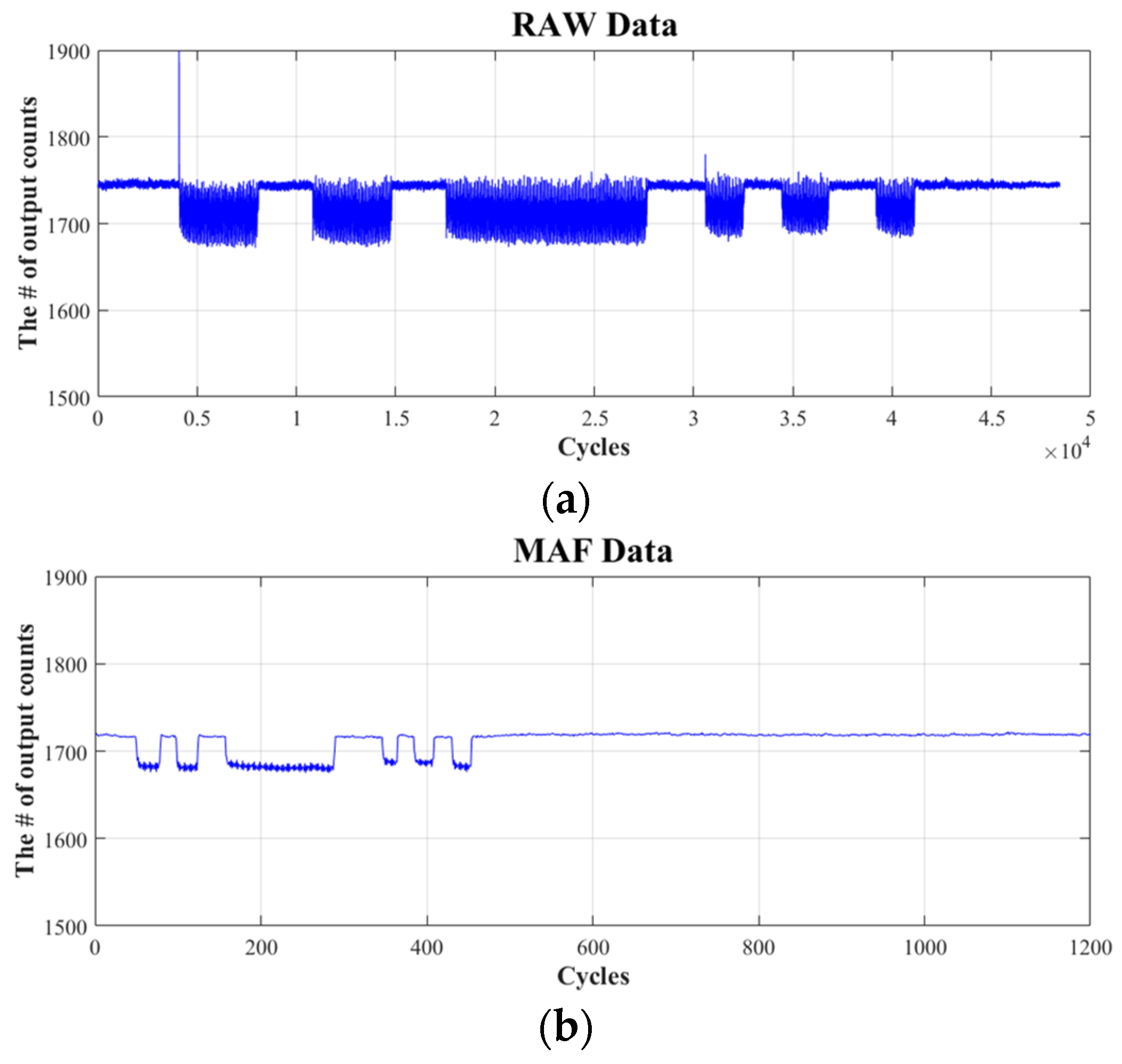
3.1. Moving Average Filter

The basic purpose of the MAF is to focus only on meaningful events by filtering out almost constant output fluctuations at the counter. Since the core idea of the MAF lies in generating the average counter output over a predefined period of time, changes that occur within a relatively short time in the counter output will be filtered and disappeared. These properties effectively suppress the impact of supply noise or minor human movement detected by the electrode. This noisy input is typically filtered through analog active LPFs with amplifiers that require a lot of power and area consumption. In addition, the output signal from the comparator used in the proposed system operates as a pulse, so an intermediate conversion process is required when using analog filters. The behavior of the MAF can be described by a simple equation as follows:
y [ n ] = n = 0 M 1 x [ n ] M
where n denotes each point, and M is the number of inputs used to calculate the average output (512 in the proposed design).
A detailed implementation of the MAF in the proposed system is shown in Figure 4a. The input and output signals of the MAF are 12 bit data of the counter output (D<11:0>) and the average output consisting of 12 bit data (Davg<11:0>) of the MAF unit, respectively. To generate the average number, a multi-bit full adder and a 21 bit accumulation register were used, which accumulated the counter output received 512 times for the 4096 / f C L K period. Here, 4096 / f C L K means the time required to count the number of comparator output pulse streams and generate a counter output signal once. After accumulating 512 counter outputs, only the first 12 MSB bits of the accumulation register are stored in the output register every 512 × 4096 / f C L K cycle. In the proposed system, the transfer characteristics of the MAF, an LPF, can be explained by a simple mathematical model. Figure 4b shows the frequency response of the MAF through MATLAB. Based on the simulation study, the 3 dB bandwidth was estimated to be 10 Hz, where the bandwidth of the digital filter is mainly determined by the number of bits of the counter output (12 in this design that comes from 212 = 4096) and the cumulative number of average outputs (nine in this design that comes from 2 9 = 512 ). The bandwidth of the MAF can be written as:
B W = f C L K / 2 m 2 n
where f C L K is the operating clock frequency (20 MHz in this design), m is the number of bits of the counter outputs ( m = 12 in this design), and n is the number of bits of average outputs ( n = 9 in this design). Based on Equation (4), the bandwidth was estimated to be approximately 9.5 Hz; accordingly, the power of the signal component outside this point decreases.

3.2. ΔC Detection Algorithm

The output filtered from the MAF unit is transmitted to the ΔC detection unit every 512 × ( 4096   / f C L K ) cycle. A circuit diagram and algorithm flowchart of the proposed Δ C detector are shown in Figure 5a,b, respectively. The Δ C detection unit basically calculates the difference between the present and previous MAF outputs (Davg<11:0>), representing the C s e n s i n g capacitance. That is, the Δ C detector can detect the C s e n s i n g capacitance variation (“ Δ C”) every 512 × ( 4096 / f C L K ) cycle. Then, the ΔC is compared to a predetermined amount of “Δ” in the next state, “k-bit magnitude comparators”, and through this, it is confirmed whether a current change in capacitance occurs (1) by contacting the human body or some object for a long time (touch/release decision) or (2) by the movement of some object (including humans) near the electrode (move decision).
Now, the ΔC detection algorithm based on the flowchart in Figure 5b is as follows. As explained, the output of the subtractor literally represents “ΔC” or capacitance fluctuation, which is obtained by calculating the difference between the MAF output of the current cycle and the previous cycle. The following comparator and logic part continue to monitor changes in C s e n s i n g , and if some changes occur in the current C s e n s i n g compared to the previous C s e n s i n g , the system determines the action taken against changes in the electrode capacitance. To explain a more detailed operation, first consider a case where the ΔC has a positive value, that is, Δ C > 0 . To be more specific, two possible scenarios are assumed and simulated. First, the electrode is touched by some objects, and this incurs the changes in the sensing capacitance abruptly at the beginning, but no further changes in capacitance happen. This case is called object detection. Second, the electrode now is being touched by a human, which also brings a sudden change in sensing capacitance. Moreover, the capacitance would be changed even after the initial contact to mimic the natural capacitance variation with a human body. This will be referred to as the human interaction case. Here, the capacitance variation after the initial contact is sufficiently larger than the variation due to the environmental noise, but its magnitude is managed to be smaller than the initial contact or release action.
In the first case, if the electrode capacitance is changed due to the fact of object contact, the magnitude comparators for touch/release decision and move decision compare the received ΔC with predetermined threshold levels, Δ C t o u c h and Δ C m o v e , respectively. If the ΔC of the subtractor exceeds each threshold level, the output of each comparator is in a high-level state. The given situation was simulated, and the resulting waveform is shown in the left half of Figure 5c. As shown in the figure, the touch and move signals were activated immediately after the capacitance value detected at the A1 position increased significantly. When the move pulse transitions to a high level, this signal generates a time reset pulse to reset the corresponding internal timer (TCON). The touch signal remains high until the timer output is activated. Unless there is an additional movement detection, the touch detection signal is zeroed by the timeout signal at the A2 position. Compared to the previous object detection scenario, the human interaction case shows a continuous movement detection pulse due to the situation described before. This additional move signal is transmitted to the TCON and keeps the touch sensing signal high. This situation is shown in the right half of Figure 5c. Therefore, the proposed Δ C detection algorithm can distinguish between object interaction and human interaction using move signals.
The remaining operation is when the ΔC becomes negative. This situation is normally related to the touch release action, and the capacitance detected is greatly reduced because the electrode does not contact the object or the human body. The operation of the proposed touch sensing system is described on the left side of the flowchart in Figure 5b. If ΔC is less than 0 ( Δ C < 0 ), the magnitude comparator for the touch/release decision unit compares the current |ΔC| with a Δ C r e l e a s e , a predetermined threshold for release action. Then, when | Δ C | > Δ C r e l e a s e , the system considers this situation as a real touch release operation and generates a release signal (not shown in the waveform). Accordingly, the touch signal returns to zero.

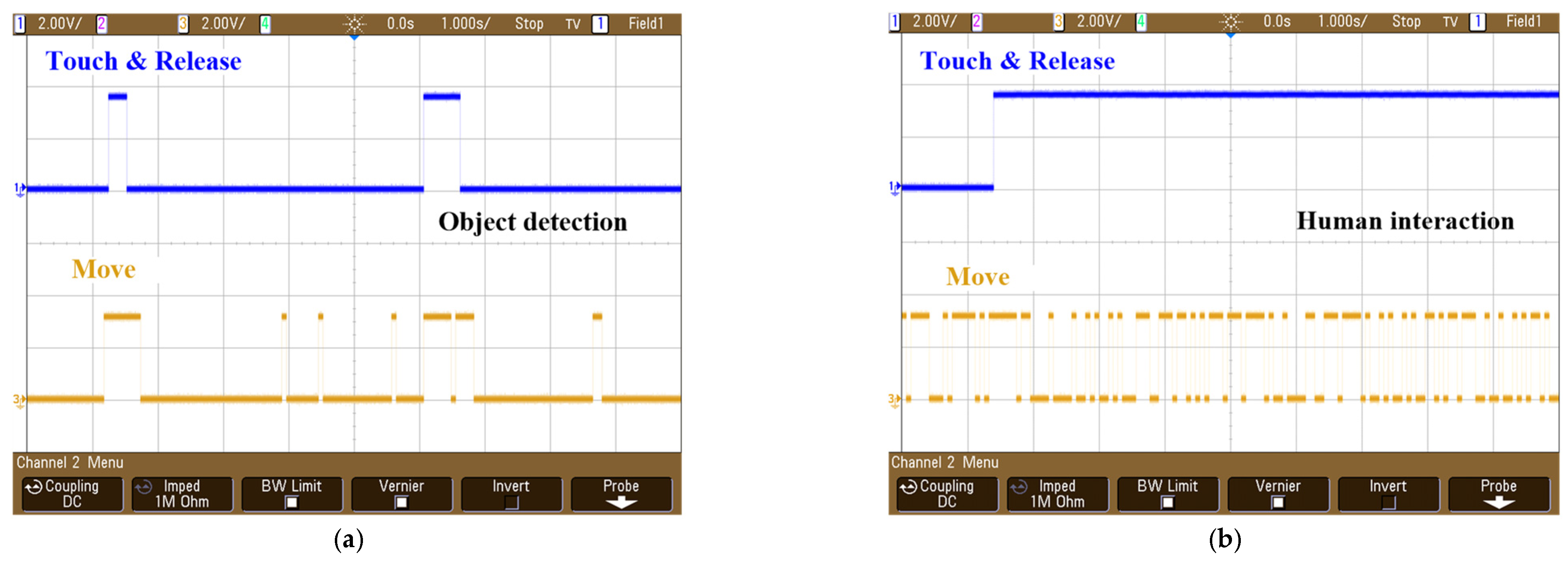
4. Measurement Results

A prototype of the proposed capacitance readout circuit was implemented using commercial 65 nm CMOS technology. Figure 6a shows the chip microphotograph, and Figure 6b represents the layout view of the core part (excluding the global power line connection part and the power capacitors). The total area consumed by the core part was 0.0067 mm2, wherein the sensing part and the filtering and detection parts accounted for 41% and 59% of the total area, respectively.
The chip measurement setup is shown in Figure 7. The system is powered by the CR2032 battery to model the HBC system and uses an external electrode from the Microchip MTCH101 evaluation kit. The performance of the proposed system was verified using a microcontroller and an oscilloscope (Digilent Analog Discovery 2). The microcontroller is responsible for the transaction of necessary input (e.g., the digital code corresponding to the capacitance threshold level) and output information through SPI communication and monitors the resulting output signal of the test chip using an oscilloscope. In addition, several LEDs are used to clearly visualize the current sensing output such as touch or movement detection results.
In order to verify the basic functionality of the proposed sensing system, the electrode was first touched several times with a finger. Figure 8a shows the raw counter output data, nominally staying at approximately 1750 and falling below 1700 when touched with a finger. These results are consistent with the previous description in Figure 3 in which the larger the electrode capacitance, the later the V X ( n ) node reached the critical level and reduced the number of output pulses from the comparator. When raw data were filtered using an MAF, the corresponding output waveform is shown in Figure 8b. As shown in the figure, the filter output of the MAF unit clearly shows the transition between the touched and untouched case without noise. The x-axes of the two graphs are not the same, because the MAF data show the filtered output signal in a compressed form.
Next, MAF output data were monitored in various situations. Figure 9a,b,c show the measured MAF output data for various situations. (1) Instead of direct contact with the electrode, the hand approaches the electrode and checks the system’s response as a proximity sensor. This will be referred to as motion detection hereafter. Next, the output of the system was monitored with (2) an object placed on the electrode, (3) an object placed on the electrode and, at the same time, the electrode was touched several times by hand. In the case of movement detection (Figure 9a), the MAF output data fluctuated between 200 and 600 cycles slightly. For object detection (Figure 9b), a smartphone was placed on the electrode at approximately 300 cycles. As a result, the electrode capacitance increased (i.e., the MAF output data decreased), and the MAF data became a new steady state. However, if the electrode was touched with a finger while the smartphone was still placed, the proposed capacitive sensing system could detect a human touch even after the MAF output data reached a new steady state by the smartphone. As can be seen in Figure 9c, the MAF data show a reduced steady state after detecting an object at 200 cycles and continued to detect human interactions seen as an additional sharp drop in MAF data even in a new steady state. Note that the irregular pattern of a sharp drop is a natural behavior that can be expected from human interaction because human contact continuously changes C s e n s i n g in an unexpected way, resulting in changes in counter output.
While the output from the MAF device intuitively shows the system’s different responses to object detection and human interaction, the output data still represent the average number of counter outputs as multi-bit binary numbers that are difficult to use in other parts of the systems. However, similar responses can be monitored in the two output signals from the magnitude comparator in Figure 5a.
The two output signals are a touch/release detection signal and a movement detection signal, respectively. The two measured signals are shown in Figure 10a,b. Figure 10a shows the change in the two signals when an object was placed on an electrode, and in the case of a movement signal, only a few pulses appeared at the beginning. As described in the flowchart in Figure 5b, since there is no further variation in the movement signal, the touch/release signal became zero over time. On the other hand, when there was human interaction, the movement signal continuously showed irregular fluctuations, so the touch/release signal remained high. Representing the detected situation with two different signals allows the system to interact with other digital parts without additional decoding steps, which is a great advantage of the proposed system.
Table 1 summarizes the performance of the proposed capacitive sensing system and compares it with other prototypes [15,16,17] and commercial products (Azoteq IQS211A/B and Microchip MTCH101). The proposed system adopts MAF, a digital low-pass filter, to enhance noise immunity without including ADCs that consume a lot of area and power. In addition, the Δ C detection algorithm based on simple digital logic allows the system to distinguish human interactions and interactions with objects with only a few resources.
The proposed system consumed 7.5 uW of power and occupied an area of 0.0067 mm2. The relatively low area and power consumption of the proposed system compared to competitors in similar application ranges demonstrate the efficient use of resources. Even though the commercial product (Azoteq IQS211A/B) appears to consume slightly less power than the proposed system, the system may misdetect the situation due to the lack of built-in noise filtering.
Lastly, the response time of the proposed system was measured as 105 ms, which can be expected in the bandwidth calculation based on Equation (4). Note that 105 ms of time is short enough to detect human interactions. However, the proposed system can adaptively change the response time by changing the cumulative number of steps in the MAF and Δ C detection parts at the expense of noise immunity and accuracy.

5. Conclusions

This paper proposed an area-efficient and low-power capacitive readout circuit for human interaction detection. The proposed system consisted of a “sensing part” and a subsequent “filtering and detection part”. The sensing part served to measure the capacitance of the touchpad (electrode) through charge sharing between the sensing capacitor and the sampling capacitor. The resulting comparator output behaved like a periodic pulse stream, and the number of pulses generated by the comparator was monitored at the next stage of the filtering and detection part for a certain period of time, reflecting the magnitude of the detected capacitance.
Regarding the filtering and detection part, a digital logic-based MAF was adopted in the proposed design to eliminate the inherent noise-induced fluctuations in detected capacitance values, i.e., variations in the number of comparator output pulses. In addition, the type and intensity of touch at a specific moment were analyzed based on the proposed ΔC detection algorithm.
The prototype chip of the capacitive sensing system was fabricated in 65 nm process technology, while the system consumed 7.5 uW of power and occupied an active area of 0.0067 mm2; the response time of the system was measured to be 105 ms. The power consumption of the proposed system could be potentially lower further by adopting a sleep mode operation. During sleep mode, the operation of the proposed capacitive sensing system would be slowed to optimize total power consumption. However, when a touch event is detected, the system immediately shuts down the power-saving mode and operates under normal conditions. In addition, the scope of application of the proposed system will be expanded if the system can accurately measure the magnitude of capacitance at high resolution.
In conclusion, the concise structure of the proposed capacitive sensing system and its corresponding low-power and noise-robust characteristics will pave the way for an energy-efficient human body communication system.

Author Contributions

Conceptualization, methodology, and validation, S.-W.C. and K.S.; investigation, resources, and data curation, S.L. and K.-H.B.; writing—original draft preparation, S.-W.C.; writing—review and editing, K.-H.B. and Y.S.; supervision and project administration, Y.S. All authors have read and agreed to the published version of the manuscript.

Funding

This work was supported in part by Chung-Ang University Research Grants in 2020, in part by a Korea Institute for Advancement of Technology (KIAT) grant funded by the Korea Government (MOTIE) (P0017011, HRD Program for Industrial Innovation), and in part by a National Research Foundation of Korea (NRF) Grant funded by the Korea Government (MSIT) under Grant 2020R1A2C1012714.

Conflicts of Interest

The authors declare no conflict of interest.

References

  1. Zhao, J.F.; Chen, X.M.; Liang, B.D.; Chen, Q.X. A review on human body communication: Signal propagation model, communication performance, and experimental issues. Wirel. Commun. Mob. Comput. 2017, 2017, 15. [Google Scholar] [CrossRef] [Green Version]
  2. Das, D.; Maity, S.; Chatterjee, B.; Sen, S. Enabling covert body area network using electro-quasistatic human body communication. Sci. Rep. 2019, 9, 1–14. [Google Scholar] [CrossRef]
  3. Kang, T.; Oh, K.-I.; Hwang, J.-H.; Kim, S.; Park, H.; Lee, J. Measurement and analysis of electric signal transmission using human body as medium for WBAN applications. IEEE Trans. Instrum. Meas. 2018, 67, 527–537. [Google Scholar] [CrossRef]
  4. Kang, T.; Hwang, J.-H.; Kim, H.; Kim, S.-E.; Oh, K.-I.; Lee, J.-J.; Park, H.-I.; Kim, S.-E.; Oh, W.; Lee, W. Measurement and Evaluation of Electric Signal Transmission through Human Body by Channel Modeling, System Design, and Implementation. IEEE Trans. Instrum. Meas. 2021, 70, 1–14. [Google Scholar] [CrossRef]
  5. Kang, T.; Oh, K.-I.; Lee, J.-J.; Park, B.-S.; Oh, W.; Kim, S.-E. Measurement and Analysis of Human Body Channel Response for Biometric Recognition. IEEE Trans. Instrum. Meas. 2021, 70, 1–12. [Google Scholar] [CrossRef]
  6. Tan, Z.; Jiang, H.; Zhang, H.; Tang, X.; Xin, H.; Nihtianov, S. Power-Efficiency Evolution of Capacitive Sensor Interfaces. IEEE Sens. J. 2020, 21, 12457–12468. [Google Scholar] [CrossRef]
  7. Tan, Z.; Shalmany, S.H.; Meijer, G.C.; Pertijs, M.A. An energy-efficient 15-bit capacitive-sensor interface based on period modulation. IEEE J. Solid-State Circuits 2012, 47, 1703–1711. [Google Scholar] [CrossRef]
  8. He, Y.; Chang, Z.-Y.; Pakula, L.; Shalmany, S.H.; Pertijs, M. 27.7 A 0.05 mm 2 1V capacitance-to-digital converter based on period modulation. In Proceedings of the 2015 IEEE International Solid-State Circuits Conference-(ISSCC) Digest of Technical Papers, San Francisco, CA, USA, 22–26 February 2015; pp. 1–3. [Google Scholar]
  9. Jung, W.; Jeong, S.; Oh, S.; Sylvester, D.; Blaauw, D. 27.6 A 0.7 pF-to-10nF fully digital capacitance-to-digital converter using iterative delay-chain discharge. In Proceedings of the 2015 IEEE International Solid-State Circuits Conference-(ISSCC) Digest of Technical Papers, San Francisco, CA, USA, 22–26 February 2015; pp. 1–3. [Google Scholar]
  10. Cong, P.; Chaimanonart, N.; Ko, W.H.; Young, D.J. A wireless and batteryless 10-bit implantable blood pressure sensing microsystem with adaptive RF powering for real-time laboratory mice monitoring. IEEE J. Solid-State Circuits 2009, 44, 3631–3644. [Google Scholar] [CrossRef]
  11. Jiang, H.; Wang, Z.; Zhang, C.; Jiang, H.; Wang, Z. A combined low power SAR capacitance-to-digital analog-to-digital converter for multisensory system. Analog Integr. Circuits Signal Processing 2013, 75, 311–322. [Google Scholar] [CrossRef]
  12. Ha, H.; Sylvester, D.; Blaauw, D.; Sim, J.-Y. 12.6 A 160nW 63.9 fJ/conversion-step capacitance-to-digital converter for ultra-low-power wireless sensor nodes. In Proceedings of the 2014 IEEE International Solid-State Circuits Conference Digest of Technical Papers (ISSCC), San Francisco, CA, USA, 9–13 February 2014; pp. 220–221. [Google Scholar]
  13. Yang, R.; Pertijs, M.A.; Nihtianov, S. A precision capacitance-to-digital converter with 16.7-bit ENOB and 7.5-ppm/°C thermal drift. IEEE J. Solid-State Circuits 2017, 52, 3018–3031. [Google Scholar] [CrossRef]
  14. Narasimman, N.; Nag, D.; Chuan, K.C.T.; Kim, T.T. A 1.2 V, 0.84 pJ/conv.-Step ultra-low power capacitance to digital converter for microphone based auscultation. In Proceedings of the 2017 IEEE Custom Integrated Circuits Conference (CICC), Austin, TX, USA, 30 April–3 May 2017; pp. 1–4. [Google Scholar]
  15. Narasimman, N.; Nag, D.; Chai, K.T.; Kim, T.T.-H. A Capacitance to Digital Converter using Continuous Time ΔΣ Modulator for Microphone-based Auscultation. IEEE Sens. J. 2021, 21, 13373–13383. [Google Scholar] [CrossRef]
  16. Liu, B.; Hoseini, Z.; Lee, K.-S.; Lee, Y.-M. On-chip touch sensor readout circuit using passive sigma-delta modulator capacitance-to-digital converter. IEEE Sens. J. 2015, 15, 3893–3902. [Google Scholar] [CrossRef]
  17. Asgari, M.; Lee, K.-S.; Lee, Y.-M. Touch sensor readout circuit with comparator threshold self-adjustment. IEICE Electron. Express 2018, 15, 20171065. [Google Scholar] [CrossRef] [Green Version]
Figure 1. Capacitive coupling-based human body communication (HBC) systems.
Electronics 11 00577 g001
Figure 2. (a) Overall architecture of the proposed capacitance readout circuit; (b) timing diagram.
Electronics 11 00577 g002
Figure 3. Sensing mechanism of the capacitance readout circuit for: (a) an untouched case; (b) a touched case.
Electronics 11 00577 g003
Figure 4. (a) Circuit diagram of the moving average filter (MAF); (b) its frequency response.
Electronics 11 00577 g004
Figure 5. (a) The circuit diagram; (b) the flowchart of the ΔC detection algorithm; (c) ΔC detection algorithm simulation results.
Electronics 11 00577 g005
Figure 6. (a) Chip microphotograph; (b) core layout.
Electronics 11 00577 g006
Figure 7. The chip measurement setup.
Electronics 11 00577 g007
Figure 8. (a) Raw data; (b) MAF data when a finger touches the electrode with the same pattern.
Electronics 11 00577 g008
Figure 9. The MAF data of (a) movement interaction; (b) object detection; (c) human interaction while an object is on the electrode.
Electronics 11 00577 g009aElectronics 11 00577 g009b
Figure 10. Capacitance readout circuit output waveforms when (a) an object is on the electrode; (b) a finger touches the electrode.
Electronics 11 00577 g010
Table 1. Performance comparison table.
This Work[16][17][15]Azoteq
IQS211A/B 3
Microchip
MTCH101 3
Process (nm)65350350180--
Supply Voltage (V)1.23.33.31.23.33.3
Area (mm2)0.00670.10.00270.42--
ApplicationsTouch and
Proximity
Touch PanelTouch PanelPressure
Sensor
Touch and
Proximity
Touch and
Proximity
ADC-FreeOOOXXX
Noise ImmunityOOXOXX
Object DetectionOXXXOX
Power (uW)7.5655250.4254.16.6660178.2
LPF BW (Hz)610.49.51000 1-4000----
Response Time (ms)1.610520 220 20.125916080640
1 Estimated from the paper; 2 scanning rate; 3 commercial products.
Publisher’s Note: MDPI stays neutral with regard to jurisdictional claims in published maps and institutional affiliations.

