Article

Development of Voltage Control Algorithm for Improving System Stability in Korean Distribution Grids

1
School of Electronical and Electrical Engineering, Daegu Catholic University, Daegu 38430, Republic of Korea
2
KEPCO Research Institute, Daejeon 34056, Republic of Korea
*
Author to whom correspondence should be addressed.
Electronics 2022, 11(22), 3661; https://doi.org/10.3390/electronics11223661
Submission received: 25 October 2022 / Revised: 3 November 2022 / Accepted: 7 November 2022 / Published: 9 November 2022
(This article belongs to the Special Issue Smart Energy Control & Conversion Systems)

Abstract

:
Problems with overvoltage and reverse energy flow arise as the percentage of distribution energy resources (DERs) in distribution system rises. This paper implements a MATLAB/Simulink linked model that communicates with the OpenDSS engine. The point of common coupling (PCC) voltage typically mitigates using the inverter outputs control. However, case overvoltage issues occur in distribution networks and the influence of the volt–var control effect is insufficient to reduce PCC voltage to a stable range. To improve the reactive control effect, this paper proposes active power control and voltage error compensation methods that maximize the reactive power control effect. The DER management system (DERMS) platform was constructed to analyze the effect of changing DER output values. The DERMS data are organized based on real distribution line (D/L) system data where overvoltage occurred in Korea and the control effect of the real system is analyzed. This control method analysis can be used to develop an inverter control scheme for the over voltage issues described in this paper.

1. Introduction

Energy strategies are currently promoted with the increase in the amount of natural gas and renewable energy sources, as well as with the increase in energy efficiency. Moreover, government initiatives have recently promoted innovative and sustainable energy sources. The domestic “renewable energy 3020 implementation plan” plans to increase the proportion of renewable energy production to about 20% by 2030. Since the proportion of renewable energy production is currently lower than the large countries, the government intends to achieve its goal by supplying clean energy, such as solar and wind power, to more than 95% of new facilities [1]. Additionally, distribution energy resources (DERs) connected to small distribution systems are becoming increasingly popular due to their rapid construction and low-cost benefits [2].
However, photovoltaic (PV) generation active power output depends on solar radiation and unexpected solar radiation power output causes unstable power outages. Furthermore, low-voltage and over-voltage problems may occur in a power distribution system [2]. Several techniques have been proposed to alleviate the voltage problem caused by the DER located in a power distribution system. A common technique for mitigation is to use an on-load tap changer and a step voltage regulator to resolve overvoltage issues. These voltage control assets are efficient in conventional general distribution networks. However, voltage has recently increased at the end of distribution networks due to PV generation and the voltage control effect cannot be expected on the line with changing characteristics. In the conventional distribution network voltage profile, the measured voltage is low since the voltage measurement point is far from the voltage source. Currently, the voltage rises at the end of the distribution line. Therefore, the DER connection leads to overvoltage problems, such as reverse power flow (RPF), in the distribution network. As a result, it is important to consider the voltage problem for bidirectional power flow and to improve the stability of the distribution network for situations with many variables [3].
A smart inverter is an inverter capable of autonomously controlling and supporting DER output. Smart inverters work to make the distribution network stable and their features include fixed-power factor control, voltage–var control, volt–watt control, frequency–watt control, voltage ride-through, frequency ride-through, and manual active and reactive power control. The autonomous operational functions required for system stabilization were derived in IEEE 1547-2018. The operation of test techniques and inspection criteria were presented to create a way to use a communication interface based on IEC 61850-7-520 with key input parameters of volt–var control (VVC) and volt–watt control (VWC) [4,5]. The VVC control method adjusts the point of common coupling (PCC) voltage of the PV inverter. According to the VVC curve set in advance, the inverter controls the reactive power to absorb or supply itself. Moreover, the VWC method uses the PCC of the PV inverter. It determines the active power output depending on the voltage of the inverter based on the VWC curve and whether the converged PCC voltage is in a stable range.
The inverter control method using VVC was studied in [6,7,8]. In the case of PCC voltage, VVC is effective for lowering the voltage. The VWC control effect was confirmed in [9,10]. The PCC voltage is in an unacceptable range. The reduction in PV system active power then mitigates the voltage rise. In particular, VVC and VWC have been shown to be reasonable approaches to mitigate the voltage rise in terms of effectiveness. In practice, however, reducing the active power output with VWC can lead to financial problems for PV system holders and the reactive power output curve may also be conservatively set to fail to track the maximum power output [11].
A previous study economically investigated how to configure a distributed energy resource management system (DERMS) with actual North American distribution feeder data while minimizing curtailment [12]. Moreover, these researchers made predictions through analyzed studies on curtailment uncertainties arising from renewable energy [13]. Most conventional studies focus on the economic perspective of reduction and research is mainly aimed at improving economic feasibility by minimizing curtailment [14,15,16].
In this paper, we implement DERMS while applying a control technique to improve distribution line stability from the system stability perspective. Recently, distributed energy resources installed in Korea have been connected on a large scale and have faced difficulty in maintaining system stability and electrical quality. Therefore, it is most efficient to spread hierarchically controllable smart inverters to solve the problem of high variability in distributed energy resources [3]. The DERMS control aims to maximize the stability of the DERs. Therefore, voltage error correction is implemented to maximize the reactive power output that outputs the control method. The voltage error compensation controller proposed in this paper calculates the moving-average voltage to generate a reactive power value. If overvoltage persists afterwards, VWC is implemented. During VWC, the DERMS calculates the optimal active power output for each DER through PCC voltage and power changes.
To evaluate the implementation of the proposed DERMS and the voltage stabilization effect using real system data, the OpenDSS [17] engine is used. OpenDSS is an electric power distribution system simulator based on an open-source software developed by the Power Research Institute (EPRI). OpenDSS is suitable for quasi-static time series analysis using real systems and precise system data design. The DERMS model was implemented in MATLAB/Simulink, and the input and output of the smart inverter model communicates with the OpenDSS engine component object model. As a result of implementing an algorithm that performs active power control and reactive power hybrid control, it was confirmed that the overvoltage phenomenon of power distribution lines was effectively alleviated and the stability of the system was improved [4]. Finally, the DERMS can curtail the active power of a smart inverter. The upper layer determines and commands the output for the optimal active power output of a smart inverter in accordance with South Korea’s Distribution Network Voltage Management Regulations [18].
The remainder of this paper is organized as follows. Section 2 shows the control function of the smart inverter. Conventional voltage control methods for inverters are described in Section 3, while Section 4 proposes a method to maximize reactive power control performance through voltage error compensation. Section 5 describes the concept of DERMS and how to generate active power output limits in the modeling of voltage control systems. Section 6 analyzes the performance of the proposed algorithm and the DERMS control algorithm, and a summary of this paper and its contributions is provided in Section 7.

2. Voltage Control Method of a Smart Inverter

Depending on the PCC voltage of the smart inverter, the volt–var function regulates the supply and absorbs the reactive power. When overvoltage occurs and the voltage is lowered, the reactive power control monitors the PCC voltage and gradually increases the induced reactive power to raise the voltage. If the PCC voltage is an overvoltage, the capacitive reactive power is released, reducing the voltage [19,20].
The VWC controls the active power according to voltage fluctuations. This technique uses the measured PCC voltage. If the voltage exceeds the stable voltage range, the VWC adjusts the active power output to reduce the voltage. The VWC function is used simultaneously with the VVC function or when an overvoltage occurs after VVC.
The voltage stabilization process of the distribution network is mainly achieved through the control of the reactive power. Where the VVC is used, it is possible to autonomously adjust the reactive power output based on the PCC voltage of the DER. The reactive power of the inverter is automatically determined according to the definition of Q–V droop control. In addition, the inverter PCC voltage measurement and reactive power control are performed. The voltage of the DER is stabilized by the generated reaction power and this procedure is continuously repeated in the smart inverter.
This method converges to a stable operating point, which is valuable for stable operation. Reactive power control through the VVC curve is characterized by tracking the stable reactive power output and the final convergent voltage value is determined by the characteristics of the system connection point of the smart inverter, i.e., the Thevenin equivalent impedance, active power values, and reactive power values.

3. Conventional Voltage Control Method

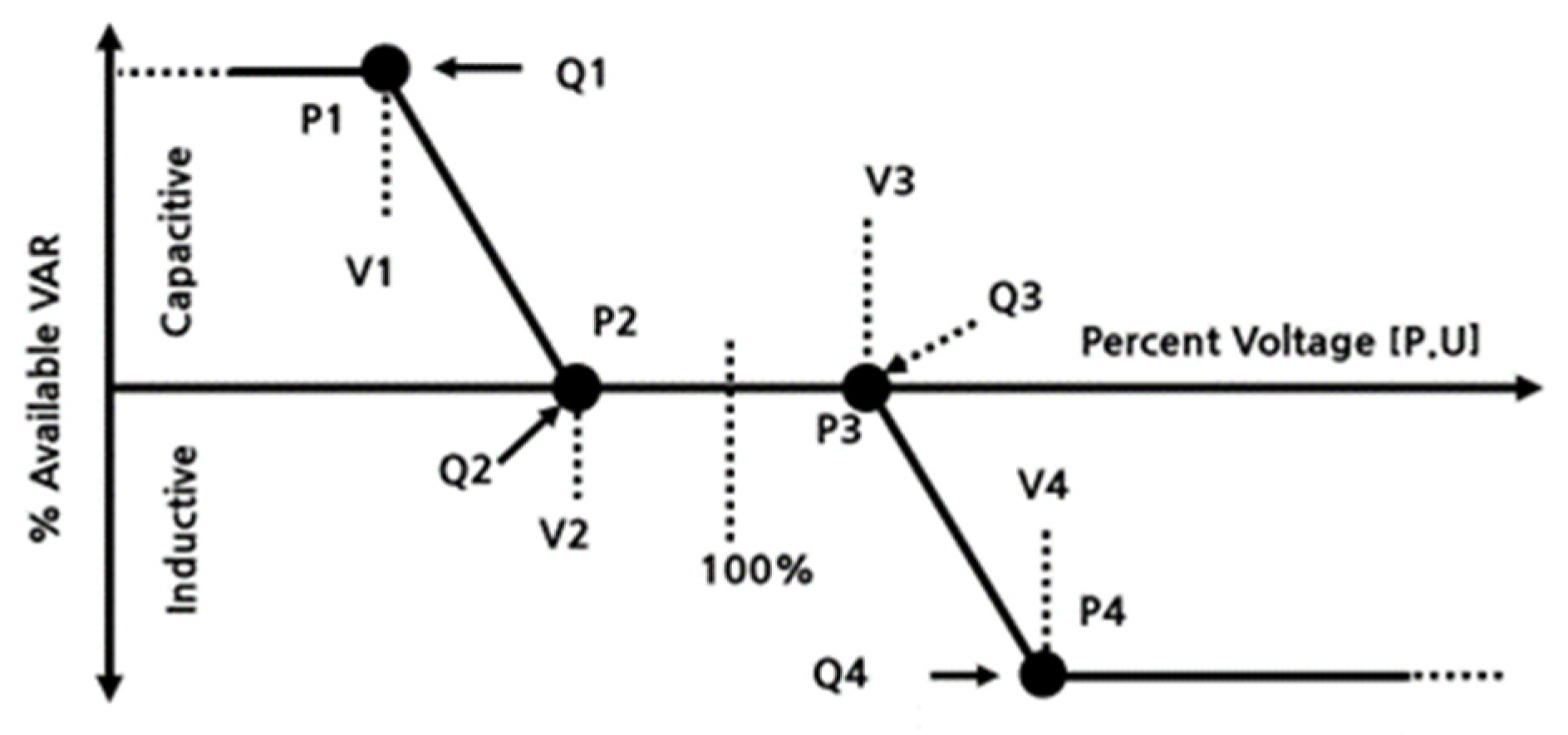
3.1. Volt–Var Control (VVC)

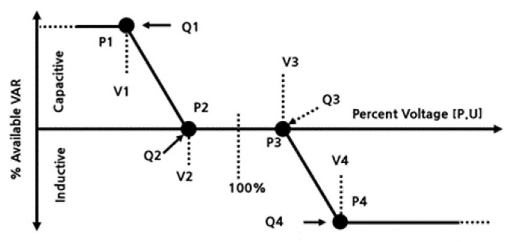
3.1.1. Definition of Volt–Var Control

VVC is a function of autonomously generating reactive power control for absorption or supply based on PCC voltage. If the PCC voltage is in the high voltage range, the inverter generates inductive reactive power. If the PCC voltage is in the low voltage range, the inverter generates capacitive active power. A typical volt–var curve is illustrated in Figure 1.
Furthermore, reactive power is generated based on the PCC voltage for each unit period while reactive power output is determined based on a preset VVC curve. In Figure 1, V1 is the boundary of the minimum PCC voltage (P1), V2 is the start of the low voltage set point (P2), V3 is the start of the high voltage set point (P3), and V4 is the boundary of the maximum PCC voltage (P4). The invalid power output setting should also consider inverter specifications; Q1 is the maximum capacitive power generation of the inverter and Q4 is the maximum induced power generation. The reactive power output is the dead zone where the outputs of Q2 and Q3 are zero in the voltage range from V2 to V3.

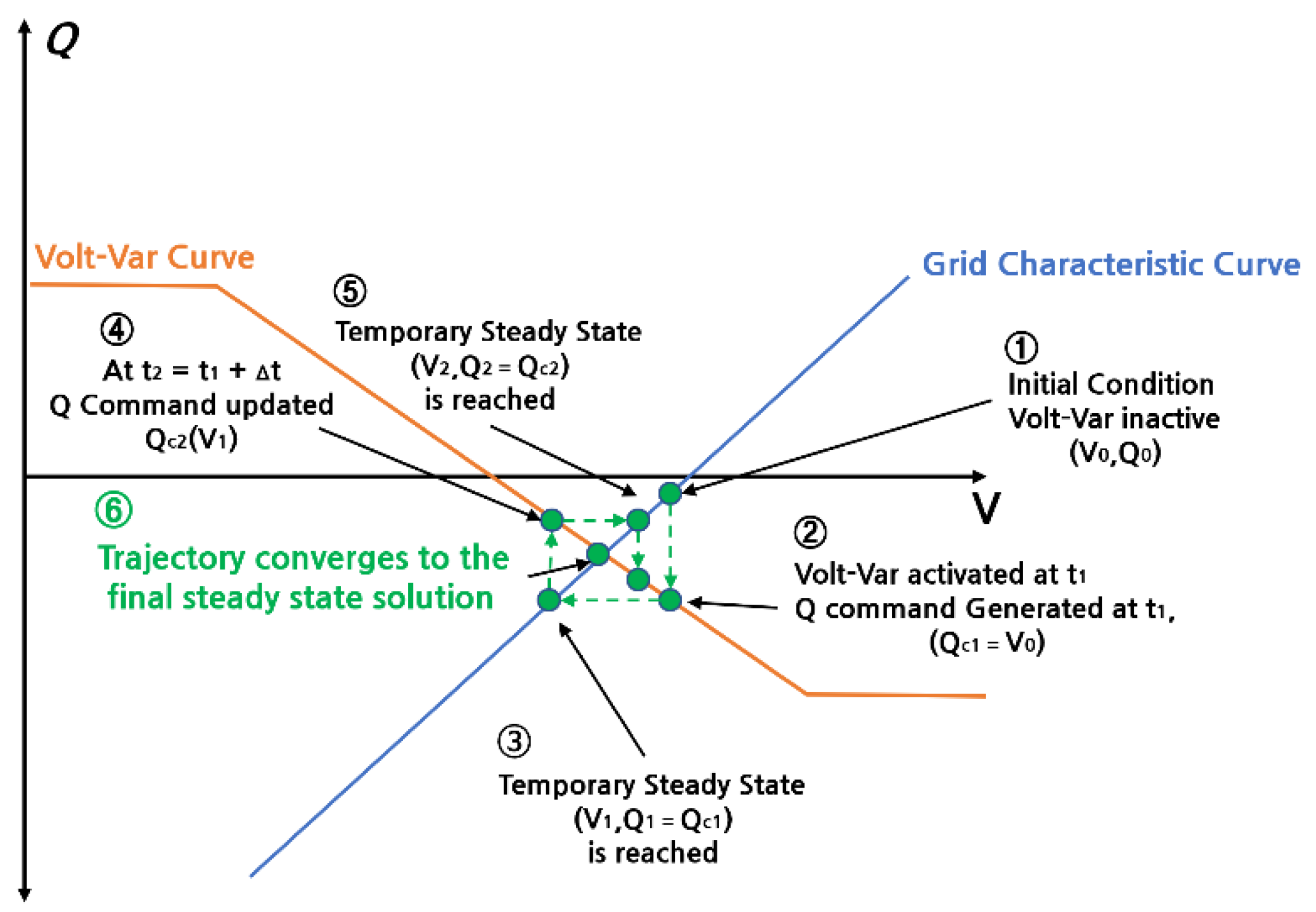
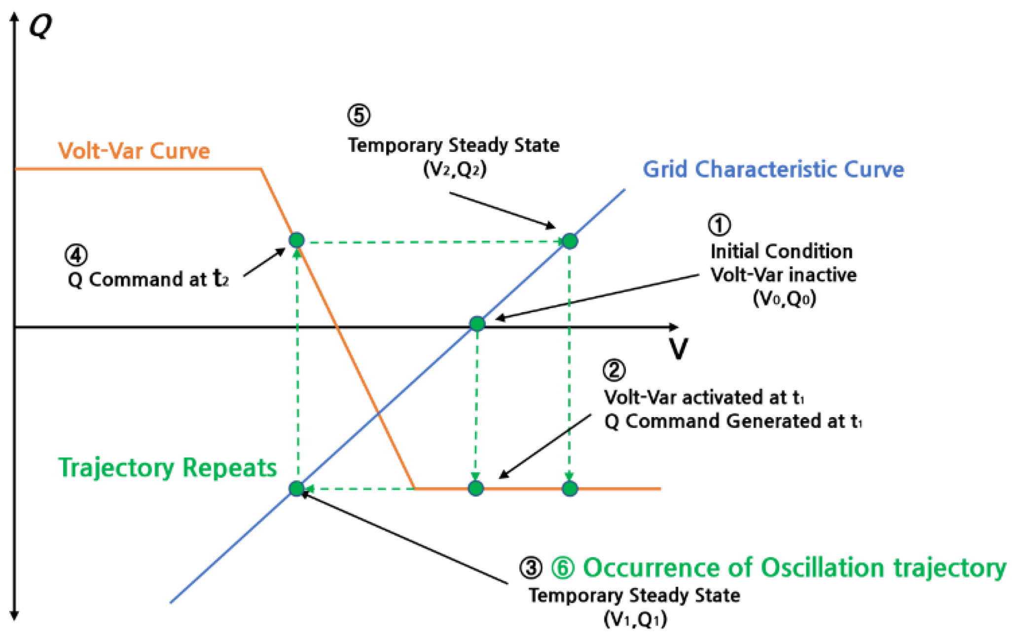
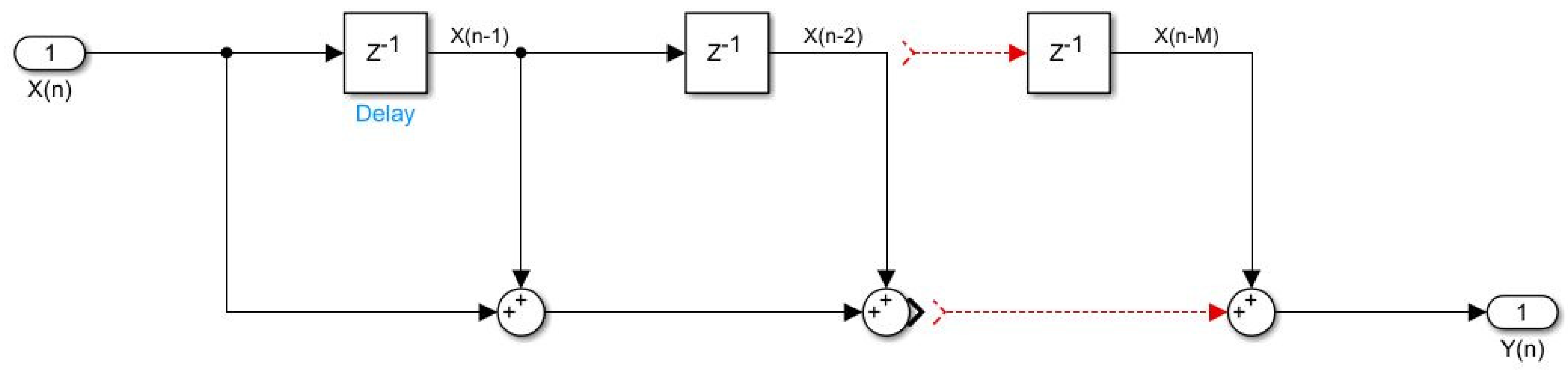
3.1.2. Stability Converging with VVC

Figure 2 illustrates the progress of stable operation point tracking. The grid characteristic curve (blue line in the figure) is the influence of inverter control at the PCC. Initial PCC voltages (V0, Q0) are determined by the Qc1 (V0) value of t1, which represents the reactive power output of the VVC for the voltage value of the system characteristic curve. In the next cycle, T2 = t1 + ΔT, the volt–var reaction power output value according to the grid characteristic curve is represented as Qc2 (V1), and the volt–var command value according to the grid characteristic curve is continuously generated with every cycle of ΔT. The VVC function continues to run until the volt–var characteristic curve converges [11,18,19,20].
According to the relationship between the slope of the VVC curve and the voltage characteristic curve, the requirements for convergence to a stable operating point are as follows:
S l o p e V o l t V a r < S l o p e G r i d e C h a r a c t e r i s t i c C u r v e .
However, if the slope of the VVC curve is adjusted steeply, voltage oscillation may occur in accordance with the conditions in Equation (2) and as illustrated in Figure 3.
S l o p e V o l t V a r > S l o p e G r i d e C h a r a c t e r i s t i c C u r v e
Figure 3 shows the case of unstable VVC operation. Due to the slope relationship between the volt–var curve and the grid characteristic curve, the reactive power output does not converge. It is important to select a volt–var curve gradient in which the voltage of the connection point converges for distributed power generation in order that a stable condition is achieved.

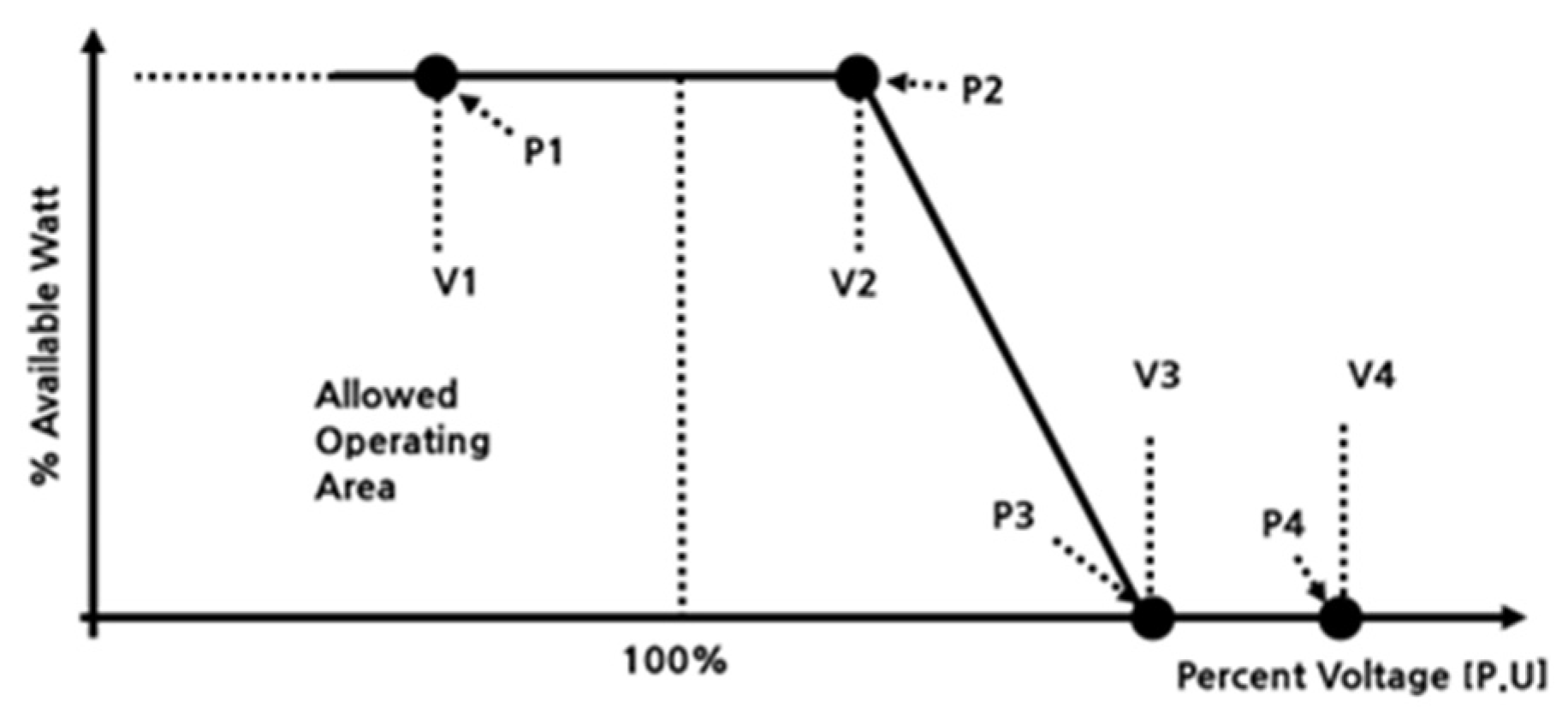
3.2. Volt–Watt Control (VWC)

VWC reduces active power autonomously based on PCC voltage. If the PCC voltage is in the high voltage range, the inverter reduces the active power output. PCC voltage and VWC curves are shown in Figure 4.
The active power output is generated based on a preset VWC curve. In Figure 4, V2 is the start of the high voltage set point (P2) and V3 is the boundary of the maximum PCC voltage (P3). Active power output is not reduced when the PCC voltage is in the stable range (P1). However, the active power output is completely cut off if there is a point above the maximum PCC voltage (P4). VWC is applied by limiting the maximum output in smart inverters and can directly and successfully reduce the PCC voltage [17,18].

4. Improved Voltage Control Methods

4.1. Voltage Error Compensation (VEC)

4.1.1. Definition of VEC

In general, a method using VVC has limitations in invalid output and causes a problem of insufficient control. VVC curve generation value is related to the characteristics of the distribution network. Therefore, Section 3 demonstrated that there are limitations to obtaining high voltage control performance. This study proposes a VEC method using the moving-average PCC voltage and the voltage–var reference voltage of an inverter.
The moving-average voltage is used to connect the average values of functions before and after each term in the time series and to calculate the average voltage of the PCC. Figure 5 illustrates the process of calculating the moving average. The operator can select a unit time for the moving-average voltage, such as 30 s, 1 min, or 5 min. The VEC controller collects moving-average voltage values and collects volt–var curve control reference voltage values to calculate voltage errors. A reactive power command value is generated for voltage error correction using a voltage error. The transmitted command value is limited to the generated reactive power command value in order not to exceed the maximum value of the reactive power output of the smart inverter.

4.1.2. VEC Curve Parameter Settings

The VEC model determines the reactive power output of the inverter based on the voltage error. The moving-average voltage of the PCC voltage is calculated to generate a voltage error between the moving-average voltage value and the VVC voltage reference point. The VVC voltage reference point indicates a point at which the overvoltage range starts. The voltage error is transmitted to the VEC curve and the reactive power output is determined.
Figure 6 shows the VEC curve, which is the difference between using a delta voltage and a VVC. A delta voltage is continuously generated by receiving PCC voltage and VVC curve information to the control block. The delta PCC voltage passing through the calculation block is transmitted to the VEC curve and the reactive power generated by the VEC curve is defined as follows:
Q V E C = Q 1 , Δ V P C C V 1 Q 1 Q 2 V 1 V 2 V P C C V 2 + Q 1 , V 1 Δ V P C C V 2 0 , V 2 Δ V P C C V 3 Q 3 Q 4 V 3 V 4 V P C C V 3 + Q 3 , V 3 Δ V P C C V 4 Q 4 , V 4 Δ V P C C .
In Equation (3), V 1 is the boundary of the minimum delta PCC voltage (P1), V 2 is the start of the low voltage set point (P2), V 3 is the start of the high voltage set point (P3), and V 4 is the boundary of the maximum PCC voltage (P4). In addition, the reactive power output setting is based on the inverter specification, where Q 1 is the maximum capacitive power generation and Q4 is the maximum induced power generation. The reactive power output is zero in the voltage range of V 2 to V 3 , and the dead zones are Q 2 and Q 3 . In contrast to VVCs, a dead zone setting is not mandatory for VECs. The process of moving-average operations generated based on unit time is not very volatile.
Table 1 shows the detailed VEC curve parameters applied in this paper. The VEC control curve sets the voltage range to effectively control overvoltage. Q m a x and Q m i n in Table 1 refer to the maximum supply and maximum absorption capacity of the inverter, respectively. In addition, the dead zone was set at ±0.01 p.u. in order that the reactive power output value could quickly converge. Ultimately, these parameter settings have the advantage of minimizing power fluctuations in low and overvoltage situations. In addition, it is possible to stably increase the output within the reactive power output range of the inverter.

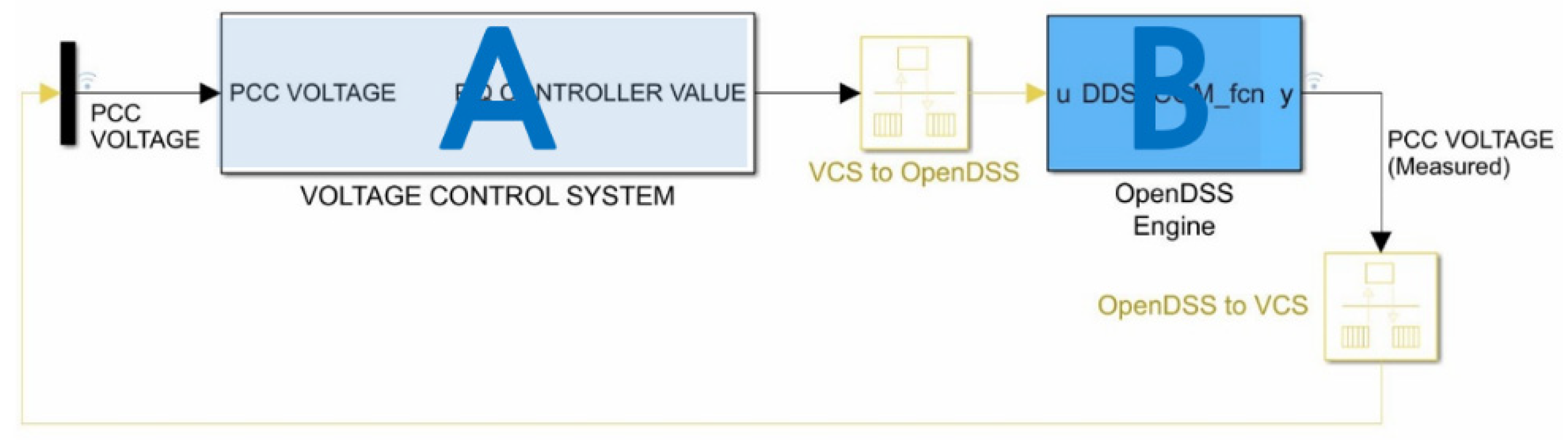
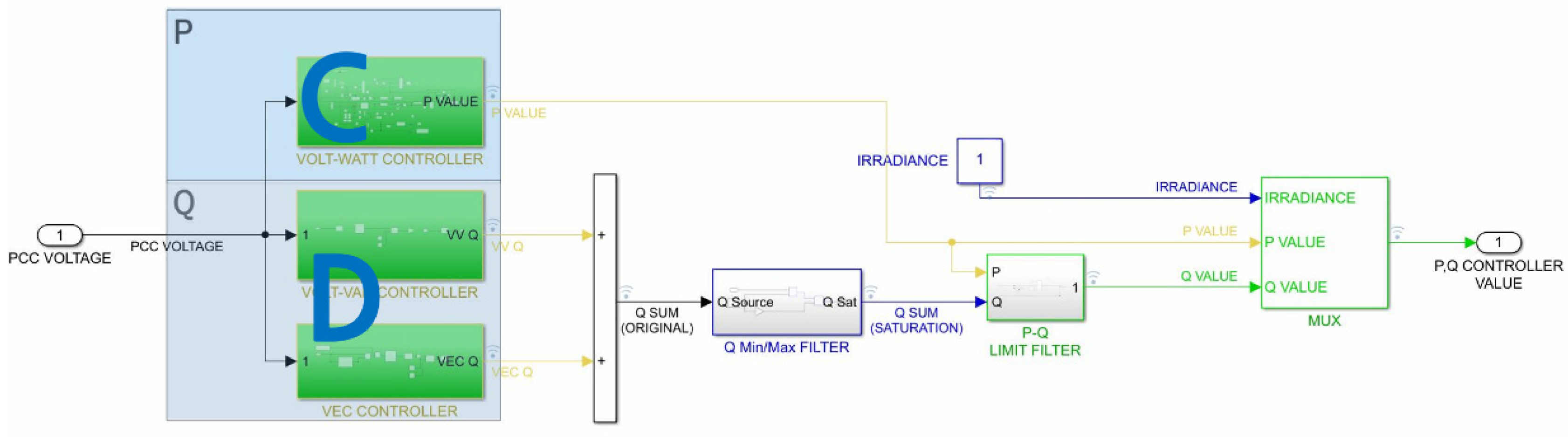
4.2. Voltage Control System (VCS) Model
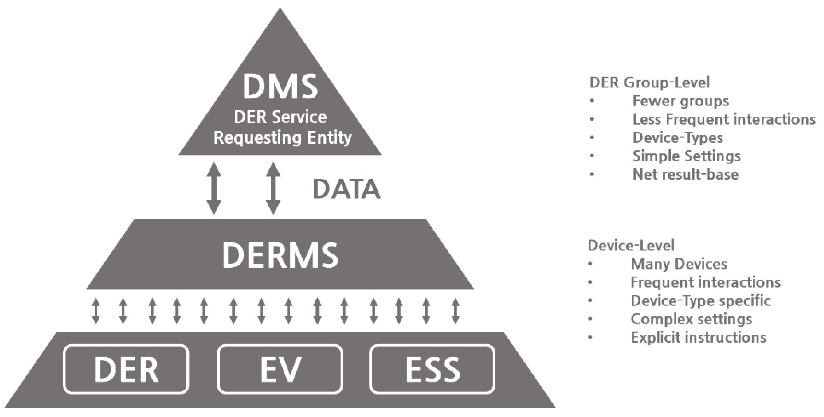
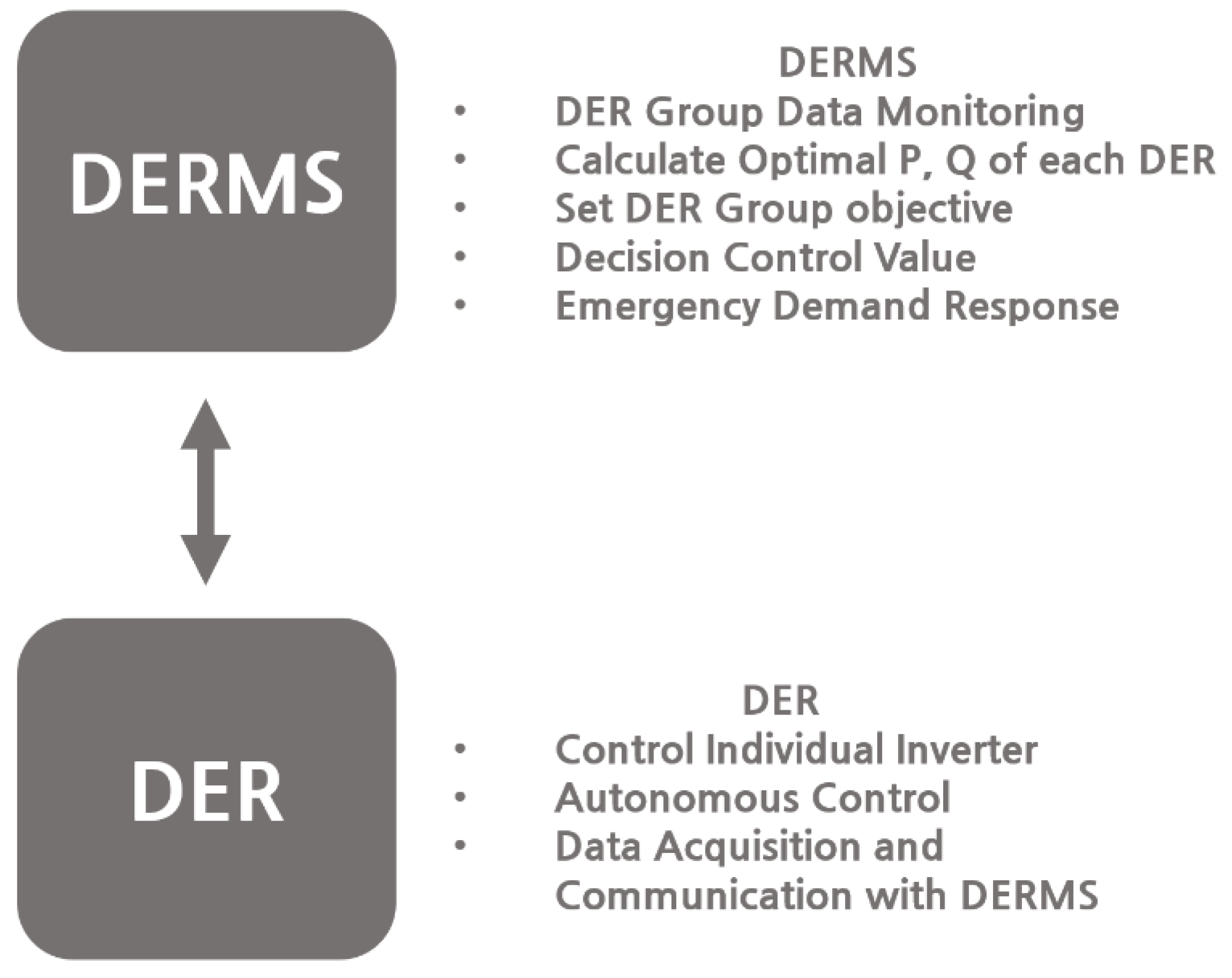
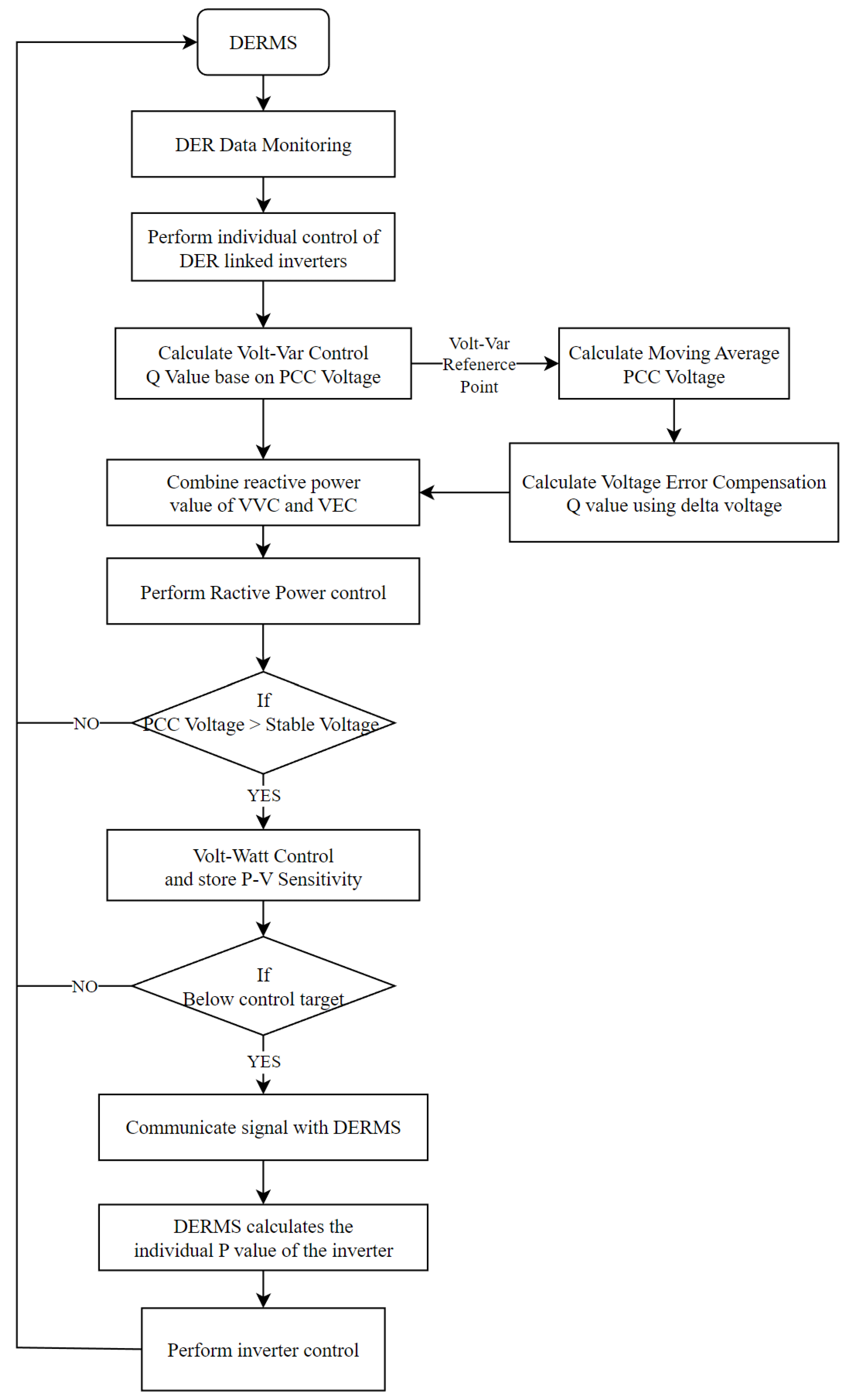
The VCS implemented by MATLAB/Simulink can be largely divided into a smart inverter model and an OpenDSS analysis engine model. In the smart inverter model, the properties of the generator are implemented and the PCC voltage is measured after the calculation is performed through communication with the OpenDSS engine. The voltage control system model is illustrated in Figure 7.
Figure 8 shows the active power and reactive power controllers of smart inverter. The smart inverter controller consists of VVC that performs reactive power control, a VEC controller, and VWC that performs active power control. PCC voltage is transmitted to each controller, and a command amount for voltage control is manifested as a controller active power value and reactive power value. The output power values of the VVC and the VEC controllers are added and then transmitted, and a saturation filter is used to design values to match the actual output power range. Thereafter, active and reactive power values are transmitted to the OpenDSS through the active power–reactive power output control curve.
There is a system linkage requirement for distributed energy resources located in the distribution line of South Korea that is used to describe the active power–reactive power output control curve. In the relationship between the active-power output rate and the reactive-power output capability, the reactive power output capability range increases from 0% to 100% as the active power output increases from 0% to 20%. Thereafter, if the active power output is maintained at 20% or more, the reactive power output maintains the 100% and the output power represents the supply and absorption capacity.
Table 2 provides a list of the MATLAB/Simulink model functions used in this work. Part A is a VCS, wherein an output control model of a smart inverter is located. Part B is an OpenDSS engine for power flow analysis and Part C is the active power output controller of the smart inverter. Part C includes the volt–watt model and the P–V sensitivity calculation model. The reactive power output is related to the active power output amount. According to the connection standard of the smart inverter distribution system the active output does not interfere with the output of the reactive output if the active output is more than 20% of the maximum output. Part D is the reactive power controller. The VVC and the VEC controller, which perform reactive power control by calculations based on the PCC voltage, are located.

5. DERMS

5.1. Concept of DERMS

A DERMS can be defined as a system that effectively manages various types of DERs installed in a power distribution system; it is a management means for grouping DERs to observe key characteristics and command control. Figure 9 shows a form of combining various devices to create a group. Connectivity is created in DERMS by the functions and features of each layer. Moreover, a DERMS serves to connect communication means between multiple distributed power sources and a central distribution management system. Through this, the distribution company can effectively manage DERs in the distribution system and individual DERs can receive instructions on effective countermeasures for various situations. Finally, a DERMS can stably pursue driving goals and economic feasibility. The hierarchical features for pursuing goals at the group level is shown in Figure 10 [21,22,23,24,25].
A flow chart illustrating the DERMS process is shown in Figure 11. The DERMS monitors the DER-linked inverter to obtain data. Each inverter performs control and communicates with DERMS if the control target is not met. The DERMS calculates the optimal value of an individual inverter and transmits it to the inverter. The inverter operates based on the commanded value.
Voltage control of the inverter linked to the DER performs voltage control autonomously in normal situations and the VCS communicates with the DER data with the DERMS. The VVC and VEC models of the inverter in the VCS perform a reactive power compensation procedure calculated based on each control curve. This procedure is performed when the PCC voltage is greater than the stable voltage range and after the reactive power value is converged. The VWC model performs active power output control and the VCS also calculates the P–V sensitivity. The P–V sensitivity is calculated from the voltage and output values before and after the VWC. If the P–V sensitivity has been calculated by this process, the higher layer can command the DER to curtailment and the DERMS commands are enforced to improve stability.

5.2. Decision of Control Values

The effect of active power control is related to the connection point. This indicates that the sensitivity of active output control is different for each smart inverter. In general, the active power output using VWC is not a method for reducing the power to a specific PCC voltage. The active power output autonomously converges to the final operating point and this point has a voltage mismatch related to the Thevenin impedance of the smart inverter.
Therefore, direct transmission of the DERMS active power operation value is the most efficient and fastest control effect. The process of calculating the operating point in the DERMS is as follows. VCS calculates the sensitivity associated with the active power of the smart inverter and the progression of the PCC voltage point and the active power output point generated by the VWC.
The P–V sensitivity is defined as follows:
S e n s i t i v i t y P , V = d V d P = V V W 0 V V W P V W 0 P V W .
The P–V sensitivity is calculated by delta active power output ( d P ) values applying voltage–watt control before and after. Moreover, the PCC voltage changes as the active power output changes ( d V ). V V W 0 in Equation (4) is the PCC voltage converged after reactive power control, V V W is the PCC voltage converged after VWC, P V W 0 is the initial active power output without active power control, and P V W is the active power output converged using the VWC.
P o r d e r = P V W 0 V V W 0 1.038 S e n s i t i v i t y P , V
Equation (4) can be organized and developed into Equation (5). As a result, P o r d e r can be calculated by applying 1.039 p.u., which is the line overvoltage standard applied in Korea.

6. Simulation Results
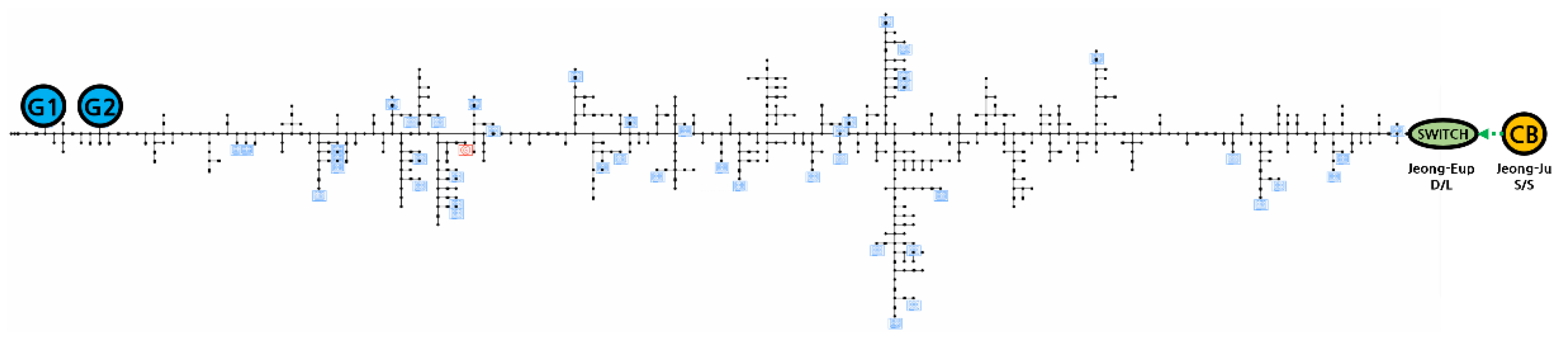
6.1. Target System

The Jeong-Eup D/L, which is the real distribution line in the Korean power system, was selected to analyze the voltage control effect of the proposed DERMS. A single-line diagram of this D/L is provided in Figure 12.
Figure 12 shows the location of the G1 and G2 smart inverters, the PV system is represented by a blue square on a single line diagram, and the fossil plant is represented by a red square.
Table 3 shows the system data for the Jeong-Eup D/L. The average capacity of the distributed generator connected at Jeong-Eup D/L is about 123 kVA. Most generators are similar in average capacity and have a wide range of DERs installed and balanced across the D/L. The DER generated output causes an overvoltage issue in the distribution network. This system data is used since it is possible to prove the voltage control effect by analyzing its impact on the overvoltage state.
Two inverters located at the end of the D/L were selected for control. The detailed specifications of the smart inverters are shown in Table 4. The capacities of inverters G1 and G2 are 1143 and 240 kVA, respectively. DERs located at the end of the D/L have a greater effect on voltage change than those located at the inlet of the feeder. The PCC voltage was analyzed by selecting inverters with the largest and next-largest capacities connected to the end of the power D/L.

6.2. Simulation Results and Discussion

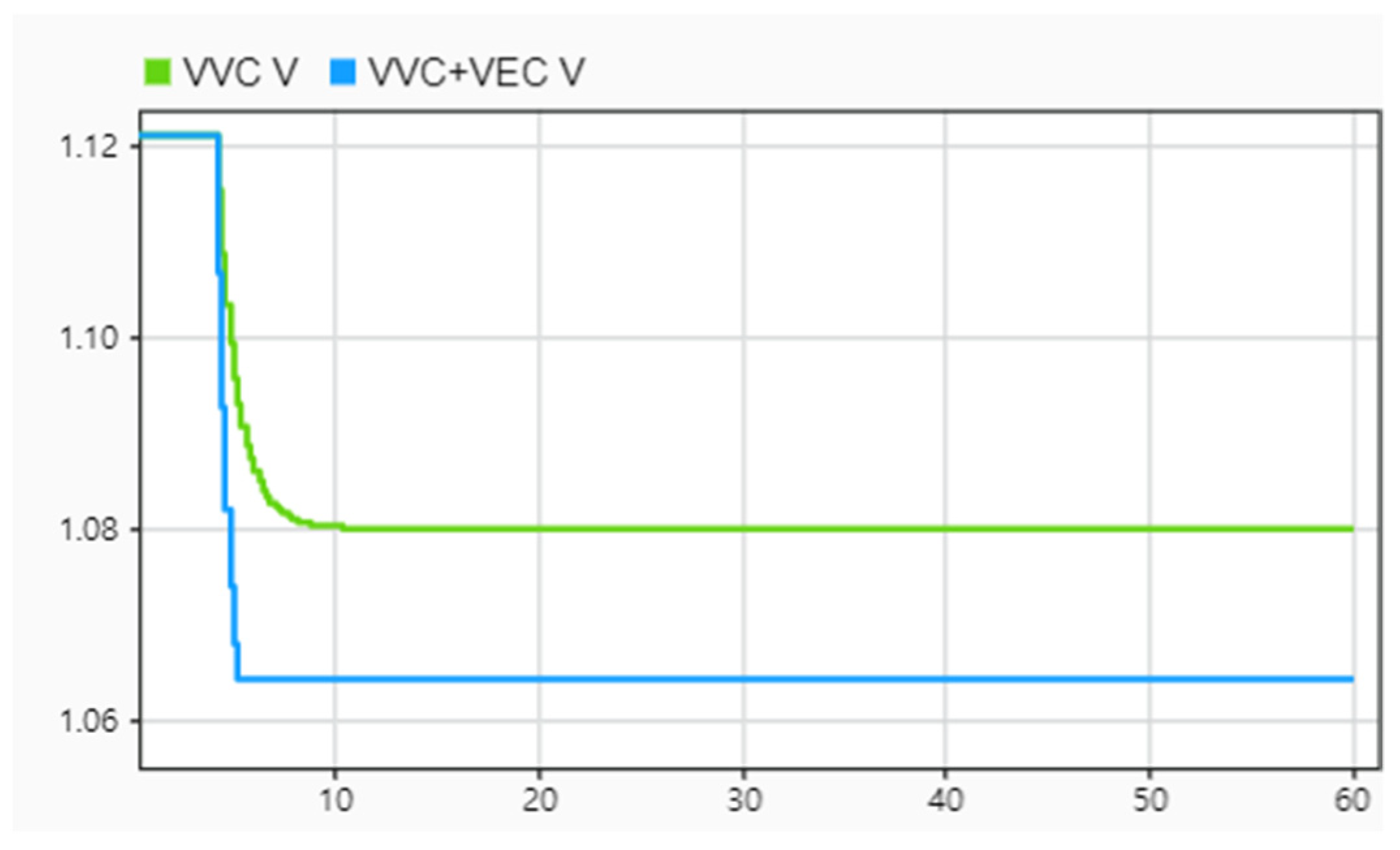
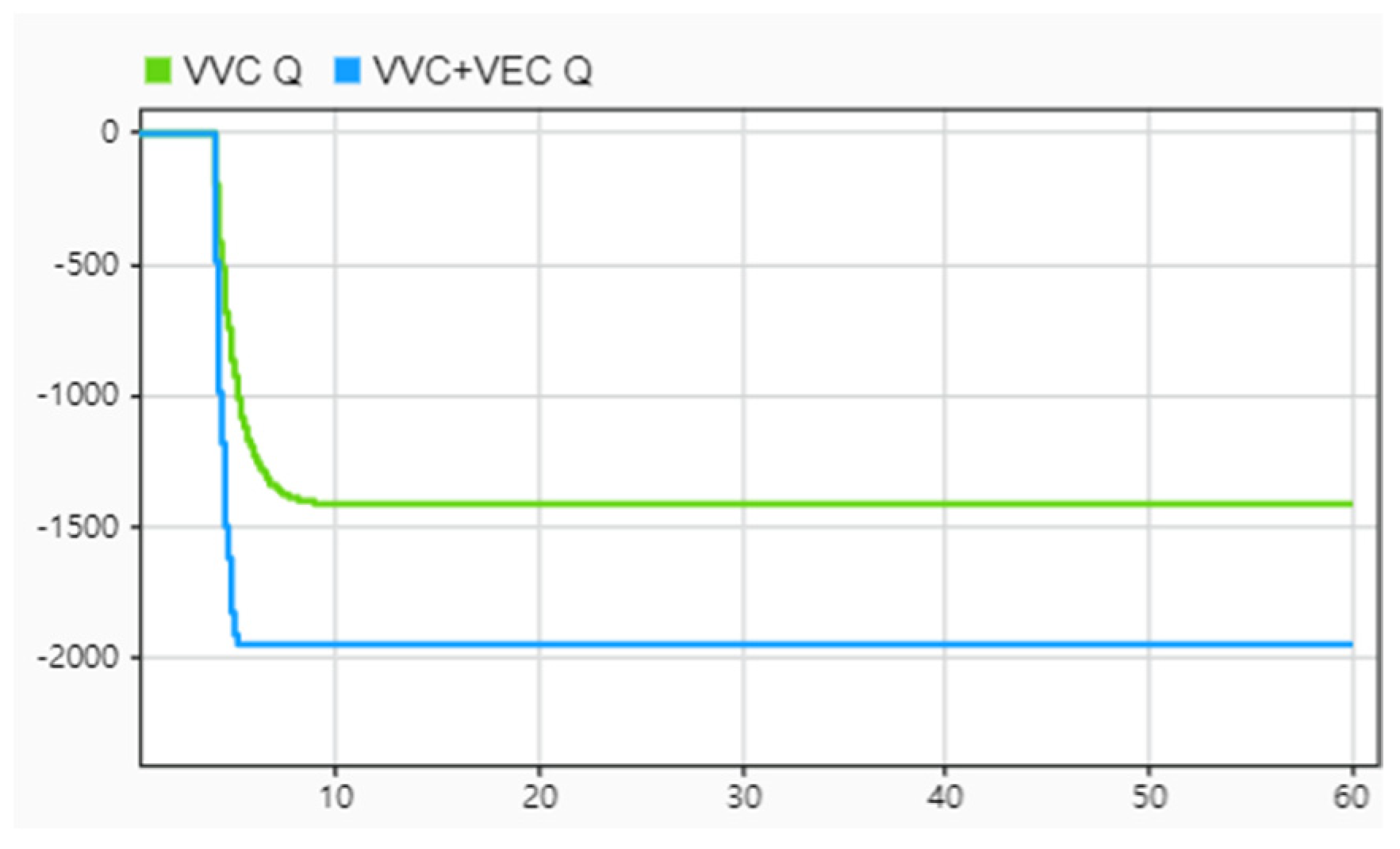
6.2.1. Comparison of VVC with VEC

To confirm the improvement of the reactive power control effect through VEC control, the following simulation was performed.
Reactive power control was performed on the G1 inverter. During this simulation, Case 1 uses only VVC control while Case 2 simultaneously uses VVC and VEC control and measures the reactive power value and PCC voltage. For effect analysis according to the control method, the controller is triggered at 4 s to perform each control and the other conditions are the same. In summary, VVC is triggered at 5 s in Case 1, and VVC and VEC are triggered simultaneously at 5 s in Case 2.
The simulation results are shown in Figure 13 and Figure 14. Figure 13 shows the PCC voltage output power of the G1 inverter and Figure 14 shows the reactive power output of the G1 inverter. In both cases, reactive power begins to be controlled in 4 s. In the case of using VEC, reactive power was absorbed up to −1937 kVar. In the case where VVC was applied, reactive power converged to −1410 kVar.
An observed difference in time and voltage finally converged, even when VVC and VEC were used together. When VVC and VEC were applied together, they converged to 1.064 p.u. at 5.4 s while VVC alone was at 1.080 p.u. at 11.7 s.
This simulation proves that voltage control is more effective when simultaneously maximizing the reactive power output with the VEC control method than when using the volt–var single control method. In the following simulations, the DERMS reactive power control algorithm is analyzed using reactive power compensation with both VVC and VEC.

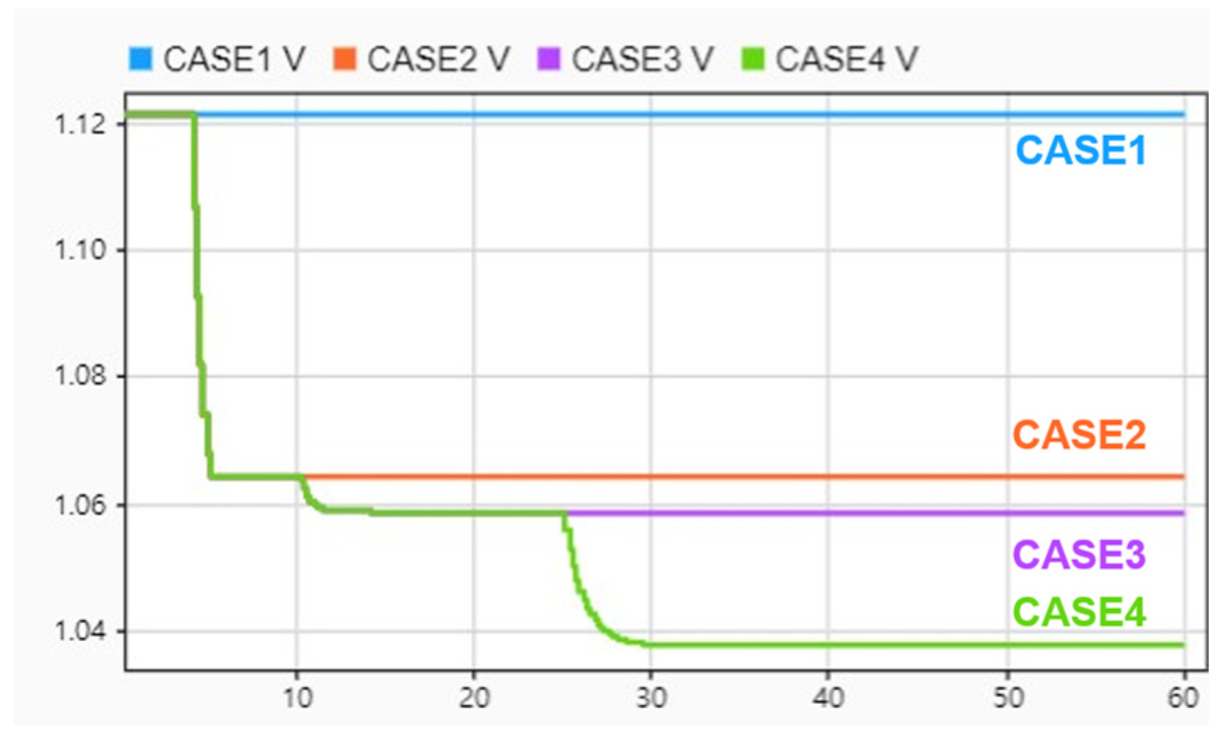
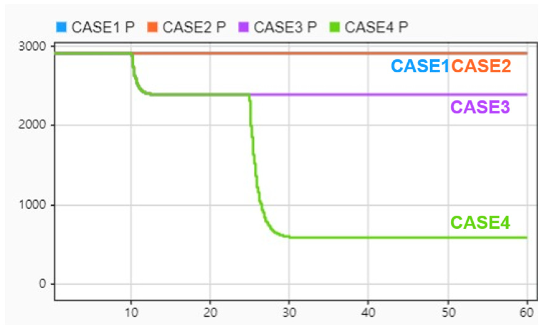
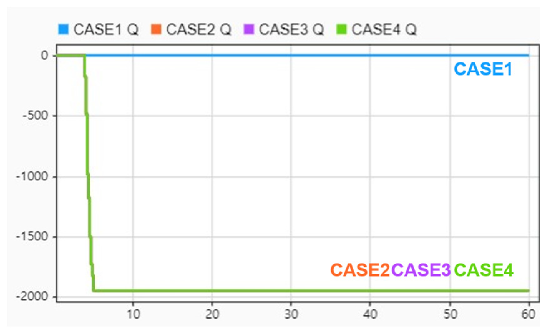
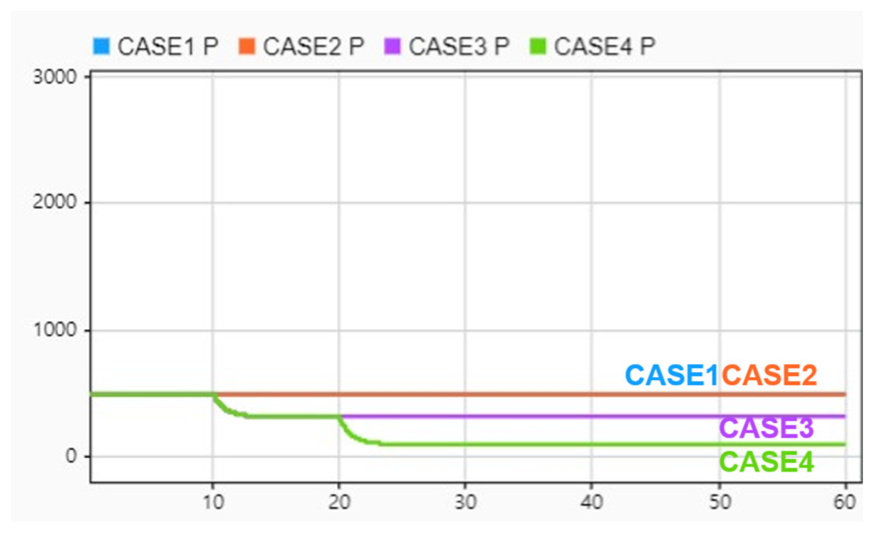
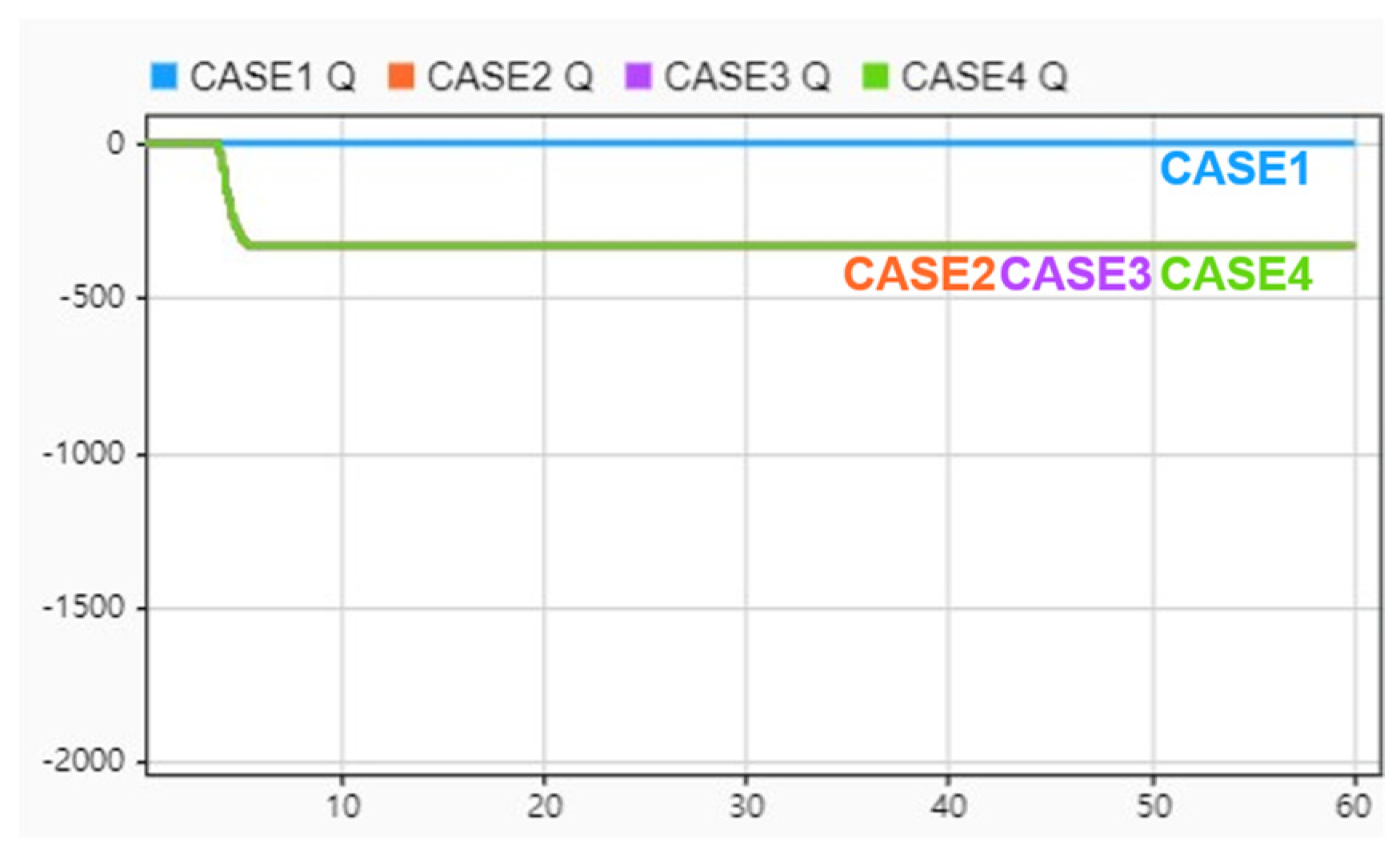
6.2.2. Verification of DERMS Effects

Four simulations were compared for each case. The PCC voltage, reactive power output, and active power output of the G1 and G2 inverters were the data used for analyzing effects. The scenarios for verifying the effectiveness of DERMS are shown in Table 5.
The VCS tracks an operating point that can stabilize the distribution network and a VCS that independently adjusts the parameters of active power and reactive power was established. The results were analyzed using the effects of power value and PCC voltage.
In Case 1, the analysis of the voltage trend, active power output, and reactive power output of the Jeong-Eup D/L was conducted. In Case 2, the effect of reactive power control was analyzed while the effect of active power control was analyzed by applying VWC in Case 3. Case 4 included the observation of voltage trends converging while controlling the active and reactive power with DERMS.
  • G1 Inverter
As shown in Figure 15, Figure 16 and Figure 17, the PCC voltage is in an overvoltage state in Case 1, which is the control generator G1 base case. In Figure 16 and Figure 17, the G2 PCC voltage converged to 1.121 p.u. (Figure 15) and the active power output was 497 kW. In the G2 inverter, Case 1 has no reactive power output. Cases 2, 3, and 4 confirmed the results according to the control in the base case.
Case 2 applies the VEC and VVC scheme in the G1 inverter, and the G1 inverter triggered the VVC and VEC at 4 s. The reactive power of G1 converged at 5.4 s. The final converged reactive power is −1937.2 kVar. The PCC voltage of G1 decreased from 1.121 to 1.065 p.u.
Case 3 applied VVC, VEC, and VWC to inverter G1. VVC and VEC were triggered at 4 s in the G1 inverter for reactive power control. The reactive power converges to −1937.2 kVar at 5.4 s, the PCC voltage at G1 decreased from 1.121 to 1.065 p.u., and the VWC was triggered at 10 s to control the overvoltage. The active power output of the G1 inverter was reduced from 2915 to 2393 kW, as shown in Figure 17. Finally, the converged PCC voltage of the G1 inverter was 1.059 p.u.
In Case 4, after applying VVC, VEC, and WWC in inverter G2, DERMS delivered voltage stabilization commands. VVC and VEC were triggered at 4 s in the G1 inverter for reactive power control. The reactive power converged from −1937.2 kVar at 5.4 s, the PCC voltage at G1 decreased from 1.121 to 1.065 p.u., and the VWC was triggered at 10 s. The active power output of the G1 inverter was limited to 2393 kW. The PCC voltage converged to 1.059 p.u. by the reactive and active power control. However, the PCC voltage was still in the high voltage range. In this situation, the DERMS issues a stabilization command at 20 s. The active power command amount was calculated to be 587 kW using the P–V sensitivity calculated during VWC control. Finally, the PCC voltage was reduced to 1.038 p.u., which is located in the stable voltage range.
  • G2 Inverter
As shown in Figure 18, Figure 19 and Figure 20, the PCC voltage is in an overvoltage state in Case 1 (control generator G2 base case). In Figure 19 and Figure 20, the G2 PCC voltage converged to 1.0795 p.u. (as shown in Figure 14). The active power output is 497 kW and, in the G2 inverter, Case 1 has no reactive power output. Cases 2, 3, and 4 confirmed the results according to the control in the base case.
The results of Case 2, which used the VEC and VVC methods in the G2 inverter, are as follows. The G2 inverter triggers the VVC and VEC at 4 s. The reactive power of G2 converged at 5.4 s. The final convergence reactive power was −329.7 kVar and, according to the absorption of reactive power, the PCC voltage of G2 decreased from 1.0795 to 1.692 p.u., thereby mitigating the PCC voltage.
Case 3 applied VVC, VEC, and VWC to inverter G2. In the G2 inverter, the VVC and VEC controllers are triggered at 4 s for the reactive power output control. The reactive power converged to −329.7 kVar at 5.4 s, the PCC voltage at G2 decreased, and the VWC was triggered at 10 s to mitigate the overvoltage. The active power output of the G2 inverter was reduced from 497 to 316.7 kW. The final convergence PCC voltage of the G2 inverter was 1.0681 p.u.
In Case 4, after applying VVC, VEC, and WWC in inverter G2, DERMS delivers voltage stabilization commands. VVC and VEC were triggered at 4 s in the G2 inverter for the reactive power control. The reactive power converged to −329.7 kVar at 5.4 s and the PCC voltage of G2 decreased to 1.0681 p.u. The VWC was triggered at 10 s to control the active power and the active power output of the inverter was reduced to 316.7 kW. Through the autonomous reactive power and active power control, the PCC voltage decreased to 1.0681 p.u. However, in this case, which controls the PCC voltage of inverter G2, the voltage is still in the high voltage range. In this situation, the DERMS issued a stabilization command at 20 s and the active value was calculated during the VWC control. Using P–V sensitivity, the active power target was limited to 99.4 kW and, at 27.6 s, the PCC voltage was finally reduced to 1.0668 p.u.
By comparing the results of control inverters G1 and G2, the final convergence PCC voltage was found to depend on the DER capacity. The active power limitation due to the DERMS command is to limit the active power output to the lowest point. However, the VCS limits the active power output to a point that does not interrupt the output of the reactive power according to the P–Q capacity curve. This power limit was 20% of the active power and the active power was reduced to the lowest point (to the actual minimum power).
In the sequence of controls, the first reactive power control is relieved by the PCC voltage and the VWC determines whether or not to trigger. If the PCC voltage is in the high voltage range, the VWC is triggered and the active power is reduced. Through this process, VCS calculates and stores the P–V sensitivity in memory. Finally, when DERMS issues a stabilization command, the active power is limited to the calculated value to maintain the PCC voltage below 1.0393 p.u. and the inverter follows the operating point.

7. Conclusions

This paper proposed a method to reduce PCC overvoltage caused by the power generation of DER in a distribution network. A control strategy for reactive and active power was developed and, consequently, control performance was improved.
The voltage control algorithm of the inverter controls the reactive power by controlling volt–var and voltage error correction. The maximum reactive power is tracked by the VEC. If the voltage can no longer be lowered using reactive power compensation, the active power control is used. The active power output control algorithm generates the active power output using a preset VWC curve after the reactive power control. If the voltage exceeds the reference voltage, the VWC curve reduces the active power output. During VWC, the VCS calculates the P–V sensitivity and stores this value. When the DERMS (the higher layer of the DER) commands control for greater stability, the VCS uses the P–V sensitivity to generate the calculated active power output and passes it to the DER. The voltage control effect was verified based on an actual distribution power system simulation of the Jeong-Eup D/L (a real distribution power system in Korea), where overvoltage was generated with the power generation of DER. MATLAB/Simulink was used to model the VCS, which was simulated with the OpenDSS power flow engine to obtain the calculation and result analysis.
The result verification analyzed the effect by stabilizing the voltage of the distribution network in an overvoltage situation. The reactive power control algorithm was used to control the reactive power to the maximum output. Active power control was applied if the overvoltage state persisted after reactive power management, and additional voltage stabilization was possible. Voltage was mitigated by controlling the active and reactive power outputs.
Finally, we demonstrated that DERMS implementation had a significant impact on voltage control. The method of controlling the inverter voltage was compared with the DER capacity. If the DER capacity is not sufficient, even if DERMS commands the DER to stabilize, the capacity cannot be reduced to a stable range since there is no room for capacity, even if it changes to voltage. The proposed control method analysis can be used to develop an inverter control method for the overvoltage problem described in this paper. In the future, an algorithm that minimizes the active power curtailment value and maintains a voltage stabilization range in DERMS will be investigated as a control target for multiple inverters.

Author Contributions

Conceptualization, D.G., Y.C. and J.S.; data curation, D.G.; formal analysis, D.G. and Y.C.; funding acquisition, Y.C.; investigation, D.G.; methodology, D.G. and Y.C.; project administration, D.G. and Y.C.; resources, D.G., Y.C. and J.S.; software, D.G.; supervision, D.G. and Y.C.; validation, D.G., Y.C. and J.S.; visualization, D.G.; writing—original draft, D.G.; writing—review and editing, D.G. and Y.C. All authors have read and agreed to the published version of the manuscript.

Funding

This research was supported by Korea Electric Power Corporation (grant number: R20XO02-18). This work was also supported by the National Research Foundation of Korea (NRF) grant funded by the Korea government (MSIT) (No. NRF-2021R1F1A1063127).

Conflicts of Interest

The authors declare no conflict of interest.

References

  1. Plan for Implementation of Renewable Energy 3020, South Korea Ministry of Trade, Industry and Energy. Implementation Proposal. 2017. Available online: https://www.motie.go.kr/motie/ne/presse/press2/bbs/bbsView.do?bbs_cd_n=81&bbs_seq_n=159996 (accessed on 17 October 2022).
  2. Republic of Korea Ministry of Trade, Industry, and Energy. 9th Basic Plan for Electricity Supply and Demand; Biennial Report; Republic of Korea Ministry of Trade, Industry, and Energy: Sejong-si, Korea, 2020.
  3. Holguin, J.P.; Rodriguez, D.C.; Ramos, G. Reverse Power Flow (RPF) Detection and Impact on Protection Coordination of Distribution Systems. IEEE Trans. Ind. Appl. 2020, 56, 2393–2401. [Google Scholar] [CrossRef]
  4. Seal, B. Standard Language Protocols for Photovoltaics and Storage Grid Integration: Developing a Common Method for Communicating with Inverter-Based Systems; Technical Update 1020906; EPRI: Palo Alto, CA, USA, 2010. [Google Scholar]
  5. IEEE Std 1547-2018 (Revision of IEEE Std 1547-2003); IEEE Standard for Interconnection and Interoperability of Distributed Energy Resources with Associated Electric Power Systems Interfaces. IEEE: Piscataway, NJ, USA, 2018. Available online: https://sagroups.ieee.org/scc21/standards/1547rev/ (accessed on 17 October 2022).
  6. Jafari, M.; Olowu, T.O.; Sarwat, A.I. Optimal Smart Inverters Volt-VAR Curve Selection with a Multi-Objective Volt-VAR Optimization using Evolutionary Algorithm Approach. In Proceedings of the 2018 North American Power Symposium (NAPS), Fargo, ND, USA, 9–11 September 2018; pp. 1–6. [Google Scholar] [CrossRef]
  7. Muthukaruppan, V.; Baran, M.E. Implementing a Decentralized Volt/VAR Scheme on a Smart Distribution System. In Proceedings of the 2020 IEEE Power & Energy Society Innovative Smart Grid Technologies Conference (ISGT), Washington, DC, USA, 17–20 February 2020; pp. 1–5. [Google Scholar] [CrossRef]
  8. Hossein, Z.S.; Khodaei, A.; Fan, W.; Hossan, S.; Zheng, H.; Fard, S.A.; Paaso, A.; Bahramirad, S. Conservation Voltage Reduction and Volt-VAR Optimization: Measurement and Verification Benchmarking. IEEE Access 2020, 8, 50755–50770. [Google Scholar] [CrossRef]
  9. Kashani, M.G.; Mobarrez, M.; Bhattacharya, S. Smart Inverter Volt-Watt Control Design in High PV-Penetrated Distribution Systems. IEEE Trans. Ind. Appl. 2019, 55, 1147–1156. [Google Scholar] [CrossRef]
  10. Parajeles, M.J.; Ramírez, R.; Valverde, G. Use of Smart Inverters for Provision of Voltage Support to Medium and High Voltage Networks. In Proceedings of the 2020 2nd Global Power, Energy and Communication Conference (GPECOM), Ephesus Izmir, Turkey, 20–23 October 2020; pp. 291–296. [Google Scholar] [CrossRef]
  11. Wang, W.; Shi, X.; Brewster, C.; Huque, A. Oscillation Mechanism and Setting Guideline for Inverter Volt-Var Control. In Proceedings of the 2020 47th IEEE Photovoltaic Specialists Conference (PVSC), New York, NY, USA, 15 June–21 August 2020; pp. 2032–2039. [Google Scholar] [CrossRef]
  12. Peppanen, J.; Deboever, J.; Coley, S.; Renjit, A. Value of derms for flexible interconnection of solar photovoltaics. In Proceedings of the CIRED 2020 Berlin Workshop (CIRED 2020), Online, 22–23 September 2020; pp. 557–560. [Google Scholar] [CrossRef]
  13. Memmel, E.; Schlüters, S.; Völker, R.; Schuldt, F.; von Maydell, K.; Agert, C. Forecast of Renewable Curtailment in Distribution Grids Considering Uncertainties. IEEE Access 2021, 9, 60828–60840. [Google Scholar] [CrossRef]
  14. Mahmoud, K.; Lehtonen, M. Comprehensive Analytical Expressions for Assessing and Maximizing Technical Benefits of Photovoltaics to Distribution Systems. IEEE Trans. Smart Grid 2021, 12, 4938–4949. [Google Scholar] [CrossRef]
  15. Liu, M.Z.; Procopiou, A.T.; Petrou, K.; Ochoa, L.F.; Langstaff, T.; Harding, J.; Theunissen, J. On the Fairness of PV Curtailment Schemes in Residential Distribution Networks. IEEE Trans. Smart Grid 2020, 11, 4502–4512. [Google Scholar] [CrossRef]
  16. Liang, Z.; Chen, H.; Wang, X.; Chen, S.; Zhang, C. Risk-Based Uncertainty Set Optimization Method for Energy Management of Hybrid AC/DC Microgrids With Uncertain Renewable Generation. IEEE Trans. Smart Grid 2019, 11, 1526–1542. [Google Scholar] [CrossRef]
  17. EPRI OpenDSS. Open Distribution System Simulator. Available online: https://sourceforge.net/projects/electricdss (accessed on 17 October 2022).
  18. KEPCO. Regulations for the Use of Electrical Equipment for Transmission and Distribution, [Attachment 4] Performance Standards for Electric Facilities for Distribution. 2020. Available online: https://cyber.kepco.co.kr/ckepco/front/jsp/CY/H/C/CYHCHP00704.jsp (accessed on 17 October 2022).
  19. Zhu, H.; Liu, H.J. Fast Local Voltage Control Under Limited Reactive Power: Optimality and Stability Analysis. IEEE Trans. Power Syst. 2015, 31, 3794–3803. [Google Scholar] [CrossRef]
  20. Gwon, D.-Y.; Choi, Y.-H.; Sim, J.-B. A Study on Voltage Control Method of Smart Inverter using Matlab-OpenDSS Co-Simulation on Distribution Networks. Trans. Korean Inst. Electr. Eng. 2022, 71, 566–573. [Google Scholar] [CrossRef]
  21. Horst, G.; Seal, B.; Gray, G. Common Functions for DER Group Management. 3002008215, EPRI Project Manager, EPRI. 2016. Available online: https://www.epri.com/research/products/3002008215 (accessed on 17 October 2022).
  22. Renjit, A. Distributed Energy Resources Management Systems. 3002014467, EPRI Project Manager, EPRI. 2018. Available online: https://www.epri.com/research/products/000000003002014467 (accessed on 17 October 2022).
  23. Renjit, A. Principles of Access for Flexible Interconnection. 3002018506, EPRI Project Manager, EPRI. 2020. Available online: https://www.epri.com/research/products/000000003002019635 (accessed on 17 October 2022).
  24. Renjit, A.; Weng, D.; HuBet, T. DERMS Reference Control Methods for DER Group Management. In Proceedings of the CIRED 2019 Conference, Madrid, Spain, 3–6 June 2019. [Google Scholar] [CrossRef]
  25. Seal, B.; Renjit, A.; Deaver, B. Understanding DERMS; Technical Update 3002013049; EPRI: Palo Alto, CA, USA, 2018. [Google Scholar]
Figure 1. Schematic illustrating the volt–var control (VVC) function. V1, V2, V3, and V4 are the boundary of the minimum PCC voltage (P1), the start of the low voltage set point (P2), the start of the high voltage set point (P3), and the boundary of the maximum PCC voltage (P4), respectively; Q1 and Q2 are the maximum capacitive and induced power generation of the inverter, respectively; the reactive power output is the dead zone where outputs of Q2 and Q3 are zero in the voltage range from V2 to V3.
Electronics 11 03661 g001
Figure 2. Stable VVC operation.
Electronics 11 03661 g002
Figure 3. Unstable VVC operation (oscillation).
Electronics 11 03661 g003
Figure 4. Illustration of a volt–watt control curve.
Electronics 11 03661 g004
Figure 5. Illustration of the moving-average calculation.
Electronics 11 03661 g005
Figure 6. Illustration of the voltage error compensation curve.
Electronics 11 03661 g006
Figure 7. Illustration of the voltage control system model in MATLAB/Simulink.
Electronics 11 03661 g007
Figure 8. Illustration of the smart inverter active power and reactive power controllers.
Electronics 11 03661 g008
Figure 9. Connectivity of DERMS.
Electronics 11 03661 g009
Figure 10. Hierarchical features of DERMS.
Electronics 11 03661 g010
Figure 11. Flow chart illustrating the DERMS process.
Electronics 11 03661 g011
Figure 12. Single-line diagram of the Jeong-Eup D/L. G1 and G2 indicate the smart inverters while PV systems are represented by blue squares and the fossil plant is represented by a red square.
Electronics 11 03661 g012
Figure 13. PCC voltage of the G1 inverter.
Electronics 11 03661 g013
Figure 14. Reactive power output of G1 Inverter.
Electronics 11 03661 g014
Figure 15. PCC voltage of the G1 inverter.
Electronics 11 03661 g015
Figure 16. Active power output of the G1 Inverter.
Electronics 11 03661 g016
Figure 17. Reactive power output of the G1 Inverter.
Electronics 11 03661 g017
Figure 18. PCC voltage of the G2 inverter.
Electronics 11 03661 g018
Figure 19. Active power output of the G2 inverter.
Electronics 11 03661 g019
Figure 20. Reactive power output of the G2 inverter.
Electronics 11 03661 g020
Table 1. VEC curve parameter settings.
ParameterVoltage (p.u.)ParameterReactive Power
V 1 −0.06 Q 1 Q m a x
V 2 −0.01 Q 2 0
V 3 0.01 Q 3 0
V 4 0.06 Q 4 Q m i n
Table 2. MATLAB/Simulink model functions.
PartsFunction
AVoltage Control System
BOpenDSS engine
CActive Power Output Controller
DReactive Power Output Controller
Table 3. System data of the Jeong-Eup D/L distribution networks.
Distributed
Energy Resources
Distributed
Generation Capacity
Loads
4713,832 kVA1199 kVA
Table 4. Detailed specifications for the smart inverters.
InverterDER CapacityActive Power
Maximum Output
Reactive Power
Output Range
G13500 kVA2915 kW±1937 kVar
G2596.4 kVA497 kW±329.6 kVar
Table 5. Simulation scenarios.
CaseScenarios
1Base Case (No Control)
2VEC
3VEC and VWC
4VEC and VWC with DERMS
Publisher’s Note: MDPI stays neutral with regard to jurisdictional claims in published maps and institutional affiliations.

